 | –≠–ª–µ–∫—Ç—Ä–æ–Ω–Ω—ã–π –∫–æ–º–ø–æ–Ω–µ–Ω—Ç: LC75010W | –°–∫–∞—á–∞—Ç—å:  PDF PDF  ZIP ZIP |
Ordering number : ENN7349
N2103TN (OT) No. 7349-1/12
Overview
The LC75010W is a car audio DSP IC that integrates the
signal processing required by car audio systems, A/D and
D/A converters, volume control, and other functions on a
single chip. It can implement a car audio system with a
minimal number of external components.
Features
∑ Hardware Functions
-- Analog source selector (BTL:1ch, OTL:3 ch)
-- 20 bits A/D (2ch)
-- 24 bits DSP (core, program memory, data memory)
-- SIO (CCB I/F) (CCB is LSB first input.)
-- 24 bits D/A (4ch)
-- EVR (4ch)
∑ Software Functions* (See Note.)
-- Bass/Mid/Treb
-- Bal/Fad
-- Fixed equalizer (Front/Rear/separately controlled)
-- Loudness control
-- Hybrid volume
-- Anti-hard clip
-- Dedekind (Speaton**)
Note *: Software specifications can be modified in
response to user requests.
∑ DSP Functions (24 fixed-point DSP)
-- Program ROM -- 8k words
-- Data RAM -- 896 words
∑ Supply Voltage and Package Specifications
-- DSP core, A/D converter (digital block), D/A
converter (digital block): 3.3 V
-- A/D converter (analog block), D/A converter
(analog block), volume control, crystal oscillator:
5 V
-- Package: 100-pin SQFP (14
◊
14 mm)
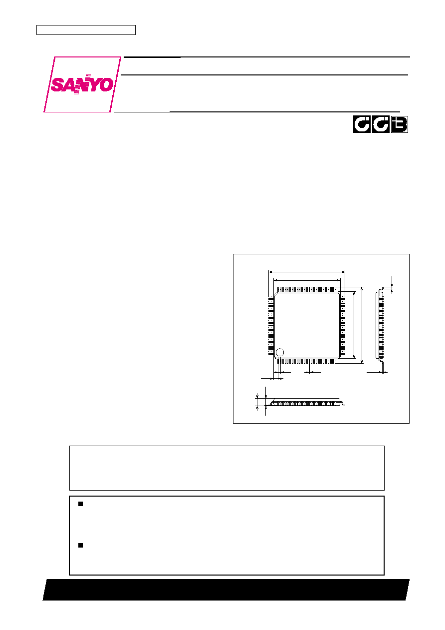
Package Dimensions
unit: mm
3181C-SQFP100
14.0
16.0
14.0
16.0
0.145
0.2
0.5
(1.0)
(1.4)
1.6max
0.1
0.5
1
25
26
50
51
75
76
100
SANYO: SQFP100
[LC75010W]
LC75010W
SANYO Electric Co.,Ltd. Semiconductor Company
TOKYO OFFICE Tokyo Bldg., 1-10, 1 Chome, Ueno, Taito-ku, TOKYO, 110-8534 JAPAN
LC75010W Car Audio DSP
CMOS IC
Any and all SANYO products described or contained herein do not have specifications that can handle
applications that require extremely high levels of reliability, such as life-support systems, aircraft's
control systems, or other applications whose failure can be reasonably expected to result in serious
physical and/or material damage. Consult with your SANYO representative nearest you before using
any SANYO products described or contained herein in such applications.
SANYO assumes no responsibility for equipment failures that result from using products at values that
exceed, even momentarily, rated values (such as maximum ratings, operating condition ranges, or other
parameters) listed in products specifications of any and all SANYO products described or contained
herein.
∑ CCB is a registered trademark of Sanyo Electric Co., Ltd.
∑ CCB is Sanyo's original bus format. All bus addresses are managed by Sanyo for this format.
Note
**
: Speaton is a registered trademark of Dedekind R&D. Users who want to develop, manufacture,
or sell electronic equipment that uses Dedekind functions must enter a separate contract with
Dedekind R&D for the use of those functions.

No. N7349-2/12
LC75010W
Parameter
Symbol
Pin name
Ratings
Unit
min
typ
max
Supply voltage
V
DDmax1
AV
DD1
, AV
DD2
, AV
DD5
, AV
DD6
, AV
DD7
, AV
DD8
, AV
DD9
,
≠0.3
+6.0
V
(A/D, D/A, volume, etc)
AV
DD10
, AV
DD11
, AV
DD12
Supply voltage (crystal oscillator)
V
DDmax2
XV
DD
≠0.3
+6.0
V
Supply voltage
V
DDmax3
DV
DD1
, DV
DD2
, DV
DD3
, DV
DD4
, DV
DD5
, DV
DD6
, AV
DD4
≠0.3
+4.0
V
(DSP core block)(I/O I/F, PLL block)
Maximum input voltage
AINRP1, AINRN1, AINLP1, AINLN1, AINRP2,AINLP2,
V
DDmax1
(A/D, D/A, volume, etc)
V
IN
1
AINRP3, AINLP3, AINRP4, AINLP4,
≠0.3
+ 0.3
V
VFLI, VFRI, VRLI, VRRI
(max +6.0 V)
Maximum input voltage
TEST0, TEST1, TEST2, TEST3, TEST4, TEST5,
V
DDmax3
(DSP core block)
V
IN
2
TEST6, TEST7, TEST8, TEST9, TEST10,
≠0.3
+ 0.3
V
(I/O I/F block)
TEST13, TEST14, PWDB
(max +4.0 V)
V
IN
3
CL, CE, DI, RSTB, INTB
≠0.3
+6.0
V
Allowable power dissipation
Pdmax
(Conditions: Audio disabled operating state, Std. Board
installation ; See note)
830
mW
Maximum output current
Io
DO
0
6.0
mA
Operating temperature
Topr
≠40
85
∞C
Storage temperature
Tstg
≠55
125
∞C
Parameter
Symbol
Pin name
Ratings
Unit
min
typ
max
Supply voltage
AV
DD5
AV
DD1
, AV
DD2
, AV
DD5
, AV
DD6
, AV
DD7
, AV
DD8
, AV
DD9
,
+4.75
+5.25
V
(analog block)
AV
DD10
, AV
DD11
, AV
DD12
Supply voltage (crystal oscillator)
XV
DD5
XV
DD
+4.75
+5.25
V
Supply voltage
DV
DD3.3
DV
DD1
, DV
DD2
, DV
DD3
, DV
DD4
, DV
DD5
, DV
DD6
, AV
DD4
+3.0
+3.6
V
(digital block, PLL)
PWDB, INITB, TEST0, TEST1, TEST2, TEST3, TEST4,
High-level input voltage
V
IHD
TEST5, TEST6, TEST7, TEST8, TEST9, TEST10,
0.7
◊
DV
DD3.3
DV
DD3.3
V
TEST13, TEST14
V
IHD1
CL, CE, DI, RSTB
0.7
◊
AV
DD5
AV
DD5
V
PWDB, INITB, TEST0, TEST1, TEST2, TEST3, TEST4,
Low-level input voltage
V
ILD
TEST5, TEST6, TEST7, TEST8, TEST9, TEST10,
V
SS
0.3
◊
DV
DD3.3
V
TEST13, TEST14
V
ILD1
CL, CE, DI, RSTB
V
SS
0.3
◊
AV
DD5
V
AINRP1, AINRN1, AINLP1, AINLN1, AINRP2,
Full-scale input level
AINLP2, AINRP3, AINLP3, AINRP4, AINLP4
0.4
◊
AV
DD5
Vp-p
Crystal oscillator frequency
*
X
IN
, X
OUT
16.9344
MHz
Allowable Operating Ranges
at Ta = ≠40 to +85∞C, V
SS
D = V
SS
A = 0 V
Specifications
Absolute Maximum Ratings
at Ta = 25∞C, V
SS
= 0 V
Note Std. board : 114.3 mm
◊
76.2 mm
◊
1.5 mm, material ; glass epoxy resin
Note
*
: Consult with the manufacturer of the crystal oscillator element used to verify that the circuit constant values are appropriate for that crystal
oscillator element before using this circuit.

No. N7349-3/12
LC75010W
Electrical Characteristics in the Allowable Operating Ranges
Parameter
Symbol
Pin name
Ratings
Unit
min
typ
max
PWDB, RSTB, INTB, CE, CL, DI, TEST0,
High-level input current
I
IH
TEST1, TEST2, TEST3, TEST4, TEST5, TEST6,
5
µA
TEST7, TEST8, TEST9, TEST10, TEST13, TEST14
PWDB, RSTB, INTB, CE, CL, DI, TEST0,
Low-level input current
I
IL
TEST1, TEST2, TEST3, TEST4, TEST5, TEST6,
≠5
µA
TEST7, TEST8, TEST9, TEST10, TEST13, TEST14
BUSY, DO, TEST11, TEST12 (Microcontroller: 5 V)
4.5
5.5
V
High-level output voltage
V
OH
BUSY, DO, TEST11, TEST12 (Microcontroller: 3.3 V)
3.0
3.6
V
Low-level output voltage
V
OL
BUSY, DO, TEST11, TEST12
0.5
V
Analog output level
V
OUT
A
OUT1
, A
OUT2
, A
OUT3
, A
OUT4
0.6
◊
AV
DD5
V
P-P
Vref1
Reference voltage output
Vref2
Vref1, Vref2, Vref3
2.35
2.5
2.65
V
Vref3
(Conditions: Audio disabled operating state, Std. board
I
AVDD5
installed ; See note)
55
72
mA
A
VDD5
= X
VDD5
= 5V, D
VDD3.3
= 3.3 V
(Conditions: Audio disabled operating state, Std. board
I
XVDD5
installed ; See note)
5
7
mA
Current drain
A
VDD5
= X
VDD5
= 5V, D
VDD3.3
= 3.3 V
(Conditions: Audio disabled operating state, Std. board
I
DVDD3.3
installed ; See note)
65
85
mA
A
VDD5
= X
VDD5
= 5V, D
VDD3.3
= 3.3 V
(Conditions: Audio disabled operating state, Std. board
Pd
installed ; See note)
515
680
mW
Power dissipation
A
VDD5
= X
VDD5
= 5V, D
VDD3.3
= 3.3 V
Parameter
Conditions
Ratings
Unit
min
typ
max
S/N
A-weighted, Input conditions: 2 Vp-p
85
90
--
dB
Dynamic range
A-weighted
85
90
--
dB
THD+N
Input conditions: 1.5 Vp-p. See note.
--
≠86
≠80
dB
Conditions: Analog system: 5 V, digital system: 3.3 V, fs: 44.1 kHz, signal frequency: 1 kHz, from the analog source selector input to the
volume control circuit output.
Measurement band: 10 Hz to 20 kHz, using the SANYO-specified DSP evaluation board.
Test circuit: LC75010W external circuit structure with the DSP operating in through mode (4-bit shiftup), room temperature
Test equipment: Audio analyzer (Rohde & Schwarz UPD)
LC75010W Analog Characteristics
Note: THD+N shows the optimal characteristics for an input (1.5 Vp-p) that is 3 dB lower than the full-scale input level.
Parameter
Symbol
Pin name
Ratings
Unit
min
typ
max
Data setup time
t
SU
DI, CL
0.75
µs
Data hold time
t
HD
DI, CL
0.75
µs
Clock low-level time
t
CL
CL
0.75
µs
Clock high-level time
t
CH
CL
0.75
µs
CE wait time
t
EL
CE, CL
0.75
µs
CE setup time
t
ES
CE, CL
0.75
µs
CE hold time
t
EH
CE, CL
0.75
µs
Data latch change time
t
LC
0.75
µs
Data output time
t
DC
DO, CL
0.35
µs
t
DH
DO, CE
CCB Timing
Note Std. board : 114.3 mm
◊
76.2 mm
◊
1.5 mm, material : glass epoxy resin

No. N7349-4/12
LC75010W
Pin Assignments
AVDD8
VFLO
VFLI
AOUT1
VFRO
VFRI
AOUT2
AVSS7
AVDD7
Vref2
AVB2
NC
NC
AVSS6
AVDD6
AOUT3
VRLI
VRLO
AOUT4
VRRI
VRRO
AVSS5
AVDD5
XVDD
XVSS
AVSS0
AVSS1
AVDD1
AVDD2
AVSS2
AVSS3
AVB1
DVSS1
DVDD1
TEST0
TEST1
TEST2
TEST3
TEST4
DVSS2
DVDD2
TEST5
TEST6
TEST7
TEST8
TEST9
TEST10
DVB1
DVSS3
DVDD3
AVDD4
VCO
PDO
AVSS4
DVDD4
DVSS4
DVB2
BUSY
PWDB
RSTB
CE
CL
DI
DO
INTB
TEST11
DVSS5
DVDD5
TEST12
TEST13
TEST14
DVSS6
DVDD6
XIN
XOUT
Vref1
AVSS12
AVDD12
AINRP1
Ars4
Ars3
AINRN1
AINRP4
AINRP3
AVSS11
AVDD11
AINRP2
AVDD9
AVSS9
Vref3
AINLP2
AVDD10
AVSS10
AINLP3
AINLP4
AINLN1
Als3
Als4
AINLP1
AVSS8
26
27
28
29
30
31
32
33
34
35
36
37
38
39
40
41
42
43
44
45
46
47
48
49
50
75
74
73
72
71
70
69
68
67
66
65
64
63
62
61
60
59
58
57
56
55
54
53
52
51
100
99
98
97
96
95
94
93
92
91
90
89
88
87
86
85
84
83
82
81
80
79
78
77
76
1
2
3
4
5
6
7
8
9
10
11
12
13
14
15
16
17
18
19
20
21
22
23
24
25
LC75010W
(Top view)

No. N7349-5/12
LC75010W
Pin Functions
Pin No.
Pin name
Input/Output (I/O)
Function
97
AINRP1
I
Analog BTL input (Rch +)
94
AINRN1
I
Analog BTL input (Rch -)
77
AINLP1
I
Analog BTL input (Lch +)
80
AINLN1
I
Analog BTL input (Lch -)
89
AINRP2
I
Analog OTL input1 (Rch +)
85
AINLP2
I
Analog OTL input1 (Lch +)
92
AINRP3
I
Analog OTL input2 (Rch +)
82
AINLP3
I
Analog OTL input2 (Lch +)
93
AINRP4
I
Analog OTL input3 (Rch +)
81
AINLP4
I
Analog OTL input3 (Lch +)
Standby mode (active low)
Setting the PWDB pin to the low level sets the LC75010W to standby mode (also know as "power
down mode").
34
PWDB
I
In standby mode, the DSP system clock and the crystal oscillator are stopped and the whole
LC75010W goes to the stopped state. This pin must be held at the high level during normal
operation.
Reset (active low)
35
RSTB
I
A reset is normally applied at power on, after recovering from a temporary power outage, and after
returning from standby mode ("power down mode").
Interrupt (active low) (Software clip input (0/1))
40
INTB
I
Provides feedback control to the DSP to prevent clipping when an overflow occurs in the amplifier
output.
10
TEST0
I/O
Test pin
11
TEST1
I/O
Test pin
12
TEST2
I/O
Test pin
13
TEST3
I/O
Test pin
14
TEST4
I/O
Test pin
17
TEST5
I/O
Test pin
18
TEST6
I/O
Test pin
19
TEST7
I/O
Test pin
20
TEST8
I/O
Test pin
21
TEST9
I/O
Test pin
22
TEST10
I/O
Test pin
41
TEST11
I/O
Test pin
44
TEST12
I/O
Test pin
45
TEST13
I/O
Test pin
46
TEST14
I/O
Test pin
49
XIN
I
Crystal input (384 fs = 16.9344 MHz) (fs = 44.1 kHz)
50
XOUT
O
Crystal output
27
VCO
I
VCO control
28
PDO
O
Charge pump output
36
CE
I
CCB enable
37
CL
I
CCB clock
38
DI
I
Data in
39
DO
O
Data out
CCB ready monitor
33
BUSY
O
Outputs the state of the DSP CCB receive buffer.
A low-level output from the BUSY pin indicates that the buffer is empty.
A high-level output indicates that command data is present in the receive buffer.
74
VFLO
O
Volume front Lch output
73
VFLI
I
Volume front Lch input
71
VFRO
O
Volume front Rch output
70
VFRI
I
Volume front Rch input
58
VRLO
O
Volume rear Lch output
59
VRLI
I
Volume rear Lch input
55
VRRO
O
Volume rear Rch output
56
VRRI
I
Volume rear Rch input
Continued on next page.