 | –≠–ª–µ–∫—Ç—Ä–æ–Ω–Ω—ã–π –∫–æ–º–ø–æ–Ω–µ–Ω—Ç: LC75281 | –°–∫–∞—á–∞—Ç—å:  PDF PDF  ZIP ZIP |

Ordering number : EN5913
101698RM (OT) No. 5913-1/10
Overview
The LC75281E is a four-band stereo parametric equalizer.
A parametric equalizer is a fully general equalizer that
allows all three parameters that define an equalizer's
characteristics, i.e., the center frequency, gain, and Q, to
be set independently.
Functions
∑ Four-band (low, low mid, high mid, and high) left and
right channels parametric equalizer
∑ For each band:
Center frequency: 11 positions
Gain: 13 positions in ±2dB steps
Q: Variable over 8 positions
∑ The center frequency, gain, and Q control settings are
set using serial data input in the CCB format.
Features
∑ A parametric equalizer with the following features can
be implemented with just two ICs: this IC and a
microcontroller.
∑ The center frequency, gain, and Q can be controlled by a
single operation.
∑ Memory recall by a single operation can be implement-
ed using preset values.
∑ Either shelving or peaking characteristics can be
selected for the low band.
Package Dimensions
unit: mm
3159-QFP64E
LC75281E
SANYO Electric Co.,Ltd. Semiconductor Bussiness Headquarters
TOKYO OFFICE Tokyo Bldg., 1-10, 1 Chome, Ueno, Taito-ku, TOKYO, 110-8534 JAPAN
Parametric Equalizer System
CMOS IC
Any and all SANYO products described or contained herein do not have specifications that can handle
applications that require extremely high levels of reliability, such as life-support systems, aircraft's
control systems, or other applications whose failure can be reasonably expected to result in serious
physical and/or material damage. Consult with your SANYO representative nearest you before using
any SANYO products described or contained herein in such applications.
SANYO assumes no responsibility for equipment failures that result from using products at values that
exceed, even momentarily, rated values (such as maximum ratings, operating condition ranges, or other
parameters) listed in products specifications of any and all SANYO products described or contained
herein.
SANYO: QFP64E (QIP64E)
[LC75281E]
∑ CCB is a trademark of SANYO ELECTRIC CO., LTD.
∑ CCB is SANYO's original bus format and all the bus
addresses are controlled by SANYO.
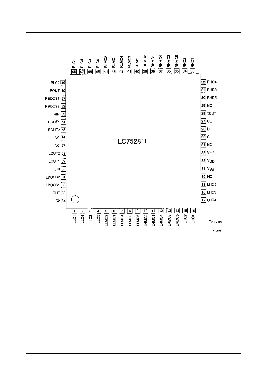
Pin Assignment
No. 5913-2/10
LC75281E

Specifications
Absolute Maximum Ratings
at Ta = 25∞C, V
SS
= 0 V
Allowable Operating Ranges
at Ta = ≠40 to +85∞C, V
SS
= 0 V
Electrical Characteristics
at Ta = 25∞C, f = 1 kHz, V
DD
= 8 V, V
SS
= 0 V
Pin Functions
No. 5913-3/10
LC75281E
Parameter
Symbol
Conditions
Ratings
Unit
Maximum supply voltage
V
DD
max
10.5
V
Maximum input voltage
V
IN
1 max
LIN, RIN
0 to V
DD
V
V
IN
2 max
CL, CE, DI
0 to V
DD
V
Allowable power dissipation
Pd max
Ta
85∞C
300
mW
Operating temperature
Topr
≠40 to +85
∞C
Storage temperature
Tstg
≠50 to +125
∞C
Parameter
Symbol
Conditions
Ratings
Unit
min
typ
max
Supply voltage
V
DD
6.0
9.0
V
High-level input voltage
V
IH
CL, CE, DI
4.0
V
DD
V
Low-level input voltage
V
IL
CL, CE, DI
V
SS
1.0
V
Input voltage range
V
IN
LIN, RIN
0
V
DD
V
Load resistance
R
L
LOUT, ROUT, MIXOUT
1
k
Input pulse width
t¯w
CL
1
µs
Setup time
tsetup
CL, CE, DI
1
µs
Hold time
thold
CL, CE, DI
1
µs
Operating frequency
fopg
CL
500
kHz
Parameter
Symbol
Conditions
Ratings
Unit
min
typ
max
Current drain
I
DD
V
DD
36
50
mA
Output voltage
V
O
LOUT, ROUT: THD = 1%
2.2
Vrms
THD1
LOUT, ROUT: Vo = Flat, V
IN
= 0 dBV
0.005
0.01
%
Total harmonic distortion
THD2
LOUT, ROUT: Vo = Boost,
0.1
1
%
All bands +2 dB, V
IN
= ≠15 dBV
V
N
1
LOUT, ROUT: Vo = Flat,
7
15
µs
Rg = 1 k
, IHF-A filters
V
N
2
LOUT, ROUT: Vo = Flat,
13
µs
Rg = 1 k
, DIN filters
LOUT, ROUT, Rg = 1 k
, f0 = f1, Q = Q1
Output noise voltage
V
N
3
IHF-A filter, all bands at full boost, with the external
58
µs
constants the same as those for the center
frequency (example 1)
LOUT, ROUT, Rg = 1 k
, f0 = f1, Q = Q1
V
N
4
IHF-A filters, all bands at full cut, with the external
23
µs
constants the same as those for the center frequency
(example 1)
Crosstalk between inputs
CT
V
IN
= 1 Vrms, f = 1 kHz
60
80
dB
High-level input current
I
IH
CL, DI, CE, V
IN
= 9 V
1
µA
Low-level input current
I
IL
CL, DI, CE, V
IN
= 0 V
≠1
µA
All bands
DC variation
V
DC
G = +12 dB, Q: Setting switched from Q1 to Q2
≠10
+10
mV
With the external constants the same as those for the
center frequency (example 1) shown on page 7.
Pin No.
Pin
Function
64
LLC2
1
LLC1
2
LLC4
3
LLC3
4
LLC5
5
LLMC2
6
LLMC1
7
LLMC4
8
LLMC3
Left channel low band control block.
External capacitor connections.
Left channel low mid band control block.
External capacitor connections.
Continued on next page.

Continued from preceding page.
No. 5913-4/10
LC75281E
Pin No.
Pin
Function
10
LHMC2
11
LHMC1
12
LHMC4
13
LHMC3
14
LHMC5
15
LHC2
16
LHC1
17
LHC4
18
LHC3
19
LHC5
20, 24, 29
NC
Unused pins. These pins must be either left open or connected to V
SS
.
56, 57
23
Vref
Internal operational amplifier reference voltage generator outputs.
Several capacitors with values of about 10 µF must be connected with this pin to reduce ripple.
21
V
SS
Power supply.
22
V
DD
These pins must be connected to the stipulated power supply.
27
CE
26
DI
Serial data and clock inputs for IC control
25
CL
49
RLC2
48
RLC1
47
RLC4
46
RLC3
45
RLC5
44
RLMC2
43
RLMC1
42
RLMC4
41
RLMC3
40
RLMC5
39
RHMC2
38
RHMC1
37
RHMC4
36
RHMC3
35
RHMC5
34
RHC2
33
RHC1
32
RHC4
31
RHC3
30
RHC5
58
LCUT2
59
LCUT1
61
LBOOS2
62
LBOOS1
55
RCUT2
54
RCUT1
52
RBOOS2
51
RBOOS1
60
LIN
Left channel audio signal input (Must be driven with a low load capacitance.)
53
RIN
Right channel audio signal input (Must be driven with a low load capacitance.)
63
LOUT
Left channel audio signal output (Must be received with a low load capacitance.)
50
ROUT
Right channel audio signal output (Must be received with a low load capacitance.)
28
TEST
IC test pin.
This pin must be left open when not used for IC test.
Left channel high mid band control block.
External capacitor connections.
Left channel high band control block.
External capacitor connections.
Chip enable input. Data is written to the internal latch and the analog switches operate when this pin
changes from high to low. Data transfer is enabled when this pin is high.
Right channel low band control block.
External capacitor connections.
Right channel low mid band control block.
External capacitor connections.
Right channel high mid band control block.
External capacitor connections.
Right channel high band control block.
External capacitor connections.
Internal filter DC offset voltage exclusion capacitor connections.
Capacitors of about 10 µF must be connected between pins 61 and 62, and between pins 63 and 64.
(These are for the left channel block.)
Internal filter DC offset voltage exclusion capacitor connections.
Capacitors of about 10 µF must be connected between pins 51 and 52, and between pins 49 and 50.
(These are for the right channel block.)

Block Diagram
No. 5913-5/10
LC75281E
Low band
Low mid band
High mid band
High band
The blocks enclosed in dotted
lines are identical.