Ordering number : ENN6867
20901RM (OT) No. 6867-1/28
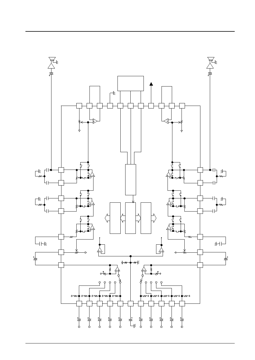
Overview
The LC75343M is an electronic volume system that can
control the volume, balance, 2-band equalizer, super bass,
and input switching functions by serial data input.
Functions
∑ Volume: 0 dB to ≠78 dB (1-dB step) and ≠
(64
positions)
0 dB to ≠50 dB (1-dB step), ≠50 dB to ≠70 dB
(2-dB step), ≠70-dB to ≠78 dB (4-dB step)
Balance function with separate L/R control
∑ Treble: ±10-dB control in 2-dB steps is possible.
Shelving characteristic.
∑ Bass*: ±10-dB control in 2-dB steps is possible. Peaking
characteristics.
∑ Super bass*: +10-dB control in 2-dB steps is possible.
Peaking characteristics.
(+/≠10 dB control in 2-dB steps is possible
depending on software support and the
application. Peaking characteristics.)
∑ Selector: 5 input signals can be selected both for
L and R
∑ Input gain: 0 dB to +30 dB (2-dB step) amplification is
possible for the input signal.
∑ General-purpose amp (ATT): 2 on-chip general-purpose
amplifiers
(0-dB to ≠18-dB in 2-dB
steps and ≠
11 positions
attenuate control is
possible, depending on
software support and the
application)
Note*: Regarding (Bass) and (Super bass) above, MID
and BASS functions can also be realized by
changing the capacitor capacitance.
Features
∑ On-chip buffer amplifier cuts down number of external
components
∑ Low switching noise generated by on-chip switch due to
use of silicon gate CMOS process
∑ On-chip reference voltage circuit for analog ground
∑ Controls performed with serial data input (CCB)
Package Dimensions
unit: mm
3263-MFP36SDJ (375 mil)
1
18
36
19
0.8
15.2
0.3
0.65
10.5
7.9
0.25
(0.8)
2.45max
0.1
(2.25)
SANYO: MFP36SDJ (375 mil)
[LC75343M]
LC75343M
SANYO Electric Co.,Ltd. Semiconductor Company
TOKYO OFFICE Tokyo Bldg., 1-10, 1 Chome, Ueno, Taito-ku, TOKYO, 110-8534 JAPAN
Electronic Volume Control System on-Chip
CMOS IC
Any and all SANYO products described or contained herein do not have specifications that can handle
applications that require extremely high levels of reliability, such as life-support systems, aircraft's
control systems, or other applications whose failure can be reasonably expected to result in serious
physical and/or material damage. Consult with your SANYO representative nearest you before using
any SANYO products described or contained herein in such applications.
SANYO assumes no responsibility for equipment failures that result from using products at values that
exceed, even momentarily, rated values (such as maximum ratings, operating condition ranges, or other
parameters) listed in products specifications of any and all SANYO products described or contained
herein.
∑ CCB is a trademark of SANYO ELECTRIC CO., LTD.
∑ CCB is SANYO's original bus format and all the bus
addresses are controlled by SANYO.