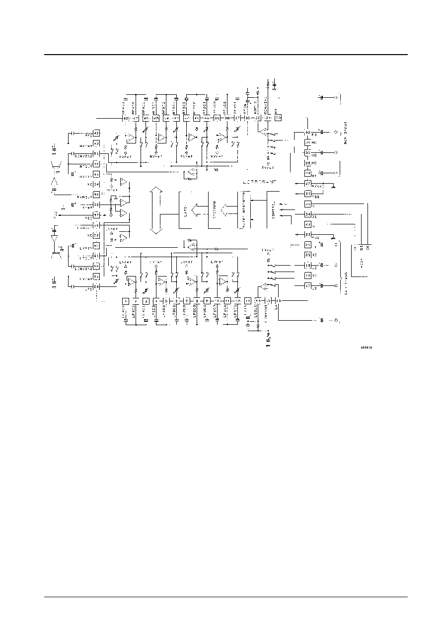
Overview
The LC75394NE is an electronic volume control system
providing control over volume, balance, 5-band equalizer,
and input switching based on serial inputs.
Functions
∑ Volume control:
The chip provides 25 levels of volume attenuation: in 2-
dB steps between 0 dB and ≠20 dB, 3-dB steps between
≠20 dB and ≠32 dB, 4-dB steps between ≠32 dB and ≠52
dB, 4.5-dB steps between ≠52 dB and ≠70 dB, and ≠
.
Independent control over left and right channels
provides balance control.
∑ Equalizer:
The chip provides control in 2-dB steps over the range
between +10 dB and ≠10 dB. Four of the five bands
have peaking equalization; the remaining one, shelving
equalization.
∑ Selector:
The left and right channels each offer a choice of four
inputs. An external constant determines the
amplification for the input signal.
Features
∑ Built-in buffer amplifiers reduce the number of external
parts necessary.
∑ Silicon gate CMOS reduces switching noise.
∑ Serial data input
--Supports CCB* format communication with the
system controller.
∑ A built-in reference voltage circuit divides the supply
voltage (V
DD
) in half.
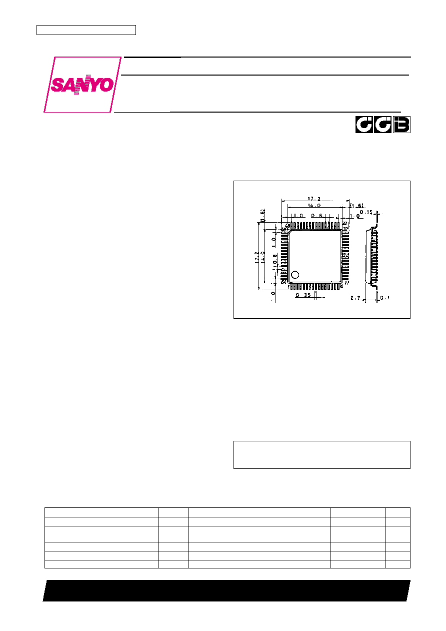
Package Dimensions
unit: mm
3159-QFP64E
CMOS LSI
Ordering number : EN5466
91096HA (OT)/81095HA (OT) No. 5466-1/17
SANYO: QFP64E
[LC75394NE]
SANYO Electric Co.,Ltd. Semiconductor Bussiness Headquarters
TOKYO OFFICE Tokyo Bldg., 1-10, 1 Chome, Ueno, Taito-ku, TOKYO, 110 JAPAN
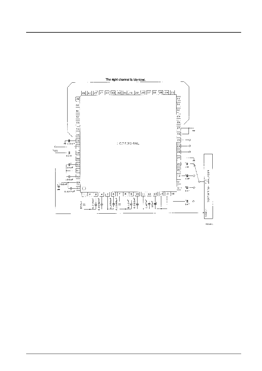
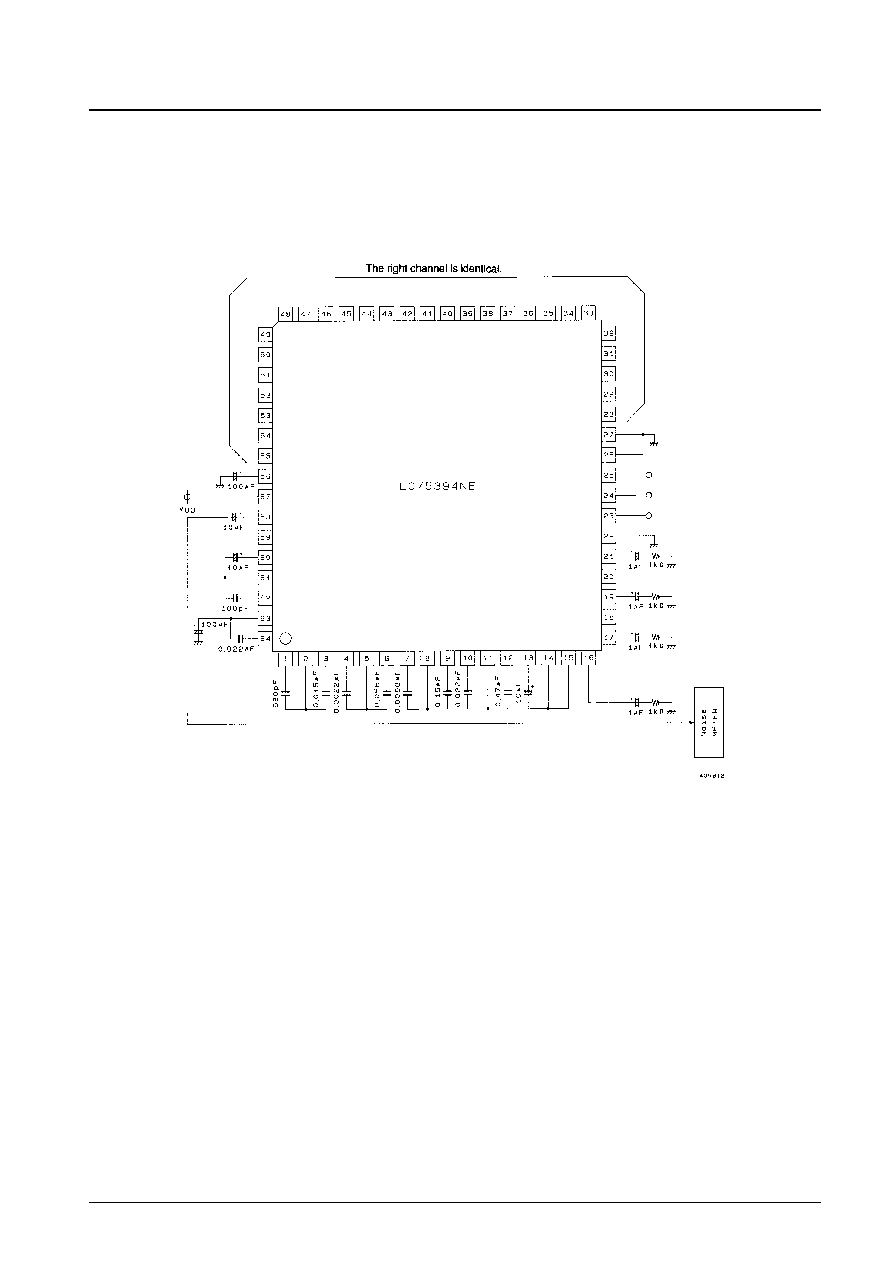
Single-Chip Electronic Volume Control System
LC75394NE
Specifications
Absolute Maximum Ratings
at Ta = 25∞C, V
SS
= 0 V
Parameter
Symbol
Conditions
Ratings
Unit
Maximum supply voltage
V
DD
max
V
DD
12
V
Maximum input voltage
V
IN
max
CL, DI, CE, L1 to L4, R1 to R4, LTIN, RTIN, LVRIN,
V
SS
≠ 0.3 to
V
RVRIN
V
DD
+ 0.3
Allowable power dissipation
Pd max
Ta
85∞C
310
mW
Operating temperature
Topr
≠30 to +85
∞C
Storage temperature
Tstg
≠40 to +125
∞C
∑ CCB is a trademark of SANYO ELECTRIC CO., LTD.
∑ CCB is SANYO's original bus format and all the bus
addresses are controlled by SANYO.
*

Allowable Operating Ranges
at Ta = 25∞C, V
SS
= 0 V
Electrical Characteristics
at Ta = 25∞C, V
DD
= 10 V, V
SS
= 0 V
Input Amplifier Characteristics
at Ta = 25∞C, V
DD
≠ V
SS
= 10 V
No. 5466-2/17
LC75394NE
Parameter
Symbol
Conditions
min
typ
max
Unit
Supply voltage
V
DD
V
DD
6.0
11.0
V
Input high level voltage
V
IH
CL, DI, CE
4.0
V
DD
V
Input low level voltage
V
IL
CL, DI, CE
V
SS
1.0
V
Input voltage amplitude
V
IN
CL, DI, CE, L1 to L4, R1 to R4, LTIN, RTIN, LVRIN,
V
SS
V
DD
Vp-p
RVRIN
Input pulse width
t
¯W
CL
1.0
µs
Setup time
t
SETUP
CL, DI, CE
1.0
µs
Hold time
t
HOLD
CL, DI, CE
1.0
µs
Operating frequency
fopg
CL
500
kHz
Parameter
Symbol
Conditions
min
typ
max
Unit
[Input block]
Input resistance
Rin
L1 to L4, R1 to R4
1
M
Clipping level
Vcl
LSELO, RSELO: THD = 1.0%
2.65
Vrms
Output load resistance
R
L
LSELO, RSELO
3
k
[Volume control block]
Input resistance
Rin
LVRIN, RVRIN
60
100
140
k
[Equalizer control block]
Control range
Geq
Max, boost/cut
±8
±10
±12
dB
Step resolution
Estep
1
2
3
dB
Internal feedback resistance
Rfeed
17
28
39
k
[Overall characteristics]
Total harmonic distortion
THD (1)
V
IN
= 1 Vrms, f = 1 kHz, with all controls flat overall
0.0033
%
THD (2)
V
IN
= 1 Vrms, f = 20 kHz, with all controls flat overall
0.012
%
Crosstalk
CT
V
IN
= 1 Vrms, f = 1 kHz, with all controls flat overall,
86
dB
Rg = 1 k
Output at maximum attenuation
V
O
min
V
IN
= 1 Vrms, f = 1 kHz, main volume ≠
≠90
dB
Output noise voltage
V
N
(1)
With all controls flat overall (IHF-A), Rg = 1 k
3.9
µV
V
N
(2)
With all controls flat overall (DIN-AUDIO), Rg = 1 k
5.4
µV
Current drain
I
DD
V
DD
≠ V
SS
= 11 V
25
33
mA
Input high level current
I
IH
CL, DI, CE, V
IN
= 11 V
10
µA
Input low level current
I
IL
CL, DI, CE, V
IN
= 0 V
≠10
µA
Parameter
Symbol
Conditions
min
typ
max
Unit
Input offset voltage
V
IO
≠10
+10
mV
Input offset current
I
IO
V
SS
V
IN
V
DD
±10
nA
Open-loop voltage gain
A
O
80
dB
Width of 0 dB band
f
T
2.5
MHz
Allowable load resistance
R
L
3
k