Specifications
Absolute Maximum Ratings
at Ta = 25∞C, V
SS
= 0 V
CMOS LSI
Ordering number : EN5056A
63096HA (OT)/71895HA (OT) No. 5056-1/17
SANYO Electric Co.,Ltd. Semiconductor Bussiness Headquarters
TOKYO OFFICE Tokyo Bldg., 1-10, 1 Chome, Ueno, Taito-ku, TOKYO, 110 JAPAN
Single-Chip Electronic Volume Control System
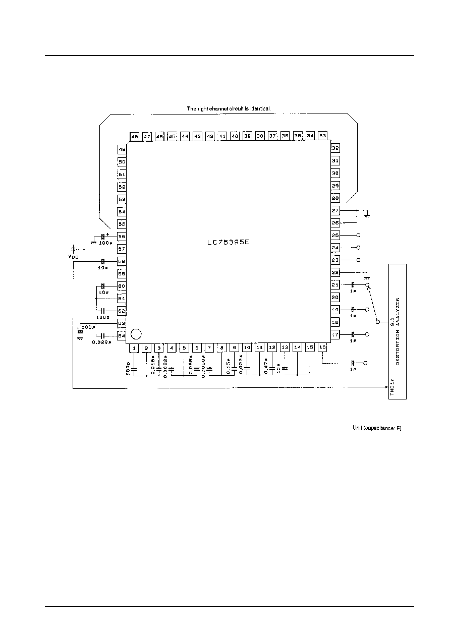
LC75395E
Overview
The LC75395E is an electronic volume control that
provides volume, balance, five-band equalization and
input switching functions. These functions are controlled
from serial input data.
Functions
∑ Volume control: The volume control provides 25
attenuation positions: from 0 dB to ≠17.5 dB in 1.25 dB
steps, from ≠17.5 dB to ≠25 dB in 2.5 dB steps, from
≠25 dB to ≠36.25 dB in 3.75 dB steps and with settings
for ≠41.25 dB, ≠50 dB, ≠60 dB and ≠
.
A balance function can be implemented by controlling
the left and right channels independently.
∑ Equalizer: The equalizer function supports ±10 dB
control in 2 dB steps in each of the five bands. Of the
five bands, four provide peaking characteristics, and one
provides shelving characteristics.
∑ Selector: The selector function selects one of four inputs
for each of the left and right channels. An arbitrary
amplification level can be set for each input signal using
external components.
∑ Serial data input: All controls can be set from serial
input data (CCB format)
Features
∑ On-chip buffer amplifiers to minimize the number of
external components
∑ Silicon-gate CMOS process for minimal switching noise
∑ On-chip circuit to generate the V
DD
/2 reference voltage
Package Dimensions
unit: mm
3159-QFP64E
∑ CCB is a trademark of SANYO ELECTRIC CO., LTD.
∑ CCB is SANYO's original bus format and all the bus
addresses are controlled by SANYO.
Parameter
Symbol
Conditions
Ratings
Unit
Maximum supply voltage
V
DD
max
V
DD
12
V
Maximum input voltage
V
IN
max
CL, DI, CE, L1 to L4, R1 to R4, LTIN, RTIN, LVRIN, RVRIN
V
SS
≠ 0.3 to V
DD
+ 0.3
V
Allowable power dissipation
Pd max
Ta
85∞C
310
mW
Operating temperature
Topr
≠30 to +85
∞C
Storage temperature
Tstg
≠40 to +125
∞C
[LC75395E]
SANYO: QIP64E

Allowable Operating Ranges
at Ta = 25∞C, V
SS
= 0 V
Electrical Characteristics
at Ta = 25∞C, V
DD
= 10 V, V
SS
= 0 V
Input Amplifier Characteristics
at Ta = 25∞C, V
DD
≠ V
SS
= 10 V
No. 5056-2/17
LC75395E
Parameter
Symbol
Conditions
min
typ
max
Unit
Supply voltage
V
DD
V
DD
6.0
11.0
V
Input high level voltage
V
IH
CL, DI, CE
4.0
V
DD
V
Input low level voltage
V
IL
CL, DI, CE
V
SS
1.0
V
Input voltage amplitude
V
IN
CL, DI, CE, L1 to L4, R1 to R4, LTIN, RTIN,
V
SS
V
DD
Vp-p
LVRIN, RVRIN
Input pulse width
t
¯W
CL
1.0
µs
Setup time
t
SETUP
CL, DI, CE
1.0
µs
Hold time
t
HOLD
CL, DI, CE
1.0
µs
Operating frequency
fopg
CL
500
kHz
Parameter
Symbol
Conditions
min
typ
max
Unit
[Input Block]
Input resistance
Rin
L1 to L4, R1 to R4
1
M
Clipping level
Vcl
LSELO, RSELO: THD = 1.0%
2.65
Vrms
Output load resistance
R
L
LSELO, RSELO
3
k
[Volume Control Block]
Input resistance
Rin
LVRIN, RVRIN
21
35
49
k
[Equalizer Control Block]
Control range
Geq
Max, boost/cut
±8
±10
±12
dB
Step resolution
Estep
1
2
3
dB
Internal feedback resistance
Rfeed
17
28
39
k
[Overall Characteristics]
Total harmonic distortion
THD (1)
V
IN
= 1 Vrms, f = 1 kHz, with all controls flat overall
0.0033
%
THD (2)
V
IN
= 1 Vrms, f = 20 kHz, with all controls flat overall
0.012
%
Crosstalk
CT
V
IN
= 1 Vrms, f = 1 kHz, with all controls flat overall
86
dB
Rg = 1 k
Output at maximum attenuation
V
O
min
V
IN
= 1 Vrms, f = 1 kHz, with the main volume
≠84
dB
control at ≠
V
N
(1)
With all controls flat overall (IHF-A), Rg = 1 k
3.9
µV
Output noise voltage
V
N
(2)
With all controls flat overall (DIN-AUDIO),
5.4
µV
Rg = 1 k
Current drain
I
DD
V
DD
≠ V
SS
= 11 V
25
33
mA
Input high level current
I
IH
CL, DI, CE: V
IN
= 11 V
10
µA
Input low level current
I
IL
CL, DI, CE: V
IN
= 0 V
≠10
µA
Parameter
Symbol
Conditions
min
typ
max
Unit
Input offset voltage
V
IO
≠10
+10
mV
Input offset current
I
IO
V
SS
V
IN
V
DD
±10
nA
Open-loop voltage gain
A
O
80
dB
0 dB bandwidth
f
T
2.5
MHz
Allowable load resistance
R
L
3
k