Ordering number : ENN7142
21202TN (OT) No. 7142-1/43
LC75816E, 75816W
SANYO Electric Co.,Ltd. Semiconductor Company
TOKYO OFFICE Tokyo Bldg., 1-10, 1 Chome, Ueno, Taito-ku, TOKYO, 110-8534 JAPAN
1/8 to 1/10 Duty Dot Matrix LCD Display Controllers/Drivers
with Key Input Function
CMOS IC
Any and all SANYO products described or contained herein do not have specifications that can handle
applications that require extremely high levels of reliability, such as life-support systems, aircraft's
control systems, or other applications whose failure can be reasonably expected to result in serious
physical and/or material damage. Consult with your SANYO representative nearest you before using
any SANYO products described or contained herein in such applications.
SANYO assumes no responsibility for equipment failures that result from using products at values that
exceed, even momentarily, rated values (such as maximum ratings, operating condition ranges, or other
parameters) listed in products specifications of any and all SANYO products described or contained
herein.
∑ CCB is a trademark of SANYO ELECTRIC CO., LTD.
∑ CCB is SANYO's original bus format and all the bus
addresses are controlled by SANYO.
Overview
The LC75816E and LC75816W are 1/8 to 1/10 duty dot
matrix LCD display controllers/drivers that support the
display of characters, numbers, and symbols. In addition to
generating dot matrix LCD drive signals based on data
transferred serially from a microcontroller, the LC75816E
and LC75816W also provide on-chip character display ROM
and RAM to allow display systems to be implemented easily.
These products also provide up to 2 general-purpose output
ports and incorporate a key scan circuit that accepts input
from up to 30 keys to reduce printed circuit board wiring.
Features
∑ Key input function for up to 30 keys (A key scan is
performed only when a key is pressed.)
∑ Controls and drives a 5
◊
7, 5
◊
8, or 5
◊
9 dot matrix LCD.
∑ Supports accessory display segment drive (up to 65
segments)
∑ Display technique: 1/8 duty 1/4 bias drive (5
◊
7 dots)
1/9 duty 1/4 bias drive (5
◊
8 dots)
1/10 duty 1/4 bias drive (5
◊
9 dots)
∑ Display digits: 13 digits
◊
1 line (5
◊
7 dots)
12 digits
◊
1 line (5
◊
8 dots, 5
◊
9 dots)
∑ Display control memory
CGROM: 240 characters (5
◊
7, 5
◊
8, or 5
◊
9 dots)
CGRAM: 16 characters (5
◊
7, 5
◊
8, or 5
◊
9 dots)
ADRAM: 13
◊
5 bits
DCRAM: 52
◊
8 bits
∑ Instruction function
Display on/off control
Display shift function
∑ Sleep mode can be used to reduce current drain.
∑ Built-in display contrast adjustment circuit
∑ Switching between the key scan output port and general-
purpose output port functions can be controlled by
instructions.
∑ The frame frequency of the common and segment output
waveforms can be controlled by instructions.
∑ Serial data I/O supports CCB format communication
with the system controller.
∑ Independent LCD driver block power supply VLCD
∑ A voltage detection type reset circuit is provided to
initialize the IC and prevent incorrect display.
∑ The INH pin is provided. This pin turns off the display,
disables key scanning, and forces the general-purpose
output ports to the low level.
∑ RC oscillator circuit
No. 7142-4/43
LC75816E, 75816W
Parameter
Symbol
Conditions
Ratings
Unit
Maximum supply voltage
V
DD
max
V
DD
≠0.3 to +7.0
V
V
LCD
max
V
LCD
≠0.3 to +11.0
V
IN
1
CE, CL, DI, INH
≠0.3 to +7.0
Input voltage
V
IN
2
OSCI, KI1 to KI5, TEST
≠0.3 to V
DD
+ 0.3
V
V
IN
3
V
LCD
1, V
LCD
2, V
LCD
3, V
LCD
4
≠0.3 to V
LCD
+ 0.3
V
OUT
1
DO
≠0.3 to +7.0
Output voltage
V
OUT
2
OSCO, KS1 to KS6, P1, P2
≠0.3 to V
DD
+ 0.3
V
V
OUT
3
V
LCD
0, S1 to S65, COM1 to COM10
≠0.3 to V
LCD
+ 0.3
I
OUT
1
S1 to S65
300
µA
Output current
I
OUT
2
COM1 to COM10
3
I
OUT
3
KS1 to KS6
1
mA
I
OUT
4
P1, P2
5
Allowable power dissipation
Pd max
Ta = 85∞C
200
mW
Operating temperature
Topr
≠40 to +85
∞C
Storage temperature
Tstg
≠55 to +125
∞C
Specifications
Absolute Maximum Ratings
at Ta = 25∞C, V
SS
= 0 V
Parameter
Symbol
Conditions
Ratings
Unit
min
typ
max
V
DD
V
DD
4.5
6.0
Supply voltage
V
LCD
V
LCD
: When the display contrast adjustment circuit is used.
7.0
10.0
V
V
LCD
: When the display contrast adjustment circuit is not used.
4.5
10.0
Output voltage
V
LCD
0
V
LCD
0
V
LCD
4+4.5
V
LCD
V
V
LCD
1
V
LCD
1
3/4 (V
LCD
0
≠
V
LCD
4)
V
LCD
0
Input voltage
V
LCD
2
V
LCD
2
2/4 (V
LCD
0
≠
V
LCD
4)
V
LCD
0
V
V
LCD
3
V
LCD
3
1/4 (V
LCD
0
≠
V
LCD
4)
V
LCD
0
V
LCD
4
V
LCD
4
0
1.5
V
IH
1
CE, CL, DI, INH
0.8 V
DD
6.0
Input high level voltage
V
IH
2
OSCI
0.7 V
DD
V
DD
V
V
IH
3
KI1 to KI5
0.6 V
DD
V
DD
Input low level voltage
V
IL
1
CE, CL, DI, INH, KI1 to KI5
0
0.2 V
DD
V
V
IL
2
OSCI
0
0.3 V
DD
Recommended external resistance
R
OSC
OSCI, OSCO
33
k
Recommended external capacitance
C
OSC
OSCI, OSCO
220
pF
Guaranteed oscillation range
f
OSC
OSC
150
300
600
kHz
Data setup time
t
ds
CL, DI: Figure 2
160
ns
Data hold time
t
dh
CL, DI: Figure 2
160
ns
CE wait time
t
cp
CE, CL: Figure 2
160
ns
CE setup time
t
cs
CE, CL: Figure 2
160
ns
CE hold time
t
ch
CE, CL: Figure 2
160
ns
High level clock pulse width
t¯H
CL: Figure 2
160
ns
Low level clock pulse width
t¯L
CL: Figure 2
160
ns
DO output delay time
t
dc
DO, R
PU
= 4.7k
, C
L
= 10pF
*
1
: Figure 2
1.5
µs
DO rise time
t
dr
DO, R
PU
= 4.7k
, C
L
= 10pF
*
1
: Figure 2
1.5
µs
Allowable Operating Ranges
at Ta = ≠40 to +85∞C, V
SS
= 0 V
Note:
*
1. Since the DO pin is an open-drain output, these times depend on the values of the pull-up resistor R
PU
and the load capacitance C
L
.
No. 7142-5/43
LC75816E, 75816W
Parameter
Symbol
Conditions
Ratings
Unit
min
typ
max
Hysteresis
V
H
CE, CL, DI, INH, KI1 to KI5
0.1 V
DD
V
Power-down detection voltage
V
DET
2.5
3.0
3.5
V
Input high level current
I
IH
CE, CL, DI, INH, OSCI: V
I
= 6.0 V
5.0
µA
Input low level current
I
IL
CE, CL, DI, INH, OSCI: V
I
= 0 V
≠5.0
µA
Input floating voltage
V
IF
KI1 to KI5
0.05 V
DD
V
Pull-down resistance
R
PD
KI1 to KI5: V
DD
= 5.0 V
50
100
250
k
Output off leakage current
I
OFFH
DO: V
O
= 6.0 V
6.0
µA
V
OH
1
S1 to S65: I
O
= ≠20 µA
V
LCD
0 ≠ 0.6
V
OH
2
COM1 to COM10: I
O
= ≠100 µA
V
LCD
0 ≠ 0.6
Output high level voltage
V
OH
3
KS1 to KS6: I
O
= ≠500 µA
V
DD
≠ 1.0
V
DD
≠ 0.5
V
DD
≠ 0.2
V
V
OH
4
P1, P2: I
O
= ≠1 mA
V
DD
≠ 1.0
V
OH
5
OSCO: I
O
= ≠500 µA
V
DD
≠ 1.0
V
OL
1
S1 to S65: I
O
= 20 µA
V
LCD
4 + 0.6
V
OL
2
COM1 to COM10: I
O
= 100 µA
V
LCD
4 + 0.6
Output low level voltage
V
OL
3
KS1 to KS6: I
O
= 25 µA
0.2
0.5
1.5
V
V
OL
4
P1, P2: I
O
= 1 mA
1.0
V
OL
5
OSCO: I
O
= 500 µA
1.0
V
OL
6
DO: I
O
= 1 mA
0.1
0.5
V
MID
1
S1 to S65: I
O
= ±20 µA
2/4 (V
LCD
0 ≠ V
LCD
4) ≠ 0.6
2/4 (V
LCD
0 ≠ V
LCD
4) + 0.6
Output middle level voltage
*
2
V
MID
2
COM1 to COM10: I
O
= ±100 µA
3/4 (V
LCD
0 ≠ V
LCD
4) ≠ 0.6
3/4 (V
LCD
0 ≠ V
LCD
4) + 0.6
V
V
MID
3
COM1 to COM10: I
O
= ±100 µA
1/4 (V
LCD
0 ≠ V
LCD
4) ≠ 0.6
1/4 (V
LCD
0 ≠ V
LCD
4) + 0.6
Oscillator frequency
f
OSC
OSCI, OSCO: R
OSC
= 33 k
, C
OSC
= 220 pF
210
300
390
kHz
I
DD
1
V
DD
: sleep mode
100
I
DD
2
V
DD
: V
DD
= 6.0 V, output open, f
OSC
= 300 kHz
500
1000
Current drain
I
LCD
1
V
LCD
: sleep mode
5
µA
I
LCD
2
V
LCD
: V
LCD
= 10.0 V, output open, f
OSC
= 300 kHz
450
900
When the display contrast adjustment circuit is used.
I
LCD
3
V
LCD
: V
LCD
= 10.0 V, output open, f
OSC
= 300 kHz
200
400
When the display contrast adjustment circuit is not used.
Electrical Characteristics
for the Allowable Operating Ranges
Note:
*
2. Excluding the bias voltage generation divider resistor built into the V
LCD
0, V
LCD
1, V
LCD
2, V
LCD
3, and V
LCD
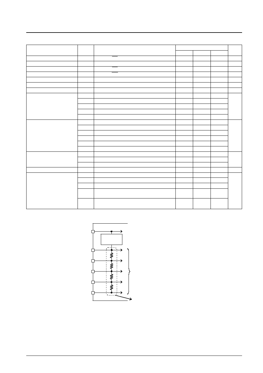
4. (See Figure 1.)
VLCD
VLCD3
VLCD4
VLCD2
VLCD0
VLCD1
CONTRAST
ADJUSTER
Excluding these resistors
To the common and segment drivers
Figure 1