 | –≠–ª–µ–∫—Ç—Ä–æ–Ω–Ω—ã–π –∫–æ–º–ø–æ–Ω–µ–Ω—Ç: LC75821E | –°–∫–∞—á–∞—Ç—å:  PDF PDF  ZIP ZIP |

Ordering number : EN4532C
432
22898HA(OT)/12395TH(KOTO)/N1093(KOTO) No. 4532-1/10
LC75821E, 75821W
SANYO Electric Co.,Ltd. Semiconductor Bussiness Headquarters
TOKYO OFFICE Tokyo Bldg., 1-10, 1 Chome, Ueno, Taito-ku, TOKYO, 110-0005 JAPAN
LCD Display Drivers
CMOS LSI
Overview
The LC75821E and LC75821W are general-purpose LCD
display drivers that can be used for frequency display in
microprocessor-controlled radio receivers and in other
display applications.
Features
∑ 53 segment outputs (the maximum for static drive)
∑ Two drive types: static (1/1) duty (53 segments) and 1/2
duty (104 segments)
∑ Data input: 3 serial input pins
∑ INH pin for turning off all display output
∑ The difference form the LC7582: The LC75821E,
LC75821W are A/D converter, DSP function-removed
versions of the LC7582 of which the functions other
than the two can be used with pin compatibility with
the LC7582 kept.
Package Dimensions
unit: mm
3159-QFP64E
unit: mm
3190-SQFP64
1
16
17
32
33
48
49
64
1.0
14.0
17.2
1.0
1.0
1.6
0.15
0.35
0.1
15.6
0.8
0.8
3.0max
2.7
14.0
17.2
1.0
1.6
0.8
SANYO: QIP64E
[LC75821E]
10.0
12.0
1.25
0.5
1.25
1.25
0.5
1.25
0.18
12.0
10.0
0.5
1.7max
0.5
0.1
0.15
1
16
17
32
33
48
49
64
SANYO: SQFP64
[LC75821W]

Specifications
Absolute Maximum Ratings
at Ta = 25∞C, V
SS
= 0 V
Allowable Operating Ranges
at Ta = ≠40 to +85∞C, V
SS
= 0 V
Electrical Characteristics
for the Allowable Operating Ranges
No. 4532-2/10
LC75821E, 75821W
Parameter
Symbol
Conditions
Ratings
Unit
Maximum supply voltage
V
DD
max
V
DD
≠0.3 to +7.0
V
V
LCD
V
LCD
≠0.3 to V
DD
+ 0.3
V
Input voltage
V
IN
1
CE, CLK, DATA, INH
≠0.3 to +7.0
V
V
IN
2
OSC: output off
≠0.3 to V
DD
+ 0.3
V
Output voltage
V
OUT
OSC: output off
≠0.3 to V
DD
+ 0.3
V
Output current
I
OUT
1
S1 to S53
100
µA
I
OUT
2
COM1, COM2
1.0
mA
Allowable power dissipation
Pd max
Ta = 85∞C
100
mW
Operating temperature
Topr
≠40 to +85
∞C
Storage temperature
Tstg
≠55 to +125
∞C
Parameter
Symbol
Conditions
min
typ
max
Unit
Supply voltage
V
DD
V
DD
3.0
6.5
V
V
LCD
V
LCD
3.0
V
DD
V
Input high-level voltage
V
IH
1
INH
0.7 V
DD
6.5
V
Input high-level voltage
V
IH
2
CE, CLK, DATA
0.8 V
DD
6.5
V
Input low-level voltage
V
IL
1
INH
0
0.3 V
DD
V
Input low-level voltage
V
IL
2
CE, CLK, DATA
0
0.2 V
DD
V
Recommended external
R
OSC
OSC
51
k
resistance
Recommended external
C
OSC
OSC
680
pF
capacitance
Guaranteed oscillation range
f
OSC
OSC
25
50
100
kHz
Clock low-level pulse width
t
¯L
CLK
0.25
µs
Clock high-level pulse width
t
¯H
CLK
0.25
µs
Data setup time
t
sup
CLK, DATA
0.25
µs
Data hold time
t
dh
CLK, DATA
0.25
µs
t
1
CE, DATA
1
µs
Serial data pulse width
t
2
CE, CLK
1.25
µs
t
3
1
µs
t
4
4
µs
Parameter
Symbol
Conditions
min
typ
max
Unit
Input high-level current
I
IH
CE, CLK, DATA, INH: V
I
= 6.5 V
5
µA
Input low-level current
I
IL
CE, CLK, DATA, INH: V
I
= 0 V
≠5
µA
Output high-level voltage
V
OH
1
S1 to S53: I
O
= ≠10 µA
V
DD
≠ 1.0
V
Output high-level voltage
V
OH
2
COM1, COM2: I
O
= ≠100 µA
V
LCD
≠ 0.6
V
Output low-level voltage
V
OL
1
S1 to S53: I
O
= 10 µA
1.0
V
Output low-level voltage
V
OL
2
COM1, COM2: I
O
= 100 µA
0.6
V
Mid-level voltage
V
MID
1
COM1, COM2: V
LCD
= 6.5 V, I
O
= ±100 µA
2.65
3.25
3.85
V
V
MID
2
COM1, COM2: V
LCD
= 3.0 V, I
O
= ±100 µA
0.9
1.5
2.1
V
Oscillator frequency
f
OSC
OSC: R = 51 k
, C = 680 pF
40
50
60
kHz
Hysteresis voltage
V
H
CE, CLK, DATA: V
DD
= 5 V
0.3
V
Current drain
I
DD
0.6
mA
I
LCD
V
LCD
2
mA
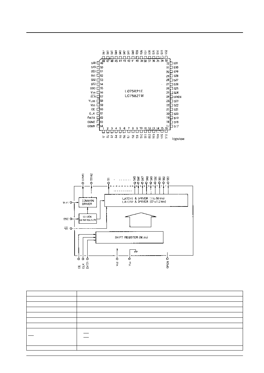
Pin Assignment
Block Diagram
Pin Functions
No. 4532-3/10
LC75821E, 75821W
Pin
Function
S1 to S53
Segment output pins
COM1, COM2
Common output pins (Only COM1 is used in static (1/1) drive. COM2 must be left open in that mode.)
V
LCD
LCD bias voltage setting
OSC
Oscillator connection
CE, CLK, DATA
Serial data transfer inputs
V
SS
, V
DD
Power supply
Display off control input
INH
INH = low (V
SS
) ..........Display off (S1 to S53, COM1, COM2 = low)
INH = high (V
DD
).........Display on
Note that serial data transfers can be performed when display output is forced off.
OPEN
Make no connections to this pin.

Data Transfer Format
1. Static (1/1) duty
2. 1/2 duty (Only 56 bits need to be transferred if there are no more than 52 display segments. The transfer format is
identical to the static duty case. It is not possible to change the D54 to D106 data without specifying the D1 to D53
data.)
D1 to D53:
Display data (1/1 duty) Lighted at 1
D1 to D106: Display data (1/2 duty) Unlighted at 0
DP:
Drive type selection bit
1/2 duty at 1
1/1 duty at 0
◊
:
don't care
Data Transfer Examples
1. Static duty
2. 1/2 duty with 52 or fewer segments
3. 1/2 duty with more than 52 segments
Note: The following transfer format is not allowed in 1/2 duty with 52 or fewer segments.
No. 4532-4/10
LC75821E, 75821W
Transfer direction (56 bits)
Transfer direction (112 bits)
The values of bits D53 and D106 are ignored.(don't care)

Serial Data
1. Static duty (56 bits)
2. 1/2 duty (112 bits)
Output Waveforms
1. Static duty
No. 4532-5/10
LC75821E, 75821W
Internal latch 1
Internal latch 1
Internal latch 2
Segment off period
Segment on period