 | –≠–ª–µ–∫—Ç—Ä–æ–Ω–Ω—ã–π –∫–æ–º–ø–æ–Ω–µ–Ω—Ç: LC78621E | –°–∫–∞—á–∞—Ç—å:  PDF PDF  ZIP ZIP |
CMOS LSI
Ordering number : EN
*
5223
83095HA (OT) No. 5223-1/34
Preliminary
SANYO Electric Co.,Ltd. Semiconductor Bussiness Headquarters
TOKYO OFFICE Tokyo Bldg., 1-10, 1 Chome, Ueno, Taito-ku, TOKYO, 110-8534 JAPAN
Compact Disc Player DSP
LC78621E
Overview
The LC78621E is a CMOS LSI that implements the signal
processing and servo control required by compact disk
players, laser disks, CD-V, CD-I and related products. The
LC78621E provides several types of signal processing,
including demodulation of the optical pickup EFM signal,
de-interleaving, error detection and correction, and digital
filters that can help reduce the cost of CD player units. It
also processes a rich set of servo system commands sent
from the control microprocessor. It also incorporates an
EFM-PLL circuit and a one-bit D/A converter.
Functions
∑ Input signal processing: The LC78621E takes an HF
signal as input, digitizes (slices) that signal at a precise
level, converts that signal to an EFM signal, and
generates a PLL clock with an average frequency of
4.3218 MHz by comparing the phases of that signal and
an internal VCO.
∑ Precise reference clock and necessary internal timing
generation using an external 16.9344 MHz crystal
oscillator
∑ Disk motor speed control using a frame phase difference
signal generated from the playback clock and the
reference clock
∑ Frame synchronization signal detection, protection and
interpolation to assure stable data readout
∑ EFM signal demodulation and conversion to 8-bit
symbol data
∑ Subcode data separation from the EFM demodulated
signal and output of that data to an external
microprocessor
∑ Subcode Q signal output to a microprocessor over the
serial I/O interface after performing a CRC error check
∑ Demodulated EFM signal buffering in internal RAM to
handle up to ±4 frames of disk rotational jitter
∑ Demodulated EFM signal reordering in the prescribed
order for data unscrambling and de-interleaving
∑ Error detection, correction, and flag processing (error
correction scheme: dual C1 plus dual C2 correction)
∑ The LC78620E sets the C2 flags based on the C1 flags
and a C2 check, and then performs signal interpolation
or muting depending on the C2 flags. The interpolation
circuit uses a quadruple interpolation scheme. The
output value converges to the muting level when four or
more consecutive C2 flags occur.
∑ Support for command input from a control
microprocessor: commands include track jump, focus
start, disk motor start/stop, muting on/off and track
count (8 bit serial input)
∑ Built-in digital output circuits.
∑ Arbitrary track counting to support high-speed data
access
∑ Zero cross muting
∑ Supports the implementation of a double-speed dubbing
function.
∑ D/A converter outputs with data continuity improved by
8
◊
oversampling digital filters. (These filters function as
4
◊
oversampling filters during double-speed playback.)
∑ Built-in third-order
D/A converters (PWM output)
∑ Built-in digital attenuator (8 bits ≠ alpha, 239 steps)
∑ Built-in digital de-emphasis
∑ Built-in digital level and peak meter functions
∑ Support for bilingual applications
Features
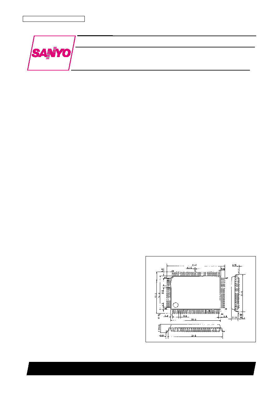
∑ 80-pin QIP (miniature, reduced space package)
∑ Silicon gate CMOS process (for low power)
∑ 5 V single-voltage power supply (for use in portable
products)
Package Dimensions
unit: mm
3174-QFP80E
SANYO: QIP80E
[LC78621E]
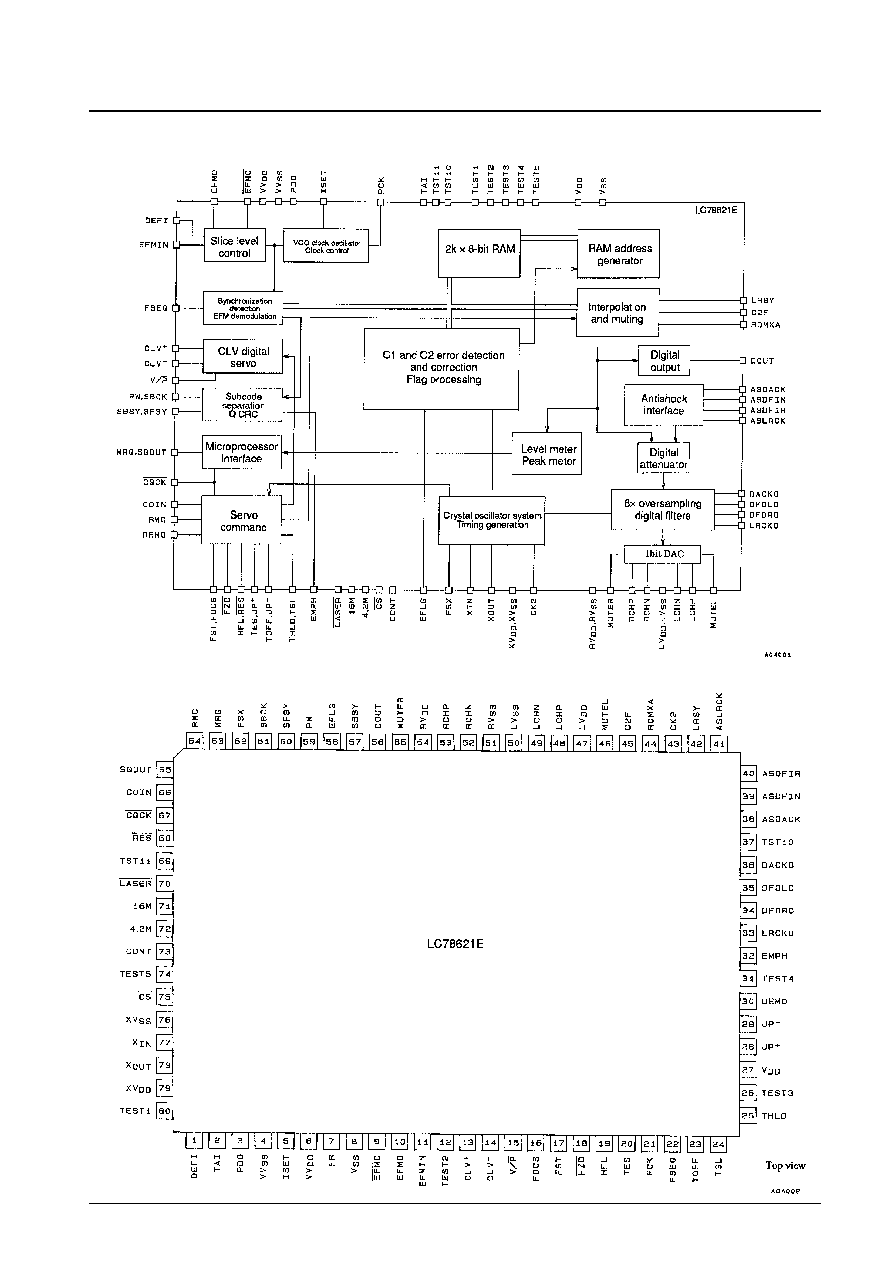
Equivalent Circuit Block Diagram
Pin Assignment
No. 5223-2/34
LC78621E
Specifications
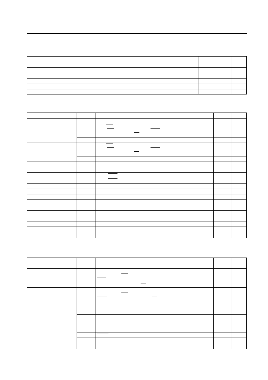
Absolute Maximum Ratings
at Ta = 25∞C, V
SS
= 0 V
Allowable Operating Ranges
at Ta = 25∞C, V
SS
= 0 V
Note: Due to the structure of this LSI, an identical voltage must be supplied to all the power supply pins.
Electrical Characteristics
at Ta = 25∞C, V
DD
= 5 V, V
SS
= 0 V
No. 5223-3/34
LC78621E
Parameter
Symbol
Conditions
Ratings
Unit
Maximum supply voltage
V
DD
max
V
SS
≠ 0.3 to V
SS
+ 7.0
V
Maximum input voltage
V
IN
max
V
SS
≠ 0.3 to V
DD
+ 0.3
V
Maximum output voltage
V
OUT
max
V
SS
≠ 0.3 to V
DD
+ 0.3
V
Allowable power dissipation
Pd max
300
mW
Operating temperature
Topr
≠20 to +75
∞C
Storage temperature
Tstg
≠40 to +125
∞C
Parameter
Symbol
Conditions
min
typ
max
Unit
Supply voltage
V
DD
V
DD
, XV
DD
, LV
DD
, RV
DD
, VV
DD
3.6
5.5
V
DEFI, FZD, ASDACK, ASDFIN, ASDFIR, ASLRCK,
Input high-level voltage
V
IH
(1)
COIN, RES, HFL, TES, SBCK, RWC, CQCK, TAI,
0.7 V
DD
V
DD
V
TEST1 to TEST5, DEMO, CS
V
IH
(2)
EFMIN
0.6 V
DD
V
DD
V
DEFI, FZD, ASDACK, ASDFIN, ASDFIR, ASLRCK,
Input low-level voltage
V
IL
(1)
COIN, RES, HFL, TES, SBCK, RWC, CQCK, TAI,
0
0.3 V
DD
V
TEST1 to TEST5, DEMO, CS
V
IL
(2)
EFMIN
0
0.4 V
DD
V
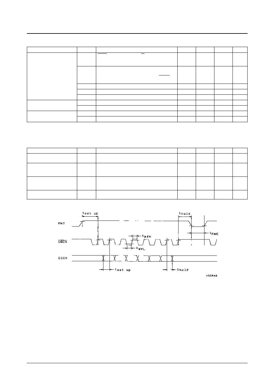
Data setup time
t
set up
COIN, RWC: Figure 1
400
ns
Data hold time
t
hold
COIN, RWC: Figure 1
400
ns
High-level clock pulse width
t
W¯H
SBCK, CQCK: Figures 1, 2 and 3
400
ns
Low-level clock pulse width
t
W¯L
SBCK, CQCK: Figures 1, 2 and 3
400
ns
Data read access time
t
RAC
SQOUT, PW: Figures 2 and 3
0
400
ns
Command transfer time
t
RWC
RWC: Figure 1
1000
ns
Subcode Q read enable time
t
SQE
WRQ: Figure 2, with no RWC signal
11.2
ms
Subcode read cycle
t
sc
SFSY: Figure 3
136
µs
Subcode read enable time
t
se
SFSY: Figure 3
400
ns
Input level
V
IN
(1)
EFMIN
1.0
Vp-p
V
IN
(2)
X
IN
: Input capacitor coupled
1.0
Vp-p
Operating frequency range
fop
EFMIN
10
MHz
Crystal oscillator frequency
fX (1)
X
IN
, X
OUT
: In 16M mode
16.9344
MHz
fX (2)
X
IN
, X
OUT
: In 32M mode
33.8688
MHz
Parameter
Symbol
Conditions
min
typ
max
Unit
Current drain
I
DD
30
45
mA
DEFI, EFMIN, FZD, ASDACK, ASDFIN, ASDFIR,
Input high-level current
I
IH
(1)
ASLRCK, COIN, RES, HFL, TES, SBCK, RWC,
5
µA
CQCK: V
IN
= 5 V
I
IH
(2)
TAI, TEST1 to TEST5, DEMO, CS: V
IN
= V
DD
= 5.5 V
25
75
µA
DEFI, EFMIN, FZD, ASDACK, ASDFIN, ASDFIR,
Input low-level current
I
IL
ASLRCK, COIN, RES, HFL, TES, SBCK, RWC,
≠5
µA
CQCK, TAI, TEST1 to TEST5, DEMO, CS: V
IN
= 0 V
EFMO, EFMO, CLV
+
, CLV
≠
, V/P, FOCS, PCK, FSEQ,
V
OH
(1)
TOFF, TGL, THLD, JP
+
, JP
≠
, EMPH, EFLG, FSX:
4
V
I
OH
= ≠1 mA
MUTEL, MUTER, LRCKO, DFORO, DFOLO, DACKO,
V
OH
(2)
TST10, LRSY, CK2, ROMXA, C2F, SBSY, PW, SFSY,
4
V
Output high-level voltage
WRQ, SQOUT, TST11, 16M, 4.2M, CONT:
I
OH
= ≠0.5 mA
V
OH
(3)
LASER: I
OH
= ≠1 mA
4.6
V
V
OH
(4)
DOUT: I
OH
= ≠12 mA
4.5
V
V
OH
(5)
LCHP, RCHP, LCHN, RCHN: I
OH
= ≠1mA
3.0
4.5
V
Continued on next page.
Continued from preceding page.
Note: For guaranteed operation, the VCO oscillator frequency range adjustment resistor FR must be a 1.20 k
(±5.0%) tolerance resistor.
One-Bit D/A Converter Analog Characteristics
at Ta = 25∞C, V
DD
= LV
DD
= RV
DD
= 5 V, V
SS
= LV
SS
= RV
SS
= 0 V
Note: Measured with the normal-speed playback mode in the Sanyo one-bit D/A converter block reference digital attenuator circuit set to EE (hexadecimal).
Figure 1 Command Input
No. 5223-4/34
LC78621E
Parameter
Symbol
Conditions
min
typ
max
Unit
Total harmonic distortion
THD + N
LCHP, RCHP, LCHN, RCHN; 1 kHz: 0 dB data input,
0.008
0.010
%
using the 20 kHz low-pass filter (AD725D built in)
LCHP, RCHP, LCHN, RCHN; 1 kHz: ≠60 dB data input,
Dynamic range
DR
using the 20 kHz low-pass filter and the A filter
84
88
dB
(AD725D built in)
LCHP, RCHP, LCHN, RCHN; 1 kHz: 0 dB data input,
Signal-to-noise ratio
S/N
using the 20 kHz low-pass filter and the A filter
98
100
dB
(AD725D built in)
Crosstalk
CT
LCHP, RCHP, LCHN, RCHN; 1 kHz: 0 dB data input,
96
98
dB
using the 20 kHz low-pass filter (AD725D built in)
Parameter
Symbol
Conditions
min
typ
max
Unit
EFMO, EFMO, CLV
+
, CLV
≠
, V/P, FOCS, PCK, FSEQ,
V
OL
(1)
TOFF, TGL, THLD, JP
+
, JP
≠
, EMPH, EFLG, FSX:
1
V
I
OL
= 1 mA
MUTEL, MUTER, LRCKO, DFORO, DFOLO, DACKO,
V
OL
(2)
TST10, LRSY, CK2, ROMXA, C2F, SBSY, PW, SFSY,
0.4
V
Output low-level voltage
WRQ, SQOUT, TST11, 16M, 4.2M, CONT, LASER:
I
OL
= 2 mA
V
OL
(3)
DOUT: I
OL
= 12 mA
0.5
V
V
OL
(4)
FST: I
OL
= 5 mA
0.75
V
V
OL
(5)
LCHP, RCHP, LCHN, RCHN: I
OL
= 1mA
0.5
2.0
V
Output off leakage current
I
OFF
(1)
PDO, CLV
+
, CLV
≠
, JP
+
, JP
≠
, FST: V
OUT
= 5 V
5
µA
I
OFF
(2)
PDO, CLV
+
, CLV
≠
, JP
+
, JP
≠
: V
OUT
= 0 V
≠5
µA
Charge pump output current
I
PDOH
PDO: R
ISET
= 68 k
100
125
150
µA
I
PDOL
PDO: R
ISET
= 68 k
≠150
≠125
≠100
µA
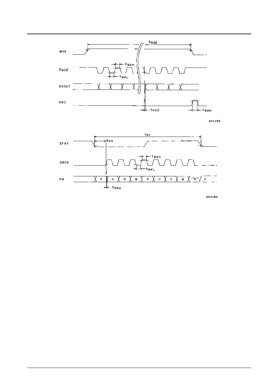
Figure 2 Subcode Q Output
Figure 3 Subcode Output
No. 5223-5/34
LC78621E