 | –≠–ª–µ–∫—Ç—Ä–æ–Ω–Ω—ã–π –∫–æ–º–ø–æ–Ω–µ–Ω—Ç: LC78845Q | –°–∫–∞—á–∞—Ç—å:  PDF PDF  ZIP ZIP |
Ordering number : EN
*
5236
22896HA (OT) No. 5236-1/10
Overview
The LC78845Q is a synchronous sample rate converter for
digital audio signals.
Features
∑ Converts data sampled at 32 or 48 kHz to 44.1-kHz
sampled data.
∑ Passes 44.1-kHz sampled data trough without change.
∑ Supports 384fs and 512fs system clock rates.
∑ 8
◊
oversampling filters
∑ Soft muting function
∑ Built-in PLL circuit
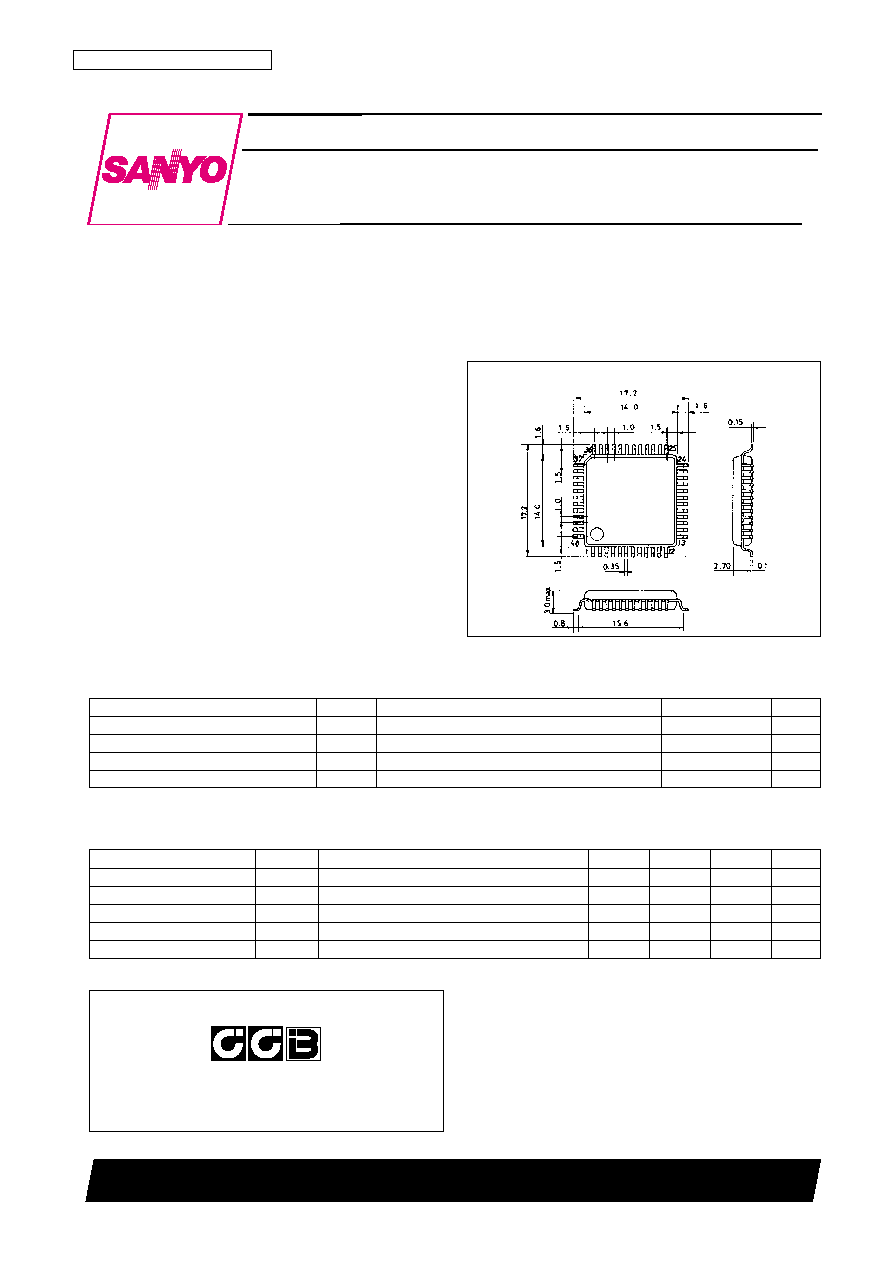
Package Dimensions
unit: mm
3156-QFP48E
Preliminary
SANYO: QIP48E
[LC78845Q]
LC78845Q
SANYO Electric Co.,Ltd. Semiconductor Bussiness Headquarters
TOKYO OFFICE Tokyo Bldg., 1-10, 1 Chome, Ueno, Taito-ku, TOKYO, 110-0005 JAPAN
Sample Rate Converter for Digital Audio
CMOS LSI
This LSI can easily use CCB that is SANYO's original bus format.
∑ CCB is a trademark of SANYO ELECTRIC CO., LTD.
∑ CCB is SANYO's original bus format and all the bus
addresses are controlled by SANYO.
Specifications
Absolute Maximum Ratings
at Ta = 25∞C
DC Characteristics
Parameter
Symbol
Conditions
Ratings
Unit
Maximum supply voltage
V
DD
max
≠0.3 to +7.0
V
I/O voltages
V
I
, V
O
≠0.3 to V
DD
+ 0.3
V
Operating temperature
Topr
≠30 to +70
∞C
Storage temperature
Tstg
≠55 to +125
∞C
Parameter
Symbol
Conditions
min
typ
max
Unit
Input voltage range
V
IN
Ta = ≠30 to +70∞C
0
V
DD
V
Input high-level voltage
V
IH
0.7 V
DD
V
Input low-level voltage
V
IL
0.3 V
DD
V
Output high-level voltage
V
OH
I
OH
= ≠1 µA
V
DD
≠ 0.05
V
Output low-level voltage
V
OL
I
OL
= 1 µA
V
SS
+ 0.05
V
AC Characteristics
1. Audio data input
2. Audio data output
No. 5236-2/10
LC78845Q
Parameter
Symbol
Conditions
min
typ
max
Unit
BCLKI pulse width
t
BKW
50
ns
DATAI setup time
t
DS
20
ns
DATAI hold time
t
DH
20
ns
LRCKI hold time
t
LH
25
ns
LRCKI setup time
t
LS
25
ns
Parameter
Symbol
Conditions
min
typ
max
Unit
BCLKO pulse width
t
BWO
100
ns
DATAO output delay time
t
DAD
25
ns
DATAO setup time
t
DSO
50
ns
DATAO hold time
t
DHO
50
ns
LRCKO output delay time
t
LRD
25
ns
LRCKO setup time
t
LSO
50
ns
LRCKO hold time
t
LHO
50
ns
WCLKO setup time
t
WSO
50
ns
WCLKO hold time
t
WHO
50
ns
3. Serial input (CCB = low)
4. Serial input (CCB = high)
No. 5236-3/10
LC78845Q
Parameter
Symbol
Conditions
min
typ
max
Unit
CL pulse width
t
CLW
50
ns
DI setup time
t
DS
20
ns
DI hold time
t
DH
20
ns
CE pulse width
t
CEW
50
ns
CE setup time
t
CS
20
ns
CE hold time
t
CH
20
ns
DO0 to DO7 output delay time
t
DOD
25
ns
Parameter
Symbol
Conditions
min
typ
max
Unit
CL pulse width
t
CLW
50
ns
DI setup time
t
DS
20
ns
DI hold time
t
DH
20
ns
CE setup time
t
CS
20
ns
CE hold time
t
CH
20
ns
DO0 to DO7 output delay time
t
DOD
25
ns
with respect to the rise of CE
Pin Assignment
Although the DV
DD
and AV
DD
pins in this IC are given different names to correspond to the internal circuit structure,
they are connected internally through the circuit substrate. As a result, if different voltages are applied to these pins,
abnormal currents will flow in the chip. Since this can cause latchup, power supplies with identical voltages and identical
power-on timings must be used.
Pin Functions
No. 5236-4/10
LC78845Q
Pin No.
Symbol
Overview
Function
1
2
3
4
5
6
7
8
9
10
11
MKSEL
INITB
MCK1
BCLKI
DGND
DGND
DV
DD
LRCKI
DATAI
CCB
SPSEL
DF master clock selection
Reset input
DF master clock input
Audio signal input
Digital system ground
Digital system ground
Digital system power supply
Audio signal input
Serial input format specification
Serial/parallel control
Low: 384fs, high: 512fs
Low: initialization operation
Audio signal bit clock input pin
Audio signal left/right clock and data input pins
Selects the input format for data from the microprocessor input pins.
Allows certain of the setting pins to be set from serial data over the
microprocessor interface.
Low: serial, high: parallel (states set by input pins)
Continued on next page.
Continued from preceding page.
No. 5236-5/10
LC78845Q
Pin No.
Symbol
Overview
Function
12
13
14
15
16
17
18
19
20
21
22
23
24
25
26
27
28
29
30
31
32
33
34
35
36
37
38
39
40
41
42
43
44
45
46
47
48
CE
CL
DI
DO7
DO6
DO5
DGND
DV
DD
DO4
DO3
DO2
DO1
DO0
DATAO
LRCKO
WCLKO
BCLKO
DGND
N.C
AGND
VCO
VIN
R
STOP
UNLK
MCK2
AV
DD
AV
DD
MUTE
FSEL3
TEST1
DV
DD
DV
DD
FSEL2
FSEL1
TEST2
TEST3
Microprocessor input pins
Parallel data output
Digital system ground
Digital system power supply
Parallel data output
Audio signal output
Digital system ground
--
Analog system ground
PLL control
PLL control
PLL control
Oscillator stop signal input
Unlock detection output
Synchronization clock output
Analog system power supply
Analog system power supply
Muting
Output data fs selection
Test pin
Digital system power supply
Digital system power supply
Input signal fs selection
Test pins
Data enable signal input
Shift clock input
Address/data input
Output of 8-bit parallel data according to microprocessor input
Output of 8-bit parallel data according to microprocessor input
Audio signal outputs (data, left/right clock, word clock, and bit clock)
Low-pass filter connection
Free-running setting
VCO band adjustment
Low: oscillator stopped, high: PLL running
Outputs a high level when the PLL circuit is unlocked.
Outputs the clock generated by the VCO.
Low: muting off, high: muting on
Low: fs data, high: 2fs data
Must be held low during normal operation.
Selects the fs for the input signal.
Must be held low during normal operation.