LC7940YC,7941YC
SANYO Electric Co., Ltd. Semiconductor Company
TOKYO OFFICE Tokyo Bldg., 1-10, 1 Chome, Ueno, Taito-ku, TOKYO, 110-8534 JAPAN
63099RM (ID) No. 6157--1/13
Ordering number: EN 6157
s
Any and all SANYO products described or contained herein do not have specifications that can handle
applications that require extremely high levels of reliability, such as life-support systems, aircraft's
control systems, or other applications whose failure can be reasonably expected to result in serious
physical and/or material damage. Consult with your SANYO representative nearest you before using
any SANYO products described or contained herein in such applications.
s
SANYO assumes no responsibility for equipment failures that result from using products at values that
exceed, even momentarily, rated values (such as maximum ratings, operating condition ranges, or other
parameters) listed in products specifications of any and all SANYO products described or contained
herein.
CMOS IC
Dot-matrix LCD Drivers
Overview
The LC7940YC and LC7941YC are segment driver ICs
for driving large, dot
≠
matrix LCD displays. They read 4
≠
bit parallel or serial input, display data from a controller
into an 80
≠
bit latch, and then generate LCD drive signals
corresponding to that data.
The LC7940YC and LC7941YC feature mirror
≠
image pin
assignments, allowing them to be used together to increase
component density. They are designed to be used with the
LC7942YC common driver to drive large LCD panels.
Features
∑ 80 built
≠
in LCD display drive circuits
∑ 1/8 to l/128 display duty cycle
∑ Serial or 4
≠
bit parallel data input
∑ Chip disable for low power dissipation for large
≠
sized
panels
∑ Bias supply voltags can be supplied externally
∑ Operating supply voltage and ambient temperature
- 2.7 to 5.5 V logic supply ( V
DD
) at Ta =
≠
20 to +85∞C
- 8 to 20V LCD supply (V
DD
≠
V
EE
) at Ta =
≠
20 to
+85 ∞C
∑ CMOS process
Specifications
The following electrical characteristics apply when sealed in a Sanyo standard QIC-100 package.
Absolute Maximum Ratings
at Ta = 25 ± 2∞C, V
SS
= 0 V
Parameter
Symbol
Ratings
Unit
Logic supply voltge
V
DD
max
≠0.3 to +7.0
V
LCD supply voltage, See Note below.
V
DD
≠ V
EE
max
0 to 22
V
Input voltage
V
I
max
≠0.3 to V
DD
+ 03
∞C
LC7940YC, LC7941YC
No. 6157--2/13
Note
V
DD
V
1
> V
3
> V
4
> V
EE
Recommended Operating Condltions
at Ta =
≠
20 to + 85∞C, V
SS
= 0V
Notes
1. V
DD
V
l
> V
3
> V
4
> V
EE
2. At turn ON, the LCD supply should be energized after or simultaneously with the logic supply. At turn OFF, the logic supply
should be cut after or simultaneously with the LCD supply.
Electrlcai Characterfstlcs
at Ta = 25 ± 2∞C,V
SS
= 0V, V
DD
= 2.7 to 5.5 V
Operating temperature range
T
opr
≠20 to +85
∞C
Storage temperature range
T
stg
≠40 to +125
∞C
Parameter
Symbol
Conditions
Ratings
Unit
min
typ
max
Logic supply voltage
V
DD
2.7
≠
5.5
V
LCD supply voltage
V
DD
≠ V
EE
See Notes 1 and 2.
8
≠
20
V
HIGH≠level input voltage
V
IH
CP, CDl, DI1 to DI3, M,
SDl, P/S, DISPOFF and
LOAD
0.8V
DD
≠
≠
V
LOW≠level inpvt voltage
V
IL
CP, CDI, Dl1 to DI3, M,
SDl, P/S,DISPOFF and
LOAD
≠
≠
0.2V
DD
V
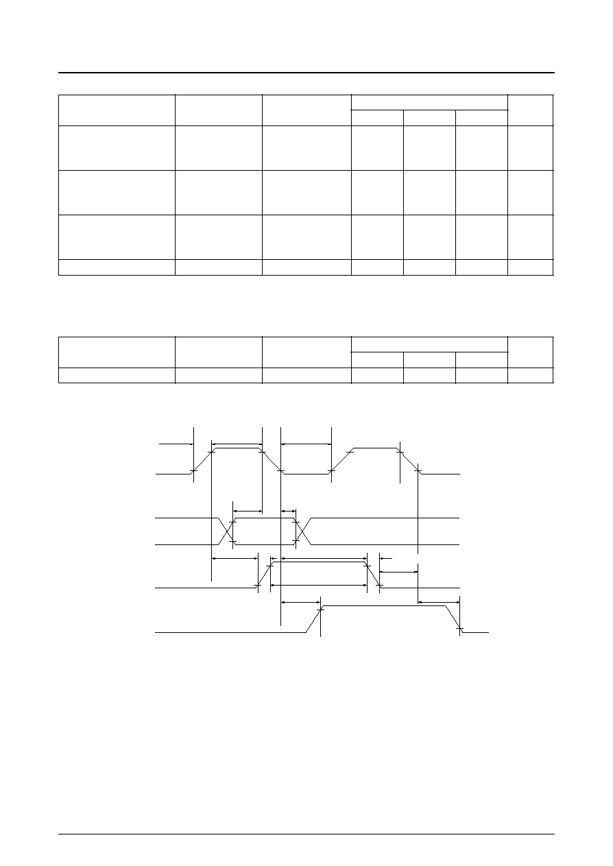
CP shift clock frequency
f
CP
≠
3.3
MHz
CP pulsewidth
t
WC
100
≠
≠
ns
LOAD pulsewidth
t
WL
100
≠
≠
ns
DIn and SDI to CP setup time
t
SETUP
80
≠
≠
ns
DIn and SDI to CP hold time
t
HOLD
80
≠
≠
ns
CP to LOAD time
t
CL1
0
≠
≠
ns
t
CL2
100
≠
≠
ns
LOAD to CP time
t
LC
100
≠
≠
ns
CP rise time
t
R
≠
≠
50
ns
CP fall time
t
F
≠
≠
50
ns
LOAD rise time
t
RL
≠
≠
50
ns
LOAD fall time
t
FL
≠
≠
50
ns
Parameter
Symbol
Conditions
Ratings
Unit
min
typ
max
HIGH≠level input current
I
IH
V
IN
=V
DD
; LOAD, CP, CDI,
P/S, DI1 to DI3, SDl, M,
and DISPOFF
≠
≠
1
µA
LOW≠level input current
I
IL
VIN = VSS; LOAD, CP,
CDl, P/S, DI1 to DI3, SDI,
M, and DISPOFF
≠
≠
≠1
µA
CDO HIGH≠level output voltage
V
OH
I
OH
= ≠400 µA
V
DD
≠ 0.4
≠
≠
V
CDO LOW≠levef output voltage
V
OL
I
OL
= 400 µA
≠
≠
0.4
V
O1 to O80 driver ON resistance
R
ON
V
DD
≠ V
EE
= 18 V,
|V
DE
≠ V
O|
= 0.25 V.
See note
≠
2
4
k
Parameter
Symbol
Ratings
Unit
LC7940YC, LC7941YC
No. 6157--4/13
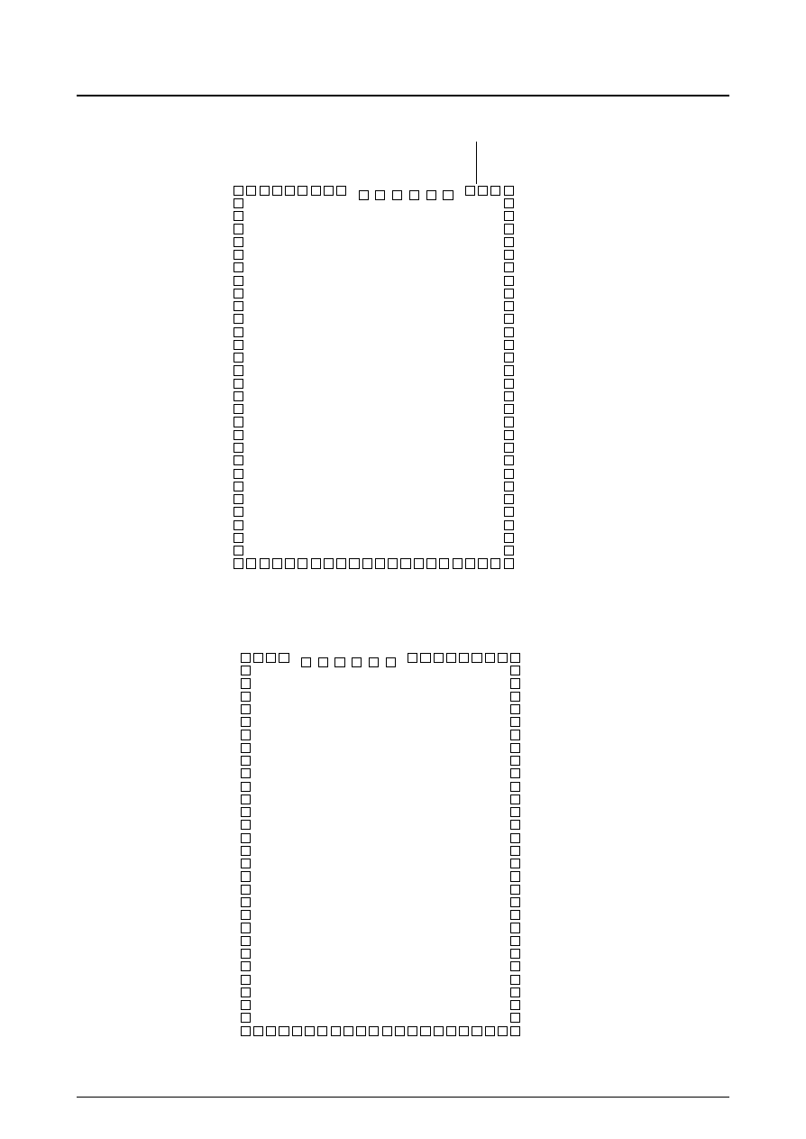
Pad Layout (Top view)
O1
O2
O3
O4
O5
O6
O7
O8
O9
O10
O11
O12
O13
O14
O15
O16
O17
O18
O19
O20
O21
O22
O23
O24
O25
O26
O27
O28
O29
O30
O80
O79
O78
O77
O76
O75
O74
O73
O72
O71
O70
O69
O68
O67
O66
O65
O64
O63
O62
O61
O60
O59
O58
O57
O56
O55
O54
O53
O52
O51
O31
O32
O33
O34
O35
O36
O37
O38
O39
O40
O41
O42
O43
O44
O45
O46
O47
O48
O49
O50
CP
CDI
LO
AD
SDI
DI3
DI2
DI1
M
P/S
DISPOFF
CDO
V1
VDD
V3
V4
VEE
VSS
LC7940YC
O1
O2
O3
O4
O5
O6
O7
O8
O9
O10
O11
O12
O13
O14
O15
O16
O17
O18
O19
O20
O21
O22
O23
O24
O25
O26
O27
O28
O29
O30
O80
O79
O78
O77
O76
O75
O74
O73
O72
O71
O70
O69
O68
O67
O66
O65
O64
O63
O62
O61
O60
O59
O58
O57
O56
O55
O54
O53
O52
O51
O50
O49
O48
O47
O46
O45
O44
O43
O42
O41
O40
O39
O38
O37
O36
O35
O34
O33
O32
O31
CDO
DISPOFF
P/S
M
DI1
DI2
DI3
SDI
LO
AD
CDI
CP
VSS
VEE
V4
V3
VDD
V1
LC7941YC