 | –≠–ª–µ–∫—Ç—Ä–æ–Ω–Ω—ã–π –∫–æ–º–ø–æ–Ω–µ–Ω—Ç: LC7972VA | –°–∫–∞—á–∞—Ç—å:  PDF PDF  ZIP ZIP |

Overview
The LC7972VA and LC7972VB are dual
inverting/noninverting operational amplifier ICs that are
fabricated in a CMOS process. These ICs provide a
programmable offset correction function and a power
saving function for use when the operational amplifier is
unused, both of which can be controlled from a
microprocessor interface.
Features
∑ High input impedance provided by fabrication in a
CMOS process.
∑ Low power provided by fabrication in a CMOS process.
∑ One of two types of operational amplifier can be
selected: inverting (operational amplifier 1) or
noninverting (operational amplifier 2)
∑ Operating supply voltage: 4.9 to 5.2 V
∑ Package: SSOP20
∑ Operating temperature: Ta = ≠30 to +70∞C
∑ The following modes are supported. These are selected
via port level settings.
Package Dimensions
unit: mm
3179A-SSOP20
CMOS LSI
Ordering number : EN5682
73097HA(OT) No. 5682-1/4
SANYO: SSOP20
[LC7972VA, VB]
SANYO Electric Co.,Ltd. Semiconductor Bussiness Headquarters
TOKYO OFFICE Tokyo Bldg., 1-10, 1 Chome, Ueno, Taito-ku, TOKYO, 110 JAPAN
CMOS Operational Amplifier with Programmable
Offset Correction Function
LC7972VA, 7972VB
Port
Level
Function
OP1ON
L
Operational amplifier 1: Operation stopped (low-power mode)
H
Operational amplifier 1: Normal operation (OP2ON must be low in this mode.)
OP2ON
L
Operational amplifier 2: Operation stopped (low-power mode)
H
Operational amplifier 2: Normal operation (OP1ON must be low in this mode.)
OFST1
L
Operational amplifier 1: Offset mode (inverting input = V
SS
)
H
Operational amplifier 1: Operating mode (inverting input = normal input)
OFST2
L
Operational amplifier 2: Offset mode (noninverting input = V
SS
)
H
Operational amplifier 2: Operating mode (noninverting input = normal input)
CLKC
L
Operational amplifier power supply clock: Internal clock
This catalog provides information as of July, 1997. Specifications and information herein are subject to change
without notice.
s
No products described or contained herein are intended for use in surgical implants, life-support systems, aerospace
equipment, nuclear power control systems, vehicles, disaster/crime-prevention equipment and the like, the failure of
which may directly or indirectly cause injury, death or property loss.
s
Anyone purchasing any products described or contained herein for an above-mentioned use shall:
Accept full responsibility and indemnify and defend SANYO ELECTRIC CO., LTD., its affiliates, subsidiaries and
distributors and all their officers and employees, jointly and severally, against any and all claims and litigation and all
damages, cost and expenses associated with such use:
Not impose any responsibility for any fault or negligence which may be cited in any such claim or litigation on
SANYO ELECTRIC CO., LTD., its affiliates, subsidiaries and distributors or any of their officers and employees
jointly or severally.
s
Information (including circuit diagrams and circuit parameters) herein is for example only; it is not guaranteed for
volume production. SANYO believes information herein is accurate and reliable, but no guarantees are made or implied
regarding its use or any infringements of intellectual property rights or other rights of third parties.

Pin Assignment
No. 5682-2/4
LC7972VA, 7972VB
Pin Functions
Pin
Function
No.
Symbol
1
DV
DD
Digital system power supply. Normally connected to +5 V.
2
EXT
Must be tied low.
3
CLKC
Must be tied low.
4
OP2ON
Operational amplifier 2 operation control
5
OFST2
Operational amplifier 2 mode control
6
OP1ON
Operational amplifier 1 operation control
7
OFST1
Operational amplifier 1 mode control
8
TGO
Operational amplifier 1 VSS/small voltage output
9
OP1I
Operational amplifier 1 input
10
OP1O
Operational amplifier 1 output
11
OP2O
Operational amplifier 2 output
12
OP2I
Operational amplifier 2 input
13
TGI
Small voltage input common to operational amplifiers 1 and 2
14
AV
SS
M
Operational amplifier power supply minus voltage generation
15
AV
DD
Analog system power supply. Normally connected to +5 V.
16
AV
SS
P
Operational amplifier power supply external Zener diode connection
17
AV
SS
Analog system ground. Must be connected to 0 V.
18
CUP2
Operational amplifier power supply external capacitor connection 2
19
CUP1
Operational amplifier power supply external capacitor connection 1
20
DV
SS
Digital system ground. Must be connected to 0 V.
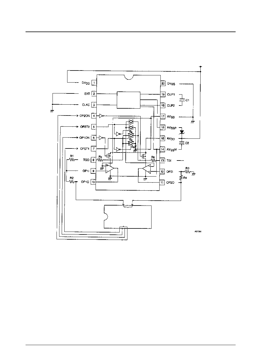
System Block Diagram and Sample Application
A circuit that amplifies very small voltages around the V
SS
level can be constructed by adding the peripheral circuits
shown in the figure below.
No. 5682-3/4
LC7972VA, 7972VB
A/D converter inputs
Port outputs
Microcontroller
Small-voltage input
Step-down
voltage
converter circuit

No. 5682-4/4
LC7972VA, 7972VB
Parameter
Symbol
Conditions
Ratings
Unit
Maximum supply voltage
V
DD
max
V
DD
≠0.3 to +7.0
V
Output voltage
V
O
OP1O, OP2O, TGO
≠0.3 to V
DD
+0.3
V
V
I
1
OP1ON, OFST1, OP2ON, OFST2, EXT, CLKC, CUP2,
≠0.3 to V
DD
+0.3
V
Input voltage
CUP1, AV
SS
P, OP1I, OP2I, TGI
V
I
2
AV
SS
M
≠3 to +0.3
V
Peak output current
I
OP
OP1O, OP2O, TGO
≠1 to +1
mA
Average output current
I
OA
OP1O, OP2O, TGO : The current per pin
≠1 to +1
mA
Allowable power dissipation
Pd max
SSOP20 : Ta = ≠30 to +70∞C
100
mW
Operating temperature
Topr
≠30 to +70
∞C
Storage temperature
Tstg
≠55 to +125
∞C
Specifications
Absolute Maximum Ratings
at Ta = 25∞C, V
SS
= 0 V
Parameter
Symbol
Conditions
Ratings
Unit
min
typ
max
Supply voltage
V
DD
V
DD
4.9
5.2
V
Input high-level voltage
V
IH
OP1ON, OFST1, OP2ON, OFST2
0.7 V
DD
V
DD
V
Input low-level voltage
V
IL
1
OP1ON, OFST1, OP2ON, OFST2, CLKC
V
SS
0.3 V
DD
V
V
IL
2
EXT
V
SS
0.3 V
DD
V
Common-mode input voltage
V
IC
0
4.2
V
Voltage drop
D
V
AV
SS
M: Zener diode = 5.1 V (X rank specified)
≠0.2
V
Allowable Operating Ranges
at Ta = ≠30 to +70∞C, V
SS
= 0 V, V
DD
= 4.9 to 5.2 V, unless otherwise specified
Parameter
Symbol
Conditions
Ratings
Unit
min
typ
max
Input high-level current
I
IH
1
OP1ON, OFST1, OP2ON, OFST2 : V
IN
= V
DD
1.0
µA
I
IH
2
TGI: V
IN
= V
DD
, with the built-in TG off.
1.0
µA
I
IL
1
OP1ON, OFST1, OP2ON, OFST2, EXT,
≠1.0
µA
Input low-level current
CLKC : V
IN
= V
SS
I
IL
2
TGI: V
IN
= V
SS
, with the built-in TG off.
≠1.0
µA
Output high-level voltage
V
OH
OP1O, OP2O : I
OH
= ≠3 µA
V
DD
≠ 0.5
V
Output low-level voltage
V
OL
OP1O, OP2O : I
OL
= 3 µA
0.5
V
Operational amplifier 1 gain-related resistance
Rtg + 2Rs TGO, TGI
500
700
900
Operational amplifier 1 gain-related resistance
|Rx≠Ry|
TGO, TGI: Offset mode: Rx = Rtg + 2Rs
80
difference
Operating mode: Ry = Rtg + 2Rs
Current drain
Operating
I
DDOP
V
DD
; Using the internal clock, with the
700
900
µA
operational amplifier 1 circuit operating.
Standby
I
DDST
V
DD
; Both operational amplifiers 1 and 2
0.05
10
µA
stopped.
Electrical Characteristics
at Ta = ≠30 to +70∞C, V
SS
= 0 V, V
DD
= 4.9 to 5.2 V, unless otherwise specified
Parameter
Symbol
Conditions
Ratings
Unit
min
typ
max
Input offset voltage
V
IO
OP1I, OP2I : LC7972VA
5
10.5
mV
LC7972VB
5
15
mV
Supply voltage rejection ratio
P
SRR
1 kHz
60
dB
Common-mode rejection ratio
C
MRR
60
dB
Open-loop voltage gain
A
O
80
dB
0-dB bandwidth
f
T
90
kHz
Maximum output voltage
V
O
OP1O, OP2O : R
L
100 k
V
DD
≠ 0.5
V
Current drain
I
CC
For the operational amplifier 1 circuit
100
µA
Settling time
T
SET
OP1O, OP2O
900
µs
Operational Amplifier Characteristics
at Ta = 25∞C ±2∞C, V
SS
= 0 V, V
DD
= 4.9 to 5.2 V, unless otherwise specified