 | –≠–ª–µ–∫—Ç—Ä–æ–Ω–Ω—ã–π –∫–æ–º–ø–æ–Ω–µ–Ω—Ç: LC89512W | –°–∫–∞—á–∞—Ç—å:  PDF PDF  ZIP ZIP |

Ordering number : EN
*
4852B
O3095HA (OT)/D1694TH (OT) No. 4852-1/5
Overview
The LC89512W integrates a real-time error correction
circuit and a SCSI interface in a single chip.
Functions
∑ CD-ROM error correction function, subcode readout
function, SCSI interface
Features
∑ Support for double-speed drives at an operating
frequency of 16.9344 MHz
Either SRAM (120 ns), DRAM (80 ns) or pseudo
SRAM (85 ns) can be used.
∑ Support for quad-speed drives at an operating frequency
of 33.8688 MHz
SRAM (70 ns) must be used.
∑ Built-in SCSI interface with built-in 48 mA sink buffer
(Only the TARGET function is supported.)
∑ Built-in 12-byte output FIFO for sub-CPU to host
computer data transmission
∑ Built-in 12-byte input FIFO for host computer to sub-
CPU data transmission
∑ Subcode data can be written to buffer RAM and the sub-
CPU can read the subcode values by connecting the
LC89512 to the CD-DSP subcode pin.
∑ Sub-CPU access of buffer RAM through the LC89512
∑ Built-in function for buffer RAM internal data transfer
∑ Pseudo-SRAM (128-kword
◊
8-bit and smaller) can be
used.
∑ DRAM (two 256-kword
◊
4-bit chips or two 1-Mword
◊
4-bit chips) can be used.
∑ Transfer speeds:
2.8 MB/second (asynchronous mode) (for CD-ROM
decode only operation)
4.2 MB/second (synchronous mode) (CD-ROM decode
operation is not supported in synchronous mode)
Both of these transfer modes use a 16.9344 MHz clock.
(The transfer speed depends on the frequency used.)
∑ Operating frequencies: 16.9344 MHz (up to double
speed), 33.8688 (quad speed)
Package Dimensions
unit: mm
3181A-SQFP100
Preliminary
SANYO: SQFP100
[LC89512W]
LC89512W
SANYO Electric Co.,Ltd. Semiconductor Bussiness Headquarters
TOKYO OFFICE Tokyo Bldg., 1-10, 1 Chome, Ueno, Taito-ku, TOKYO, 110-8534 JAPAN
CD-ROM Error Correction LSI
with Built-In SCSI Interface
CMOS LSI

Block Diagram
No. 4852-2/5
LC89512W
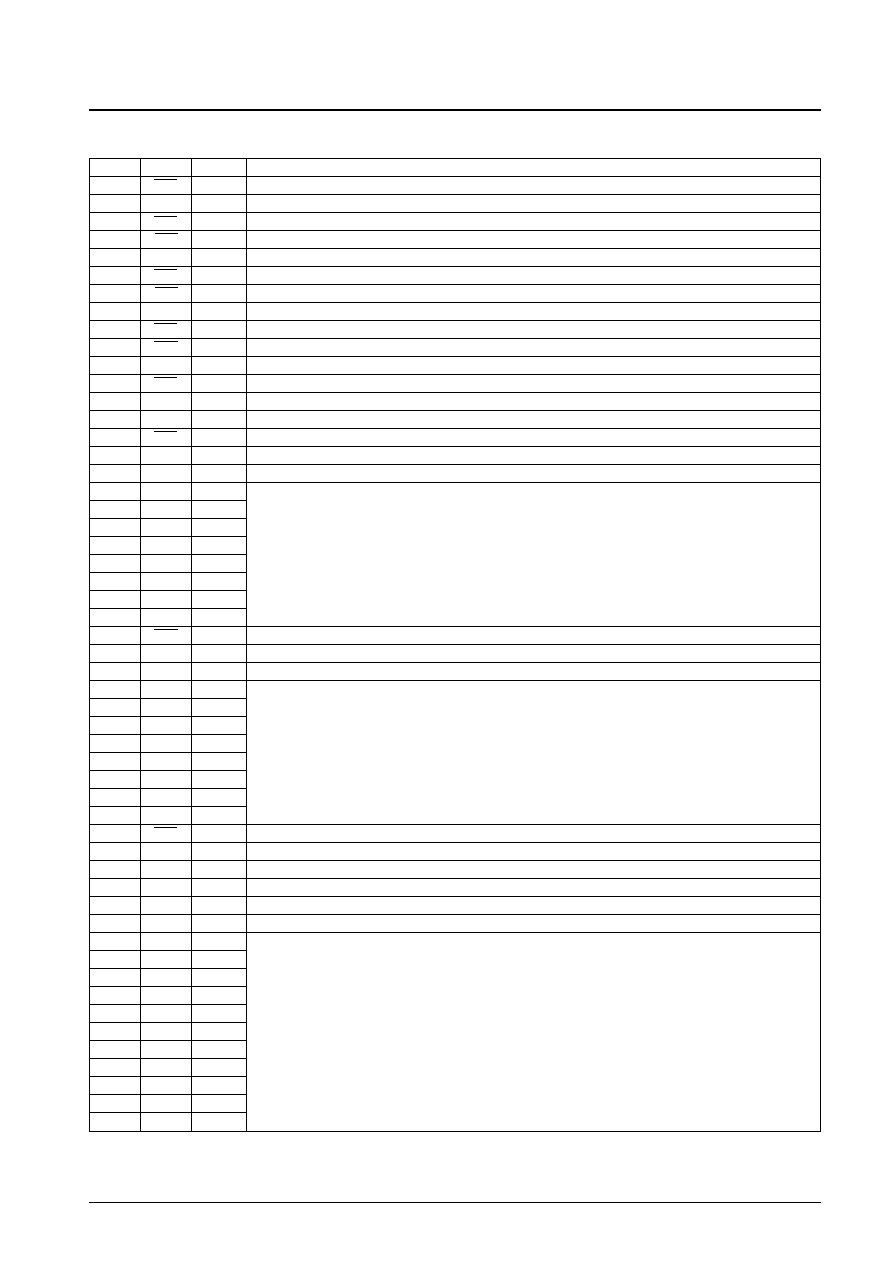
Pin Functions
Type: I: Input pin, O: Output pin, B: Bidirectional pin, P: Power supply pin, NC: No connection pin
No. 4852-3/5
LC89512W
Continued on next page.
Pin No.
Pin
Type
Function
1
DB7
B
SCSI connection
2
V
SS
1
P
3
DBP
B
SCSI connection
4
ATN
B
SCSI connection
5
V
SS
1
P
6
BSY
B
SCSI connection
7
ACK
B
SCSI connection
8
V
SS
1
P
9
RST
B
SCSI connection
10
MSG
B
SCSI connection
11
V
SS
1
P
12
SEL
B
SCSI connection
13
C/D
B
SCSI connection
14
V
SS
1
P
15
REQ
B
SCSI connection
16
I/O
B
SCSI connection
17
V
SS
0
P
18
I
O
0
B
19
I
O
1
B
20
I
O
2
B
21
I
O
3
B
Data buffer RAM data signals
22
I
O
4
B
These pins have built-in pull-up resistors.
23
I
O
5
B
24
I
O
6
B
25
I
O
7
B
26
INT1
O
SCSI block interrupt request signal output (set using a register)
27
V
SS
0
P
28
V
SS
0
P
29
D0
B
30
D1
B
31
D2
B
32
D3
B
Microprocessor data signals
33
D4
B
These pins have built-in pull-up resistors.
34
D5
B
35
D6
B
36
D7
B
37
INT0
O
Microprocessor interrupt request signal output
38
XTALCK
I
Crystal oscillator circuit input
39
XTAL
O
Crystal oscillator circuit output
40
V
SS
0
P
41
V
DD
P
42
RA0
O
43
RA1
O
44
RA2
O
45
RA3
O
46
RA4
O
47
RA5
O
48
RA6
O
Data buffer RAM address signal outputs
49
RA7
O
50
RA8
O
51
RA9
O
52
RA10
O
53
RA11
O
Continued from preceding page.
Type: I: Input pin, O: Output pin, B: Bidirectional pin, P: Power supply pin, NC: No connection pin
Note: 1. NC must be left open. Do not connect any signals to these pins.
2. V
SS
0 is the logic system ground and V
SS
1 is the SCSI interface ground. (from the standard cell version)
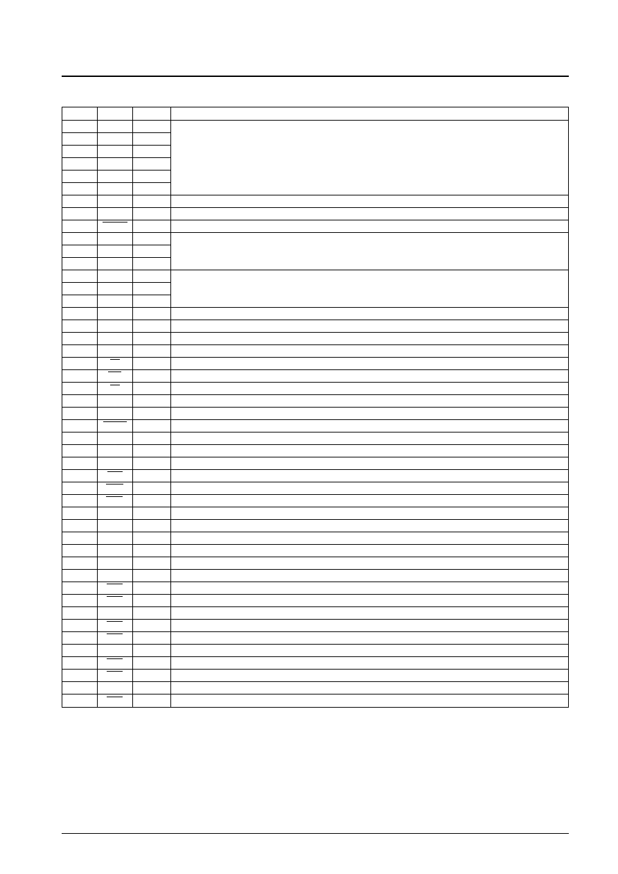
No. 4852-4/5
LC89512W
Pin No.
Pin
Type
Function
54
RA12
O
55
RA13
O
56
RA14
O
Data buffer RAM address signal outputs
57
RA15
O
58
RA16
O
59
RA17
O
60
V
DD
P
61
V
SS
0
P
62
RESET
I
Reset
63
TEST1
I
64
TEST2
I
Test inputs. These pins should be tied low in normal operation.
65
TEST3
I
66
WFCK
I
67
SBSO
I
Subcode I/O
68
SCOR
I
69
SDATA
I
Serial data input
70
BCK
I
Serial data input clock
71
LRCK
I
44.1 kHz strobe signal input
72
C2PO
I
C2 pointer input
73
RD
I
Microprocessor data read signal input
74
WR
I
Microprocessor data write signal input
75
CS
I
Chip select signal input (from the microprocessor)
76
RS
I
Register selection signal input
77
V
SS
0
P
78
SWAIT
O
Sub-CPU wait signal
79
EXCK
O
Sub code I/O
80
MCK
O
Crystal oscillator frequency output
81
TEST0
I
Test inputs. These pins should be tied low in normal operation
.
82
RCS
O
RAM chip select
83
RWE
O
RAM data write signal output
84
ROE
O
RAM data read signal output
85
NC
86
NC
87
NC
88
NC
89
V
DD
P
90
V
SS
1
P
91
DB0
B
SCSI connection
92
DB1
B
SCSI connection
93
V
SS
1
P
94
DB2
B
SCSI connection
95
DB3
B
SCSI connection
96
V
SS
1
P
97
DB4
B
SCSI connection
98
DB5
B
SCSI connection
99
V
SS
1
P
100
DB6
B
SCSI connection
Continued on next page.

No. 4852-5/5
LC89512W
Specifications
Absolute Maximum Ratings
at V
SS
= 0 V
Allowable Operating Ranges
at Ta = ≠30 to +70∞C, V
SS
= 0 V
DC Characteristics
at Ta = ≠30 to +70∞C, V
SS
= 0 V, V
DD
= 4.5 to 5.5 V
This catalog provides information as of February, 1997. Specifications and information herein are subject to
change without notice.
s
No products described or contained herein are intended for use in surgical implants, life-support systems, aerospace
equipment, nuclear power control systems, vehicles, disaster/crime-prevention equipment and the like, the failure of
which may directly or indirectly cause injury, death or property loss.
s
Anyone purchasing any products described or contained herein for an above-mentioned use shall:
Accept full responsibility and indemnify and defend SANYO ELECTRIC CO., LTD., its affiliates, subsidiaries and
distributors and all their officers and employees, jointly and severally, against any and all claims and litigation and all
damages, cost and expenses associated with such use:
Not impose any responsibility for any fault or negligence which may be cited in any such claim or litigation on
SANYO ELECTRIC CO., LTD., its affiliates, subsidiaries and distributors or any of their officers and employees
jointly or severally.
s
Information (including circuit diagrams and circuit parameters) herein is for example only; it is not guaranteed for
volume production. SANYO believes information herein is accurate and reliable, but no guarantees are made or implied
regarding its use or any infringements of intellectual property rights or other rights of third parties.
Parameter
Symbol
Conditions
Ratings
Unit
Maximum supply voltage
V
DD
max
Ta = 25∞C
≠0.3 to +7.0
V
I/O voltages
V
I
V
O
Ta = 25∞C
≠0.3 to V
DD
+ 0.3
V
Allowable power dissipation
Pd max
Ta
70∞C
350
mW
Operating temperature
Topr
≠30 to +70
∞C
Storage temperature
Tstg
≠55 to +125
∞C
Soldering thermal stress limit (pins only)
10 seconds
260
∞C
Parameter
Symbol
Conditions
min
typ
max
Unit
Supply voltage
V
DD
4.5
5.0
5.5
V
Input voltage range
V
IN
0
V
DD
V
Parameter
Symbol
Conditions
min
typ
max
Unit
Input high level voltage
V
IH
1
All input pins other than (1), (3), and XTALCK
2.2
V
Input low level voltage
V
IL
1
0.8
V
Input high level voltage
V
IH
2
RESET, I
O
0 to I
O
7, D0 to D7, RD, CS, WR, WFCK,
2.5
V
Input low level voltage
V
IL
2
SBSO and SCOR(1)
0.6
V
Input high level voltage
V
IH
3
ACK, ATN and the input pins (3)
2.0
V
Input low level voltage
V
IL
3
0.8
V
Output high level voltage
V
OH
1
I
OH
1 = ≠3 mA: I
O
0 to I
O
7, D0 to D7 and all output pins
2.4
V
other than (2), (3) and XTALCK
Output low level voltage
V
OL
1
I
OL
1 = 3 mA: I
O
0 to I
O
7, D0 to D7 and all output pins
0.4
V
other than (2), (3) and XTALCK
Output low level voltage
V
OL
2
I
OL
2 = 3 mA: INT1 and INT0
0.4
V
(pull-up resistor open drain) (2)
Output low level voltage
V
OL
3
I
OL
3 = 48 mA: DB0 to DB7, DBP, BSY, I/O, MSG, SEL,
0.4
V
RST, REQ, C/D (2)
Input leakage current
I
L
V
I
= V
SS
, V
DD
: All input pins
≠25
+25
µA
Pull-up resistance
R
UP
I
O
0 to I
O
7, D0 to D7, INT1 and INT0
40
80
160
k