 | –≠–ª–µ–∫—Ç—Ä–æ–Ω–Ω—ã–π –∫–æ–º–ø–æ–Ω–µ–Ω—Ç: LC89513KP | –°–∫–∞—á–∞—Ç—å:  PDF PDF  ZIP ZIP |
Ordering number : EN
*
4853A
D1694TH (OT) No. 4853-1/5
Overview
The LC89513K is an error correction LSI appropriate for
systems in which a single CPU handles both system
control and data readout. The LC89513K consists of the
three major blocks described below.
∑ CD Player Interface/Data Input Block
The LC89513K supports three serial input formats, with
the format used selected by setting internal register. That
is, an application system can compensate for CD player
serial data format differences by setting the LC89513K
CDIF0 and CDIF1 registers.
The LC89513K uses an internal synchronization
detection circuit to synchronize internal operations with
the input data in block (sector) units. LC89513K
synchronization uses not only input data pattern
detection, but also uses a synchronization signal
interpolation circuit for synchronization protection.
These two synchronization systems can be turned on and
off under program control. Input data is stored in buffer
RAM in 8-bit units after being processed by a
descrambling circuit. All of the 2,352 bytes of the input
data, including the synchronization, header and parity
data, is stored in RAM in the order received from the
CD player without exception.
∑ Error Correction Block
This block corrects the errors in the CD-ROM data
output from the CD player block.
CD-ROM data output from the CD player is temporarily
stored in the LC89513K's external buffer RAM. After
one sector is buffered, the LC89513K automatically
performs error correction. (Error detection and
correction are only performed once.) After the
correction procedure completes, the LC89513K issues
an interrupt to the control CPU, and the control CPU
reads the data through the LC89513K.
Since the buffering, error correction, and data read
operations are pipelined, as they are in the LC8951,
these operations are performed in real time.
∑ CPU Interface Block
In the LC8951, the CPU interface was divided into a
microcontroller interface block (the LC8951 control
bus) and a host interface block (data output bus).
However, in the LC89513K, these functions are
combined in a single block so that a single CPU can both
control the CD player and read data from the LC89513K.
The LC89513K outputs CD-ROM data from a separate
port (pin), as did the earlier LC8951. The LC89513K
CPU interface uses the same indirect addressing scheme
used in the LC8951 interface, and programs written for
the LC8951 can be used without modification.
Features
∑ Supports both double- and quad-speed playback,
selectable by internal register settings.
Operating frequencies: double-speed: 16.9344 MHz,
quad speed: 33.8688 MHz
∑ Can be operated at 3.5 V.
In normal operation SRAM with an access time of
300 ns or shorter must be used.
In double-speed operation SRAM with an access time of
120 ns or shorter must be used.
∑ Supports CD-ROM drive systems in which a single CPU
performs both control and data readout functions.
Preliminary
LC89513K
SANYO Electric Co.,Ltd. Semiconductor Bussiness Headquarters
TOKYO OFFICE Tokyo Bldg., 1-10, 1 Chome, Ueno, Taito-ku, TOKYO, 110-8534 JAPAN
CD-ROM/CD-I Error Correction LSI
for Integrated Host CPU Systems
CMOS LSI
Any and all SANYO products described or contained herein do not have specifications that can handle
applications that require extremely high levels of reliability, such as life-support systems, aircraft's
control systems, or other applications whose failure can be reasonably expected to result in serious
physical and/or material damage. Consult with your SANYO representative nearest you before using
any SANYO products described or contained herein in such applications.
SANYO assumes no responsibility for equipment failures that result from using products at values that
exceed, even momentarily, rated values (such as maximum ratings, operating condition ranges, or other
parameters) listed in products specifications of any and all SANYO products described or contained
herein.
Specifications
Absolute Maximum Ratings
at V
SS
= 0 V
Allowable Operating Ranges
at Ta = ≠30 to +70∞C, V
SS
= 0 V
DC Characteristics
at Ta = ≠30 to +70∞C, V
SS
= 0 V, V
DD
= 3.5 to 5.5 V
No. 4853-2/5
LC89513K
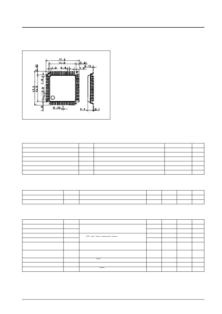
Package Dimensions
unit: mm
3159-QFP64E
SANYO: QFP64E
[LC89513K]
Parameter
Symbol
Conditions
Ratings
Unit
Maximum supply voltage
V
DD
max
Ta = 25∞C
≠0.3 to +7.0
V
I/O voltages
V
I
V
O
Ta = 25∞C
≠0.3 to V
DD
+ 0.3
V
Allowable power dissipation
Pd max
Ta
70∞C
350
mW
Operating temperature
Topr
≠30 to +70
∞C
Storage temperature
Tstg
≠55 to +125
∞C
Soldering thermal stress limit
10 seconds
260
∞C
Parameter
Symbol
Conditions
min
typ
max
Unit
Supply voltage
V
DD
3.5
5.0
5.5
V
Input voltage range
V
IN
0
V
DD
V
Parameter
Symbol
Conditions
min
typ
max
Unit
Input high level voltage
V
IH
1
All input pins other than (1) and XTALCK
2.2
V
Input low level voltage
V
IL
1
0.8
V
Input high level voltage
V
IH
2
RS, CS, RD, WR, RESET, HRD and I
O
0 to I
O
7 (1)
2.5
V
Input low level voltage
V
IL
2
0.6
V
Output high level voltage
V
OH
1
I
OH
1 = ≠3 mA: All output pins (including bus pins)
2.4
V
other than (2) and XTALCK
Output low level voltage
V
OL
1
I
OL
1 = 3 mA: All output pins (including bus pins)
0.4
V
other than (2) and XTALCK
Output low level voltage
V
OL
2
I
OL
2 = 3 mA: INT (pull-up resistor open drain) (2)
0.4
V
Input leakage current
I
L
V
I
= V
SS
, V
DD
: All input pins
≠25
+25
µA
Pull-up resistance
R
UP
All bus pins and INT
10
20
40
k

Block Diagram
No. 4853-3/5
LC89513K

Pin Functions
Type: I: Input pin, O: Output pin, B: Bidirectional pin, P: Power supply pin, NC: No connection pin
No. 4853-4/5
LC89513K
Continued on next page.
Pin No.
Pin
Type
Function
1
V
SS
P
2
RA0
O
3
RA1
O
4
RA2
O
5
RA3
O
Data buffer RAM address signal outputs
6
RA4
O
7
RA5
O
8
RA6
O
9
V
SS
P
10
RA7
O
11
RA8
O
12
RA9
O
13
RA10
O
Data buffer RAM data signals
14
RA11
O
15
RA12
O
16
RA13
O
17
V
SS
P
18
RA13B
O
Data buffer RAM address signal output
19
RCS
O
RAM chip select
20
RWE
O
RAM data write signal output
21
ROE
O
RAM data write signal output
22
RESET
I
Chip select signal input
23
XTALCK
I
Crystal oscillator circuit input
24
V
DD
P
25
C2PO
I
C2 pointer input
26
BCK
I
Serial data input clock
27
SDATA
I
Serial data input
28
LRCK
I
44.1 kHz strobe signal input
29
RS
I
Register selection signal input
30
RD
I
CPU data read signal input
31
WR
I
CPU data write signal input
32
CS
I
Chip select signal input (from the CPU)
33
V
SS
P
34
D0
B
35
D1
B
36
D2
B
37
D3
B
CPU data signal pins
38
D4
B
These pins have built-in pull-up resistors.
39
D5
B
40
D6
B
41
D7
B
42
GSRAM
I
Pseudo-SRAM selection
43
INT
O
CPU interrupt request signal output
44
DRQ
O
DRQ signal output
45
HD0
O
46
HD1
O
Data outputs to the CPU
47
HD2
O
48
HD3
O
49
V
SS
P
50
HD4
O
51
HD5
O
Data outputs to the CPU
52
HD6
O
53
HD7
O
No. 4853-5/5
LC89513K
Continued from preceding page.
Type: I: Input pin, O: Output pin, B: Bidirectional pin, P: Power supply pin, NC: No connection pin
This catalog provides information as of August, 1998. Specifications and information herein are subject to
change without notice.
Specifications of any and all SANYO products described or contained herein stipulate the performance,
characteristics, and functions of the described products in the independent state, and are not guarantees
of the performance, characteristics, and functions of the described products as mounted in the customer's
products or equipment. To verify symptoms and states that cannot be evaluated in an independent device,
the customer should always evaluate and test devices mounted in the customer's products or equipment.
SANYO Electric Co., Ltd. strives to supply high-quality high-reliability products. However, any and all
semiconductor products fail with some probability. It is possible that these probabilistic failures could
give rise to accidents or events that could endanger human lives, that could give rise to smoke or fire,
or that could cause damage to other property. When designing equipment, adopt safety measures so
that these kinds of accidents or events cannot occur. Such measures include but are not limited to protective
circuits and error prevention circuits for safe design, redundant design, and structural design.
In the event that any and all SANYO products described or contained herein fall under strategic
products (including services) controlled under the Foreign Exchange and Foreign Trade Control Law of
Japan, such products must not be exported without obtaining export license from the Ministry of
International Trade and Industry in accordance with the above law.
No part of this publication may be reproduced or transmitted in any form or by any means, electronic or
mechanical, including photocopying and recording, or any information storage or retrieval system,
or otherwise, without the prior written permission of SANYO Electric Co., Ltd.
Any and all information described or contained herein are subject to change without notice due to
product/technology improvement, etc. When designing equipment, refer to the "Delivery Specification"
for the SANYO product that you intend to use.
Information (including circuit diagrams and circuit parameters) herein is for example only; it is not
guaranteed for volume production. SANYO believes information herein is accurate and reliable, but
no guarantees are made or implied regarding its use or any infringements of intellectual property rights
or other rights of third parties.
Pin No.
Pin
Type
Function
54
HRD
I
Data read signal input
55
DTEN
O
Data enable signal output
56
V
DD
P
57
I
O
0
B
58
I
O
1
B
59
I
O
2
B
60
I
O
3
B
Data buffer RAM data signals
61
I
O
4
B
These pins have built-in pull-up resistors.
62
I
O
5
B
63
I
O
6
B
64
I
O
7
B