 | –≠–ª–µ–∫—Ç—Ä–æ–Ω–Ω—ã–π –∫–æ–º–ø–æ–Ω–µ–Ω—Ç: LC895196 | –°–∫–∞—á–∞—Ç—å:  PDF PDF  ZIP ZIP |
Overview
The LC895196 is a large scale integrated circuit equipped
with CD-ROM functions and an internal ATA-PI (IDE)
interface.
Functions
∑ CD-ROM ECC functions, SUB-CODE read function,
ATA-PI (IDE) interface (Registers, etc.), and a CAV-
audio function.
Features
∑ Built-in ATA-PI (IDE) interface.
∑ 24
◊
speed supported
Uses the EDO-DRAM (
◊
16, 60 ns)
16.6 Mbyte/s (with IORDY)
Operating frequency: 27.5 MHz
∑ 20
◊
speed supported
Uses the EDO-DRAM (
◊
16, 60 ns)
16.6 Mbyte/s (without IORDY)
Operating frequency: 27 MHz
∑ 12
◊
speed supported
Uses DRAM (
◊
16, 70 ns)
∑ Supports between 1 Mbit and 32 Mbit of buffer RAM
when DRAM is used
∑ The user can flexibly set the CD main channel, the C2
flags, and the subcode regions in the buffer RAM
∑ Built-in batch transfer function. (Where the batch
transfer function is a function that transmit the CD main
channel, C2 flags, subcodes, etc. all at once.)
∑ Built-in multitransmit function. (Where the
multitransmit function is a function that automatically
transmits multiple blocks at once.)
∑ Built-in CAV-audio functions
∑ Built-in intelligent functions (auto buffering, auto
decoding, CD-R compatibility)
∑ Built in subcode P-W buffering function (NO-ECC) and
CD-TEXT compatibility
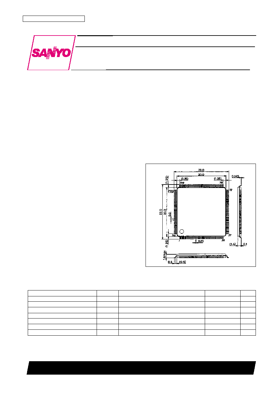
Package Dimensions
unit: mm
3214-SQFP144
CMOS LSI
Ordering number : EN
*
5737A
D3097HA (OT) No. 5737-1/12
Preliminary
SANYO Electric Co.,Ltd. Semiconductor Bussiness Headquarters
TOKYO OFFICE Tokyo Bldg., 1-10, 1 Chome, Ueno, Taito-ku, TOKYO, 110 JAPAN
ATA-PI Compatible CD-ROM Decoder IC
LC895196
Specifications
Absolute Maximum Ratings
at V
SS
= 0 V
Parameter
Symbol
Condition
Ratings
Unit
Maximum supply voltage
V
DD
max
Ta = 25∞C
≠0.3 to +7.0
V
I/O voltage
V
I
, V
O
max
Ta = 25∞C
≠0.3 to V
DD
+ 0.3
V
Allowable power dissipation
Pd max
Ta
70∞C
550
mW
Operating temperatures
Topr
≠30 to +70
∞C
Storage temperatures
Tstg
≠55 to +125
∞C
Soldering temperature (terminals only)
For 10 seconds
235
∞C
I/O current
I
I
, I
O
max
±20
*
mA
[LC895196]
SANYO: SQFP144
Note:
*
Per basic I/O cell
Allowable Operating Ranges
at Ta = ≠30 to +70∞C, V
SS
= 0 V
DC Characteristics
at V
SS
= 0 V, V
DD
= 4.5 to 5.5 V, Ta = ≠30 to +70∞C
Note: The applicable pins correspond to the following names.
[INPUT]
(1) ..........ATPINSEL, CSCTRL, SUA0 to SUA6, BCK, C2PO, LRCK, SDATA, SBSO, SCOR, WFCK, TEST0, TEST1
(2) ..........ZRESET, ZCS, ZRD, ZWR, CSEL
(3) ..........DA0 to DA2, ZCS1FX, ZCS3FX, ZDIOR, ZDIOW, ZDMACK, ZHRST
[OUTPUT]
(4) ..........RA0 to RA9, ZCAS0, ZCAS1, ZLWE, ZOE, ZRAS0, ZRAS1, ZUWE, DBCK, DLRCK, DSDATA, EXCK
(5) ..........MCK, MCK2, MCK3
(6) ..........ZRSTCPU, ZRSTIC
(7) ..........ZINT, ZINT1, ZSWAIT
(8) ..........DMARQ, HINTRQ
(9) ..........IORDY, ZIOCS16
[INPUT]
(10) ..........D0 to D7, IO0 to IO15
(11) ..........DD0 to DD15, ZDASP, ZPDIAG
*
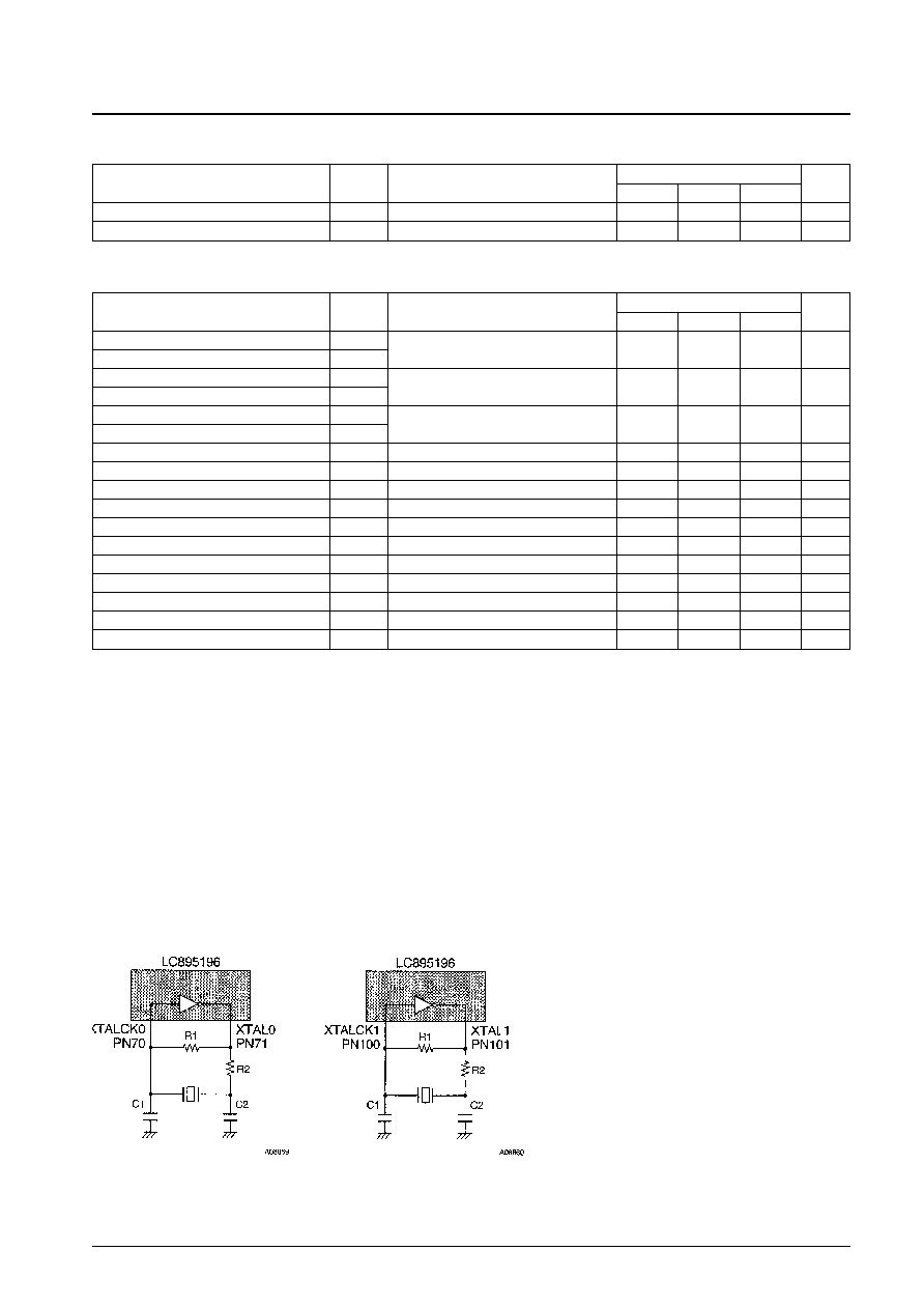
The XTAL0, XTALCK0, XTAL1, XTALCK1 pins are not included in the CD characteristics.
Recommended Example of Oscillator Circuit
No. 5737-2/12
LC895196
Parameter
Symbol
Conditions
Ratings
Unit
min
typ
max
Supply voltage
V
DD
4.5
5.0
5.5
V
Input voltage range
V
IN
0
V
DD
V
Parameter
Symbol
Conditions
Ratings
Unit
Applicable pins (see below)
min
typ
max
Input high level voltage
V
IH
1
TTL compatible (1)
2.2
V
Input low level input
V
IL
1
0.8
V
Input high level voltage
V
IH
2
TTL compatible with pull-up resistor: (10)
2.2
V
Input low level input
V
IL
2
0.8
V
Input high level voltage
V
IH
3
TTL compatible Schmitt: (2), (3), (11)
2.4
V
Input low level input
V
IL
3
0.8
V
Output high level voltage
V
OH
1
I
OH
= ≠2 mA: (4), (10)
V
DD
≠ 2.1
V
Output low level voltage
V
OL
1
I
OL
= 2 mA: (4), (10)
0.4
V
Output high level voltage
V
OH
2
I
OH
= ≠8 mA: (5)
V
DD
≠ 2.1
V
Output: Low level voltage
V
OL
2
I
OL
= 8 mA: (5)
0.4
V
Output high level voltage
V
OH
3
I
OH
= ≠4 mA: (8), (11)
V
DD
≠ 2.1
V
Output low level voltage
V
OL
3
I
OL
= 24 mA: (8), (11)
0.4
V
Output low level voltage
V
OL
4
I
OL
= 2 mA: (9)
0.4
V
Output low level voltage
V
OL
5
I
OL
= 8 mA: (6), (7)
0.4
V
Input leakage current
I
IL
V
I
= V
SS
, V
DD
: (1), (2), (3), (11)
≠10
+10
µA
Output leakage current
I
OZ
When high impedance output: (6), (8), (9), (11)
≠10
+10
µA
Pull-up resistor
R
UP
(7), (10)
40
80
160
k
R1 = 1 M
R2 = 47
C1 = 0
C2 = 47 pF
Ceramic oscillator frequency = 33.8688 MHz.
The 33.8688 MHz recommended example is for a 3
◊
overtone.
R1 = 1 M
R2 = 15
C1 = 0
C2 = 15 pF
Ceramic oscillator frequency (XTALCK0) = 50 MHz
Because the specific values are influenced by the circuit board,
confer with the oscillator manufacturer.
No. 5737-3/12
LC895196
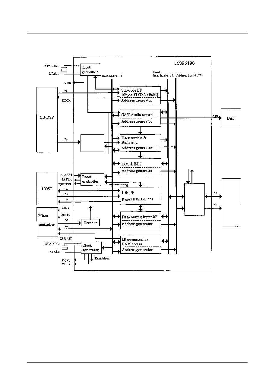
Block Diagram
*
1
WFCK, SBSO, SCOR
*
2
BCK, SDATA, LRCK, C2PO
*
3
DD0 to DD15, ZDASP, ZPDIAG
*
4
ZCS1FX, ZCS3FX, DA0 to DA2, ZDIOR, ZDIOW, ZDMACK, CSEL
*
5
DMARQ, HINTRQ, ZIOCS16, IORDY, ZHRST
*
6
ZRD, ZWR, SUA0 to SUA6, ZCS, CSCTRL
*
7
D0 to D7
*
8
IO0 to IO15
*
9
RA0 to RA9, ZRAS0, ZRAS1, ZCAS0, ZCAS1, ZOE, ZUWE, ZLWE
*
10
DBCK, DLRCK, DSDATA
**
1
HISIDE (WD25C32) is made by WESTERN DIGITAL
External
buffer
DRAM
Bus
arbiter
&
DRAM
controller
Each
block bus
control
signal
CD-DSP I/F
& SYNC
detector
Each block
register
R0 to R118
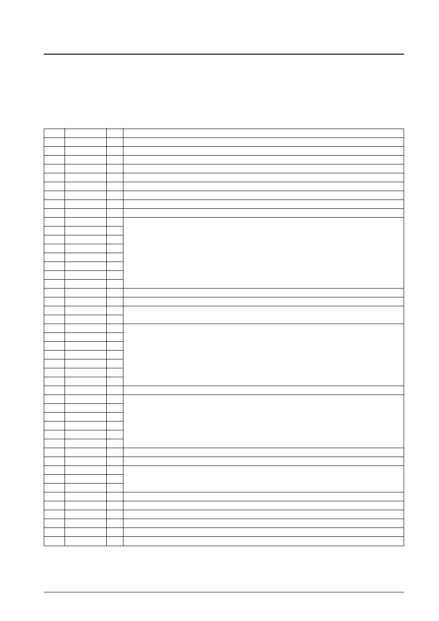
Pin Functions
The LC895196 can be set to the opposite of the ATAPI pin layout using the setting of pin 29.
Pin 29 ATPINSEL = 0
No. 5737-4/12
LC895196
Pin No.
Symbol
Type
Function
1
V
SS0
P
2
ZRAS0
O
RAS signal output pin 0 to the buffer DRAM (Normally uses 0).
3
ZRAS1
O
RAS signal output pin 1 to the buffer DRAM
4
ZCAS0
O
CAS signal output pin 0 to the buffer DRAM (Normally uses 0).
5
ZCAS1
O
CAS signal output pin 1 to the buffer DRAM
6
ZOE
O
Buffer DRAM output enable
7
ZUWE
O
Buffer DRAM upper write enable
8
ZLWE
O
Buffer DRAM lower write enable
9
V
SS0
P
10
RA0
O
11
RA1
O
12
RA2
O
13
RA3
O
Address signal output pins to the data buffer DRAM
14
RA4
O
15
RA5
O
16
RA6
O
17
RA7
O
18
V
DD
P
19
V
SS0
P
20
RA8
O
Address signal output pins to the data buffer DRAM
21
RA9
O
22
IO0
B
23
IO1
B
24
IO2
B
Data I/O pin to the data buffer DRAM.
25
IO3
B
Built-in pull-up resistor.
26
IO4
B
27
IO5
B
28
IO6
B
29
ATPINSEL
I
ATAPI pin assignment select pin. Connect to V
SS0
.
30
IO7
B
31
IO8
B
32
IO9
B
Data I/O pin to the data buffer DRAM.
33
IO10
B
Built-in pull-up resistor.
34
IO11
B
35
IO12
B
36
V
SS0
P
37
V
DD
P
38
IO13
B
Data I/O pin to the data buffer DRAM.
39
IO14
B
40
IO15
B
Built-in pull-up resistor.
41
NC
42
V
SS0
P
43
V
SS0
P
44
V
SS0
P
45
NC
46
NC
Continued on next page.
I: Input pin B: Bi-directional pin NC: Not connected O: Output pin P: Power supply pin
No. 5737-5/12
LC895196
Pin No.
Symbol
Type
Function
47
C2PO
I
48
SDATA
I
CD-DSP interface
49
BCK
I
50
LRCK
I
51
EXCK
O
52
WFCK
I
Subcode I/O
53
SBSO
I
54
V
DD
P
55
V
SS0
P
56
SCOR
I
Subcode I/O
57
DSDATA
O
58
DLRCK
O
DAC output
59
DBCK
O
60
MCK
O
XTALCK1 1/1, 1/2 and STOP output
61
TEST0
I
Test input pin. Connect to V
SS
.
62
TEST1
I
63
CSEL
I
ATAPI control signal
64
ZRSTIC
O
Reset signal to the drive reset IC
65
CSCTRL
I
Microcontroller-side CS active low/high select pin
66
MCK2
O
XTALCK0 1/1, 1/2, 1/5, 1/512 and STOP output
67
MCK3
O
XTALCK0 1/1, 1/5, 2/5, 1/512 and STOP output
68
V
SS0
P
69
NC
70
XTALCK0
I
X'tal oscillator circuit input
71
XTAL0
O
X'tal oscillator circuit input
72
V
SS0
P
73
V
DD
P
74
ZRESET
I
LSI reset
75
ZRD
I
Microcontroller data read signal input
76
ZWR
I
Microcontroller data write signal input
77
ZCS
I
Input pin for the register chip select signal from the microcontroller
78
V
SS0
P
79
SUA0
I
80
SUA1
I
81
SUA2
I
82
SUA3
I
Microcontroller register select signals
83
SUA4
I
84
SUA5
I
85
SUA6
I
86
D0
B
87
D1
B
Microcontroller data signals.
88
D2
B
Built-in pull-up resistors.
89
D3
B
90
V
DD
P
91
V
SS0
P
92
D4
B
93
D5
B
Microcontroller data signals.
94
D6
B
Built-in pull-up resistors.
95
D7
B
96
ZINT0
O
Output pin for interrupt request signal to the microcontroller (set by the ECC-side registers)
97
ZINT1
O
Output pin for interrupt request signal to the microcontroller (set by the ATAPI-side registers)
98
ZSWAIT
O
Wait signal to the microcontroller
99
ZRSTCPU
O
Reset signal to the CPU
100
XTALCK1
I
X'tal oscillator circuit input
Continued from preceding page.
Continued on next page.