 | –≠–ª–µ–∫—Ç—Ä–æ–Ω–Ω—ã–π –∫–æ–º–ø–æ–Ω–µ–Ω—Ç: LC895299W | –°–∫–∞—á–∞—Ç—å:  PDF PDF  ZIP ZIP |

Ordering number : ENN6249A
13100TH (OT)/31599HA (OT) No. 6249-1/12
Overview
The LC895299W and LC895299L are CD-ROM drive
digital servo system ICs that integrate all signal-
processing functions after the RF head amplifier on a
single chip.
Functions
∑ Built-in digital servo and ATAPI (IDE) CD-ROM,
CD-DSP, CAV audio, and1-Mbit DRAM functions
Features
CD-DSP Block
∑ Supports full CAV operation at 48
◊
speed
∑ Assures stable data readout by performing frame sync
signal detection, protection, and interpolation.
∑ Demodulates the EFM signal to produce 8-bit symbol
data.
∑ Applies a CRC check to the subcode Q signal and then
outputs that signal via parallel I/O to the system
microprocessor.
∑ Performs unscrambling and deinterleaving operations to
rearrange the demodulated EFM signal in the stipulated
order.
∑ Detects and corrects error signals and processes flags
(C1: 2 errors, C2: 4 errors)
∑ References the C1 flags and the C2 error check result to
set the C2 flags and interpolates or mutes the signal
depending on the C2 flags.
∑ Provides two types of muting: zero-cross muting and
soft muting.
∑ Independent left and right channel digital attenuators
(8-bit resolution)
Provides two types of attenuation: direct attenuation and
soft attenuation.
∑ Bilingual support
∑ Built-in digital audio interface (supports both CLV and
CAV)
∑ Built-in digital deemphasis
∑ Built-in 8
◊
oversampling digital filters
∑ Built-in D/A converters
CD-ROM Decoder and ATAPI (IDE) Interface
Block
∑ Built-in ATAPI (IDE) interface
∑ The user can freely set the CD main channel, C2 flag,
and subcode areas in internal DRAM.
∑ Batch transfer function (Function for transferring the CD
main channel, C2 flag, or subcode data in a single
operation.)
∑ Multiple transfer function (Function for transferring
multiple blocks automatically in a single operation.)
∑ CAV audio functions
∑ Intelligent functions (auto buffering, auto decoding, and
CD-R functions)
∑ Subcode P to W buffering function (No ECC) and
CD-TEXT support
∑ Supports Ultra DMA MODE2, MODE1, and MODE0
∑ Built in 1-Mbit DRAM
LC895299W, 895299L
SANYO Electric Co.,Ltd. Semiconductor Company
TOKYO OFFICE Tokyo Bldg., 1-10, 1 Chome, Ueno, Taito-ku, TOKYO, 110-8534 JAPAN
48
◊
Speed ATAPI (IDE) CD-ROM Decoder
with On-Chip Digital Servo System
CMOS IC
Any and all SANYO products described or contained herein do not have specifications that can handle
applications that require extremely high levels of reliability, such as life-support systems, aircraft's
control systems, or other applications whose failure can be reasonably expected to result in serious
physical and/or material damage. Consult with your SANYO representative nearest you before using
any SANYO products described or contained herein in such applications.
SANYO assumes no responsibility for equipment failures that result from using products at values that
exceed, even momentarily, rated values (such as maximum ratings, operating condition ranges, or other
parameters) listed in products specifications of any and all SANYO products described or contained
herein.
No. 6249-2/12
LC895299W, 895299L
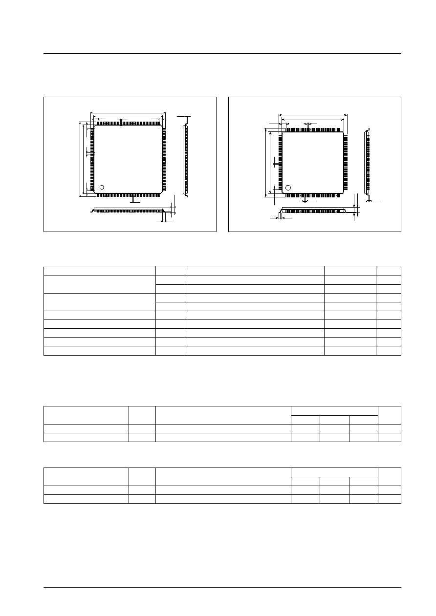
Package Dimensions
unit: mm
3230-SQFP176
3244-LQFP176
176
133
1
44
132
89
45
88
0.4
20.0
(1.4)
(0.5)
22.0
0.5
0.15
1.6max
0.4
20.0
(1.4)
22.0
0.1
(1.4)
0.125
SANYO: LQFP176
[LC895299L]
26.0
24.0
0.5
1.25
26.0
0.1
0.5
24.0
1.25
1
44
45
88
89
132
133
176
1.25
1.25
0.5
1.6max
1.4
0.2
0.5
0.125
SANYO: SQFP176
[LC895299W]
Parameter
Symbol
Conditions
Ratings
Unit
Maximum supply voltage
V
DD5
max
Ta = 25∞C
≠0.3 to +6.0
V
V
DD3
max
Ta = 25∞C
≠0.3 to +4.6
V
Input and output voltages
V
I5
, V
O5
Ta = 25∞C
≠0.3 to V
DD5
+ 0.3
V
V
I3
, V
O3
Ta = 25∞C
≠0.3 to V
DD3
+ 0.3
V
Allowable power dissipation
Pd max
Ta
70∞C
550
mW
Operating temperature
Topr
≠30 to +70
∞C
Storage temperature
Tstg
≠55 to +125
∞C
Soldering conditions (pins only)
10 seconds
235
∞C
Input and output power
I
I
, I
O
±20
*
mA
Specifications
Absolute Maximum Ratings
at V
SS
= 0 V
Note:
*
Per single input or output basic cell.
Parameter
Symbol
Conditions
Ratings
Unit
min
typ
max
Supply voltage
V
DD
4.5
5.0
5.5
V
Input voltage range
V
IN
0
V
DD
V
Allowable Operating Ranges
at Ta = 0 to +70∞C, V
SS
= 0 V
I/O Cell 5.0-V Power Supply
Parameter
Symbol
Conditions
Ratings
Unit
min
typ
max
Supply voltage
V
DD
3.0
3.3
3.8
V
Input voltage range
V
IN
0
V
DD
V
Internal Cell 3.3-V Power Supply
Note: The input voltage range for speeds of 45
◊
or over is 4.5 to 5.25 V.
Note: The input voltage range differs depending on the drive speed used. Contact your Sanyo representative for details.

No. 6249-3/12
LC895299W, 895299L
Parameter
Symbol
Conditions
Applicable pins
*
Ratings
Unit
min
typ
max
Input high-level voltage
V
IH
TTL level inputs
1
2.2
V
Input low-level voltage
V
IL
0.8
V
Input high-level voltage
V
IH
TTL level inputs with pull-up resistors
7
2.2
V
Input low-level voltage
V
IL
0.8
V
Input high-level voltage
V
IH
TTL level inputs with pull-down resistors
2
2.2
V
Input low-level voltage
V
IL
0.8
V
Input high-level voltage
V
IH
TTL level inputs
3, 9
2.4
V
Input low-level voltage
V
IL
Schmitt inputs
0.8
V
Input high-level voltage
V
IH
TTL level inputs
19, 20
2.4
V
Input low-level voltage
V
IL
Schmitt inputs with pull-up resistors
0.8
V
Input high-level voltage
V
IH
CMOS level inputs
4
0.8 V
DD
V
Input low-level voltage
V
IL
Schmitt inputs
0.2 V
DD
V
Input high-level voltage
V
IH
CMOS level inputs with pull-up resistors
5
0.7 V
DD
V
Input low-level voltage
V
IL
0.3 V
DD
V
Analog input voltage
V
ANI
18
1/4 V
DD
3/4 V
DD
V
Output high-level voltage
V
OH
I
OH
= ≠2 mA
6, 17
V
DD
≠ 2.1
V
Output low-level voltage
V
OL
I
OL
= 2 mA
0.4
V
Output high-level voltage
V
OH
I
OH
= ≠8 mA
7, 8, 14
V
DD
≠ 2.1
V
Output low-level voltage
V
OL
I
OL
= 8 mA
0.4
V
Output high-level voltage
V
OH
I
OH
= ≠4 mA
9, 12, 10, 20
V
DD
≠ 2.1
V
Output low-level voltage
V
OL
I
OL
= 24 mA
0.4
V
Output high-level voltage
V
OH
I
OH
= ≠4 mA
16
V
DD
≠ 2.1
V
Output low-level voltage
V
OL
I
OL
= 4 mA
0.4
V
Output low-level voltage
V
OL
I
OL
= 24 mA
11, 21
0.4
V
Output low-level voltage
V
OL
I
OL
= 1 mA
13
0.4
V
Output low-level voltage
V
OL
I
OL
= 8 mA
15
0.4
V
Analog output voltage
V
ANO
22
1/4 V
DD
3/4 V
DD
V
Input leakage current
I
IL
V
I
= V
SS
, V
DD
1, 3, 4, 9
≠10
+10
µA
Output leakage current
I
OZ
During high-impedance output
9, 11, 13,
≠10
+10
µA
14, 16, 17
Pull-up resistance
R
UP
5
50
100
200
k
Pull-up resistance
R
UP
7, 15
20
40
80
k
Pull-up resistance
R
UP
19, 20, 21
7
10
13
k
Pull-down resistance
R
DN
2
50
100
200
k
Pull-down resistance
R
DN
10
7
10
13
k
DC Characteristics
at Ta = 0 to +70∞C, V
SS
= 0 V, V
DD
= 4.5 to 5.5 V
Note:
*
The applicable pin column entries refer to the following sets.
INPUT
1 :
ATPINSEL, SUA0 to SUA7
2 :
TEST0 to TEST2
3 :
DA0 to DA2, ZCS1FX, ZCS3FX, ZDIOR, ZDIOW, ZHRST, ZCS, ZRD, ZWR
4 :
ZRESET, ZDSPRST
5 :
FG
18 : AD0, AD1, PH, BH, RREC, FE, TE, VREF, CSS, AD2
19 : ZDMACK, CSEL
OUTPUT
6 :
FSEQ
8 :
HFLO, FSX, EFLG, C2F, WRQ, DIR, PCK, EFMOUT
13 : HINTRQ
11 : ZIOCS16
10 : DMARQ
13 : PDS1 to PDS3
14 : DOUT
15 : ZSWAIT, ZINT0, ZINT1
21 : IORDY
16 : DSLB, EQS, OUTPORT0 to OUTPORT2, MCK
17 : RHLD, TSH, BHH, GHS, LDON
22 : PHC, BHC, FBAL, TBAL, SGC, TOFST, TDO, FDO, SLDO, SPDO
INOUT
7 :
D0 to D7, TRV, TRV2
9 :
DD0 to DD15
20 : ZDASP, ZPDIAG
Note: XTAL, XTALCK
The above pins are not included in the DC Characteristics.
No. 6249-4/12
LC895299W, 895299L
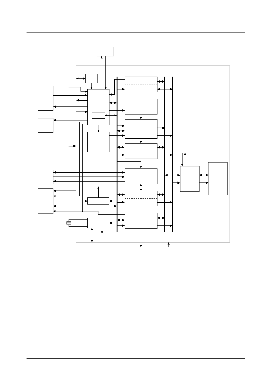
Block Diagram
Sub-code
SYNC
Detector
De-scramble
&
Buffering
Address generator
Micro controller
RAM access
Address generator
Address generator
ECC & EDC
I/F
ATAPI
Address generator
Data output input I/F
Address generator
CAV-AUDIO
Bus Arbiter
&
DRAM
controller
Buffer
DRAM
Each Block
Bus control
signal
Each Block
Register
CD-DSP I/F
&
SYNC
Detector
SRAM
CD-DSP
LA9238
HOST
Audio
Circuit
VCEC
PLL
Driver
FG
TDO, FDO
SLDO, SPDO
Micro
controller
decoder
PLL Clock
generator
*11
*1
*12
*2
*14
*3
*4
*5
*6
*7
*8
WRQ
ZSWAIT
ZINT 1
ZINT 0
ZRESET
ZDSPRST
*13
*9
*10
XTALCK
XTAL
Each Block
Data bus[0:7]
Address bus[0:18]
DRAM
Data bus[0:15]
A12530
*
1
EFMIN, EFMIN2, PH, BH, FE, TE, TES, RREC
*
2
RHLD, TSH, EQS, BHH, GHS, LDON, FBAL, TBAL, TOFST, SGC
*
3
LOUT, ROUT, DOUT
*
4
DD0 to DD15, ZDASP, ZPDIAG
*
5
ZCS1FX, ZCS3FX, DA0 to DA2, ZDIOR, ZDIOW, ZDMACK, ZHRST, CSEL
*
6
DMARQ, HINTRQ, ZIOCS16, IORDY
*
7
ZRD, ZWR, ZCS, CSCTRL, SUA0 to SUA7
*
8
D0 to D7
*
9
DIR/FLOCK, HFLO/TLOCK, FSEQ, FSX/LRCK, EFLG/CK2, C2F, EFMOUT, PCK, TRV2/DATA, TRV, PORT OUT0 to OUT2
*
10 ATPINSEL, TEST0 to TEST2
*
11 RPO, OPP, PCKISTF, PCKISTP, PDO, POS1 to POS3, FR
*
12 SLCO0 to SLCO3, JITC, DSLB, PHC, BHC
*
13 PLL1 to PLL3
*
14 SLCIT1 to SLCIT2, JITIN, AD0 to AD2, VREF, CSS
No. 6249-5/12
LC895299W, 895299L
Pin Functions
LC895299 Pin Functions 1
(When pin 95, ATPINSEL, is low)
Type
I
INPUT
B
BIDIRECTION
NC
NOT CONNECT
O
OUTPUT
P
POWER
Pin No.
Pin
Type
Function
1
V
SS
P
Logic system ground
2
FLOCK/CRCERR
O
Monitor outputs
3
DIR/TLOCK
O
4
ZSWAIT
O
Wait signal output to the microcontroller
5
WRQ/HFLO
O
Monitor output
6
ZINT0
O
Microcontroller interrupt
7
ZINT1
O
8
TEST0
I
Test pin (Must be tied to ground during normal operation.)
9
D0
B
10
D1
B
11
D2
B
12
D3
B
13
D4
B
Microcontroller data bus
14
D5
B
15
D6
B
16
D7
B
17
MCK
O
Clock output to the microcontroller
18
ZCS
I
Microcontroller ZCS signal
19
NC
20
NC
21
V
DDD
P
DRAM V
DD
: 5 V
22
V
DD1
P
3.3 V
23
V
SS
P
Logic system ground
24
V
SSD
P
DRAM ground
25
NC
26
NC
27
SUA0
I
28
SUA1
I
29
SUA2
I
30
SUA3
I
Microcontroller address bus
31
SUA4
I
32
SUA5
I
33
SUA6
I
34
SUA7
I
35
ZWR
I
Microcontroller write signal
36
ZRD
I
Microcontroller read signal
37
FSEQ
O
Frame synchronization detection
38
DOUT/TESO
O
Digital output/tes output
39
V
DD0
P
I/O system power supply: 5 V
40
V
SS
P
Logic system ground
41
PLL1
I
42
PLL2
I
System Clock PLL
43
PLL3
O
44
PLL1 V
DD
P
Logic PLL V
DD
: 3.3 V
45
PLL1 V
SS
P
Logic PLL system ground
46
CSEL
I
47
ZHRST
I
48
ZDASP
B
ATAPI I/F
49
ZCS3FX
I
50
ZCS1FX
I
51
V
SS1
I
I/F ground
52
V
DD0
I
I/O system power supply: 5 V
Continued on next page.