
Overview
Now, thick-film audio power amplifier ICs are available
with pin-compatibility to permit a single PCB to be
designed and amplifier output capacity changed simply by
installing a hybrid IC. This new series was developed
with this kind of pin-compatibility to ensure integration
between systems everywhere. With this new series of IC,
even changes from 3-channel amplifier to 2-channel
amplifiers are possible using the same PCB. In addition,
this new series of ICs has a 6/3
drive in order to support
the low impedance of modern speakers.
Features
∑ Pin-compatible
STK400-000 series (3-channel, single package)
STK401-000 series (2-channel, single package)
∑ Output load impedance RL=6
/3
supported
∑ New pin assignment
To simplify input/output pattern layout and minimize
the effects of pattern layout on operational
characteristics, pin assignments are grouped into blocks
consisting of input, output and power systems.
∑ Few external circuits
Compared to those series used until now, capacitors and
bootstrap resistors for external circuits can be greatly
reduced.
Package Dimensions
unit : mm
4086A
Thick Film Hybrid IC
N3096 HA (OT)/D2894 TH(OT) No. 4830-1/10
[STK400-020]
SANYO Electric Co.,Ltd. Semiconductor Bussiness Headquarters
TOKYO OFFICE Tokyo Bldg., 1-10, 1 Chome, Ueno, Taito-ku, TOKYO, 110 JAPAN
3-Channel AF Power Amplifier (Split Power Supply)
(15 W + 15 W +15 W min, THD = 0.4 %)
STK400-020
Ordering number : EN4830A
•
Parameter
Symbol
Conditions
Ratings
Unit
Maximum supply voltage
V
CC
max
±29
V
Thermal resistance
j-c
Per power transistor
2.1
∞C/W
Junction temperature
Tj
150
∞C
Operating substrate temperature
Tc
125
∞C
Storage temperature range
Tstg
≠30 to +125
∞C
Permissible load short time
t
s
V
CC
= ±20 V, R
L
= 6
, f = 50 Hz, P
O
= 15 W
1
s
Specifications
Maximum Ratings
at Ta = 25∞C
Operating Characteristics
at Ta = 25∞C, R
L
= 6
, Rg = 600
, VG = 40 dB, R
L
(noninductive)
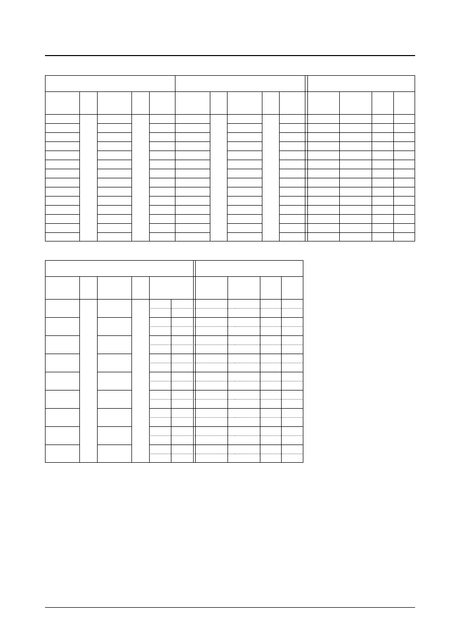
Internal Equivalent Circuit
Notes
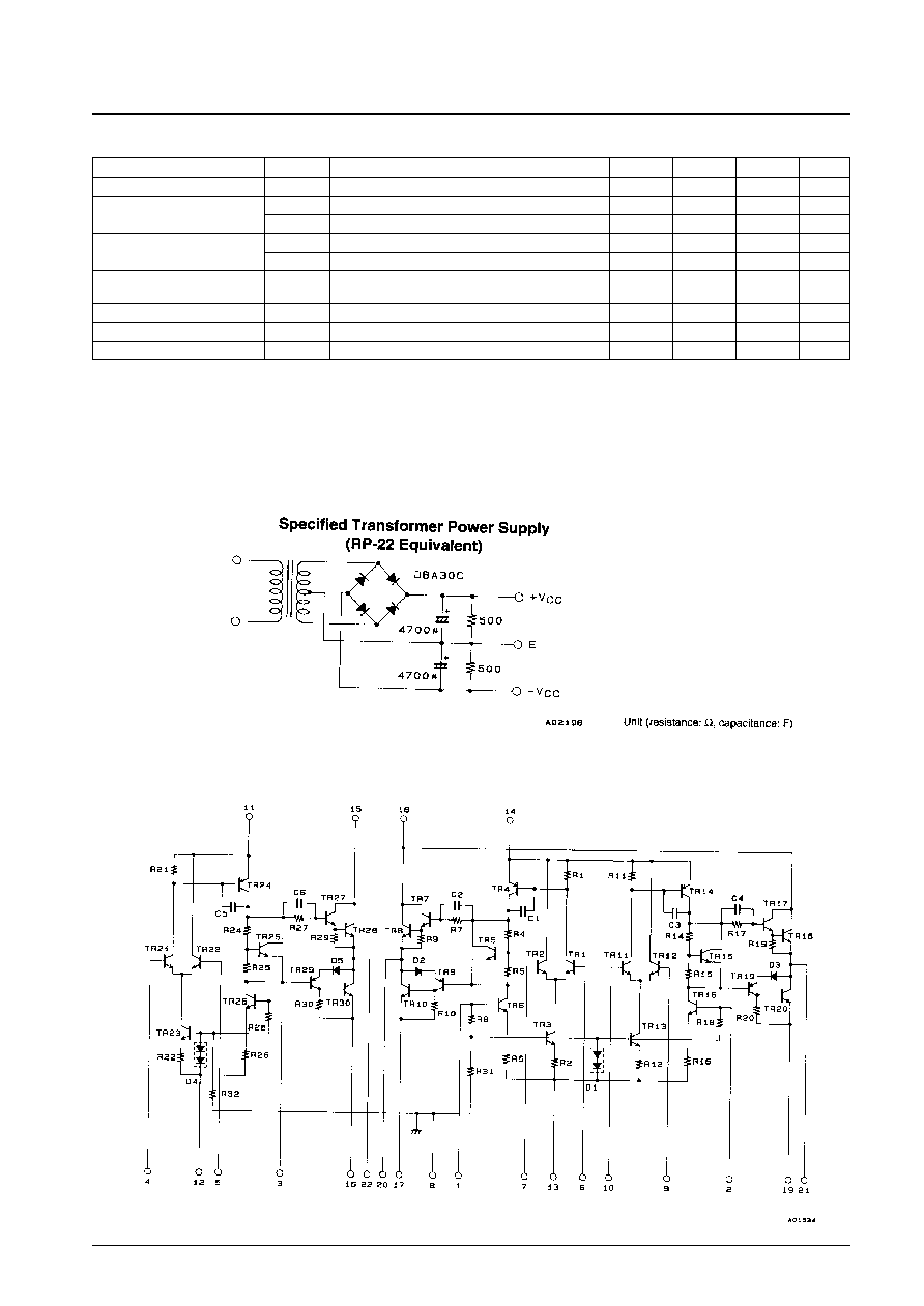
∑ Use rated power supply for testing unless otherwise specified.
∑ When measuring permissible load short time and output noise voltage, use transformer power supply indicated below.
∑ Output noise voltage is represented by the peak value rms (VTVM) for mean reading. Use an AC stabilized power
supply (50 Hz) on the primary side to eliminate the effect of AC flicker noise.
No. 4830-2/10
STK400-020
Parameter
Symbol
Conditions
min
typ
max
Unit
Quiescent current
I
CCO
V
CC
=± 24 V
30
90
150
mA
Output power
P
O
(1)
V
CC
= ±20 V, f = 20 Hz to 20 kHz, THD = 0.4%
15
20
W
P
O
(2)
V
CC
= ±16 V, f = 1 kHz, THD = 1.0%, R
L
= 3
15
20
W
Total harmonic distortion
THD (1)
V
CC
= ±20 V, f = 20 Hz to 20 kHz, P
O
= 1.0 W
0.4
%
THD (2)
V
CC
= ±20 V, f = 1 kHz, P
O
= 5.0 W
0.02
%
Frequency response
f
L
, f
H
V
CC
= ±20 V, P
O
= 1.0 W,
dB
20 to 50 k
Hz
Input impedance
r
i
V
CC
= ±20 V, f = 1 kHz, P
O
= 1.0 W
55
k
Output noise voltage
V
NO
V
CC
= ±24 V, Rg = 10 k
1.2
mVrms
Neutral voltage
V
N
V
CC
= ±24 V
≠70
0
+70
mV
+0
≠3

Pattern Example for PCB Used with Either 2- or 3-Channel Amplifiers
Sample Application Circuit
No. 4830-3/10
STK400-020

No. 4830-4/10
STK400-020
Description of External Circuits
C1, 11, 21
For input coupling capacitor. Used for current blocking. When capacitor reactance with low frequency is increased, the reactance value
should be reduced in order to reduce the output noise from the signal resistance dependent 1/f noise. In response to the popping noise
which occurs when the system power is turned on, C1 and C11 which determine the decay time constant on the input side are
increased while C3, C13 and C23 on the NF side are decreased.
C2, 12, 22
For input filter capacitor. Permits high-region noise reduction by utilizing filter constructed with R1, R11 and R21.
C3, 13, 23
For NF capacitor. This capacitor determines the decline of the cutoff frequency and is calculated according to the following equation.
f
L
=
1
2
X C3 (13, 23,) X R3 (13, 23)
For the purpose of achieving voltage gains prior to reduction, it is best that C3, C13 and C23 are large. However, because the shock
noise which occurs when the system power is turned on tends to increase, values larger than those absolutely necessary should be
avoided.
C5, 15, 25
For oscillation prevention capacitor. A Mylar capacitor with temperature and frequency features is recommended.
C6, 7
For oscillation prevention capacitor. To ensure safe IC functioning, the capacitor should be installed as close as possible to the IC
power pin to reduce power impedance. An electrolytic capacitor is good.
C8, 9, 28, 29
For decoupling capacitor. Reduces shock noise during power-up using decay time constant circuits with R8, R9, R28 and R29 and
eliminates components such as ripples crossing over into the input side from the power line.
R1, 11, 21
For input filter applied resistor.
R2, 12, 22
For input bias resistor. The input pin is biased to zero potential. Input impedance is mostly decided with this resistance value.
R3, 13, 23
For resistors to determine voltage gain (VG). We recommend a VG = 40 dB using R3, R13, R23 = 560
and R4, R14 and R24 = 56
.
VG adjustments are best performed using R3, R13 and R23. When using R4, R14 and R24 for such purposes, R4, R14 and R24
should be set to equal R2, R12 and R22 in order to establish a stable VN balance.
R5, 15, 25
For oscillation prevention resistor.
R6, 16, 26
For oscillation prevention resistor. This resistor's electrical output resides in the signal frequency and is calculated according to the
following formula.
P R6 (16, 26) =
(
V
CC
max/
2
)
2
◊
R6 (16, 26)
1/2
fC5 (15, 25) + R6 (16, 26)
f = output signal frequency upper limit
R8, 9, 28, 29
For ripple filter applied resistor. P
O
max, ripple rejection and power-up shock noise are modified according to this value. Set the
electrical output of these resistors while keeping in mind the flow of peak current during recharging to C8, C9, C28 and C29 which
function as pre-drive TR control resistors during load shorts.
L1, 2, 3
For oscillation prevention coil. Compensates phase dislocation caused by load capacitors and ensures stable oscillation.
R4, 14, 24
Series Configuration
No. 4830-5/10
STK400-020
STK400-000, STK400-200 series
STK401-000, STK401-200 series (2-channel)
Supply voltage (V)
(3-channel identical output)
THD
THD
Fixed
THD
THD
Fixed
IC name
(%)
IC name
(%)
standard
IC name
(%)
IC name
(%)
standard
V
CC
max1
V
CC
max2
V
CC
1
V
CC
2
output
output
STK400-010
STK400-210
10 W
◊
3
STK401-010
STK401-210
10 W
◊
2
--
±26.0
±17.5
±14.0
STK400-020
STK400-220
15 W
◊
3
STK401-020
STK401-220
15 W
◊
2
--
±29.0
±20.0
±16.0
STK400-030
STK400-230
20 W
◊
3
STK401-030
STK401-230
20 W
◊
2
--
±34.0
±23.0
±19.0
STK400-040
STK400-240
25 W
◊
3
STK401-040
STK401-240
25 W
◊
2
--
±36.0
±25.0
±21.0
STK400-050
STK400-250
30 W
◊
3
STK401-050
STK401-250
30 W
◊
2
--
±39.0
±26.0
±22.0
STK400-060
STK400-260
35 W
◊
3
STK401-060
STK401-260
35 W
◊
2
--
±41.0
±28.0
±23.0
STK400-070
0.4
STK400-270
0.08
40 W
◊
3
STK401-070
0.4
STK401-270
0.08
40 W
◊
2
--
±44.0
±30.0
±24.0
STK400-080
STK400-280
45 W
◊
3
STK401-080
STK401-280
45 W
◊
2
--
±45.0
±31.0
±25.0
STK400-090
STK400-290
50 W
◊
3
STK401-090
STK401-290
50 W
◊
2
--
±47.0
±32.0
±26.0
STK400-100
STK400-300
60 W
◊
3
STK401-100
STK401-300
60 W
◊
2
--
±51.0
±35.0
±27.0
STK400-110
STK400-310
70 W
◊
3
STK401-110
STK401-310
70 W
◊
2
±56.0
--
±38.0
--
STK401-120
STK401-320
80 W
◊
2
±61.0
--
±42.0
--
STK401-130
STK401-330
100 W
◊
2
±65.0
--
±45.0
--
STK401-140
STK401-340
120 W
◊
2
±74.0
--
±51.0
--
STK400-400, STK400-600 series
Supply voltage (V)
(3-channel differing output)
THD
THD
Fixed
IC name
(%)
IC name
(%)
standard
V
CC
max1
V
CC
max2
V
CC
1
V
CC
2
output
STK400-450
STK400-650
C ch
30 W
--
±39.0
±26.0
±22.0
L, R ch
15 W
--
±29.0
±20.0
±16.0
STK400-460
STK400-660
C ch
35 W
--
±41.0
±28.0
±23.0
L, R ch
15 W
--
±29.0
±20.0
±16.0
STK400-470
STK400-670
C ch
40 W
--
±44.0
±30.0
±24.0
L, R ch
20 W
--
±34.0
±23.0
±19.0
STK400-480
STK400-680
C ch
45 W
--
±45.0
±31.0
±25.0
L, R ch
20 W
--
±34.0
±23.0
±19.0
STK400-490
0.4
STK400-690
0.08
C ch
50 W
--
±47.0
±32.0
±26.0
L, R ch
25 W
--
±36.0
±25.0
±21.0
STK400-500
STK400-700
C ch
60 W
--
±51.0
±35.0
±27.0
L, R ch
30 W
--
±39.0
±26.0
±22.0
STK400-510
STK400-710
C ch
70 W
±56.0
--
±38.0
--
L, R ch
35 W
--
±41.0
±28.0
±23.0
STK400-520
STK400-720
C ch
80 W
±61.0
--
±42.0
--
L, R ch
40 W
--
±44.0
±30.0
±24.0
STK400-530
STK400-730
C ch
100 W
±65.0
--
±45.0
--
L, R ch
50 W
--
±47.0
±32.0
±26.0
V
CC
max1
R
L
= 6
V
CC
max2
R
L
= 6
to 3
operation
V
CC
1
R
L
= 6
operation
V
CC
2
R
L
= 3
operation