 | –≠–ª–µ–∫—Ç—Ä–æ–Ω–Ω—ã–π –∫–æ–º–ø–æ–Ω–µ–Ω—Ç: STK4172II | –°–∫–∞—á–∞—Ç—å:  PDF PDF  ZIP ZIP |
STK4172
II
SANYO Electric Co., Ltd. Semiconductor Business Headquarters
TOKYO OFFICE Tokyo Bldg., 1-10, 1 Chome, Ueno, Taito-ku, TOKYO, 110 JAPAN
70997HA (ID) / O138YT / 9068MO, TS No. 2323--1/8
Ordering number: EN2323A
Thick Film Hybrid IC
AF Power Amplifier (Split Power Supply)
(40W + 40W min, THD = 0.4%)
Features
∑ The STK4102II series (STK4172II) and STK4101V
series (high-grade type) are pin-compatible in the out-
put range of 6W to 50W and enable easy design.
∑ Small-sized package whose pin assignment is the same
as that of the STK4101II series
∑ Built-in muting circuit to cut off various kinds of pop
noise
∑ Greatly reduced heat sink due to substrate temperature
125
∞
C guaranteed
∑ Excellent cost performance
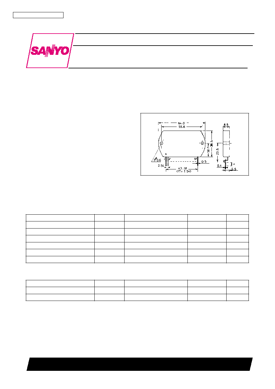
Package Dimensions
unit: mm
4040
[STK4172
II
]
Specifications
Maximum Ratings
at Ta = 25
∞
C
Recommended Operating Conditions
at Ta = 25
∞
C
Parameter
Symbol
Conditions
Ratings
Unit
Maximum supply voltage
V
CC
max
±
48
V
Thermal resistance
j-c
1.8
∞
C/W
Junction Temperature
Tj
150
∞
C
Operating substrate temperature
Tc
125
∞
C
Storage temperature
Tstg
-
30 to +125
∞
C
Available time for load short-circuit
ts
V
CC
=
±
32V, R
L
= 8
, f = 50Hz, Po = 40W
2
s
Parameter
Symbol
Conditions
Ratings
Unit
Recommended supply voltage
V
CC
±
32
V
Load resistance
R
L
8
STK4172
II
No. 2323--2/8
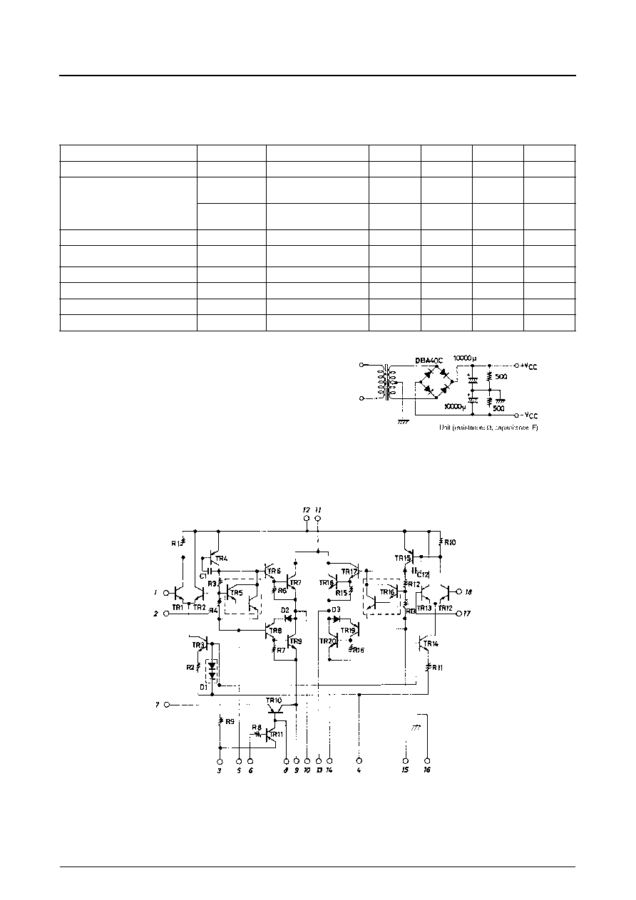
Notes.
For power supply at the time of test, use a constant-voltage power supply
unless otherwise specified.
For measurement of the available time for load short-circuit and output
noise voltage, use the specified transformer power supply shown right.
The output noise voltage is represented by the peak value on rms scale
(VTVM) of average value indicating type. For AC power supply, use an
AC stabilized power supply (50Hz) to eliminate the effect of flicker noise
in AC primary line.
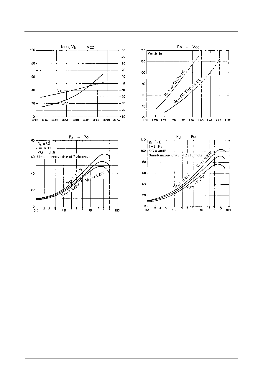
Operating Characteristics
at Ta = 25
∞
C, V
CC
=
±
32V, R
L
= 8
, Rg = 600
, VG = 40dB,
R
L
: non-inductive load
Parameter
Symbol
Conditions
min
typ
max
Unit
Quiescent current
I
CCO
V
CC
=
±
38.5V
20
40
100
mA
Output power
P
O
(1)
THD = 0.4%,
f = 20Hz to 20kHz
40
W
P
O
(2)
V
CC
=
±
29V, THD = 1.0%,
R
L
= 4
, f = 1kHz
45
W
Total harmonic distortion
THD
P
O
= 1.0W, f = 1kHz
0.3
%
Frequency response
f
L
, f
H
P
O
= 1.0W,
dB
20 to 50k
Hz
Input impedance
r
i
P
O
= 1.0W, f = 1kHz
55
k
Output noise voltage
V
NO
V
CC
=
±
38.5V, Rg = 10k
1.2
mVrms
Neutral voltage
V
N
V
CC
=
±
38.5V
≠70
0
+70
mV
Muting voltage
V
M
≠2
≠5
≠10
V
+0
≠3
Specified Transformer Power Supply
(Equivalent to MG-200)
Equivalent Circuit
STK4172
II
No. 2323--3/8
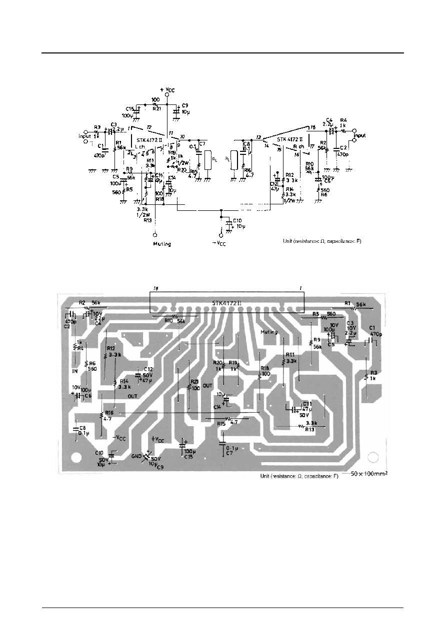
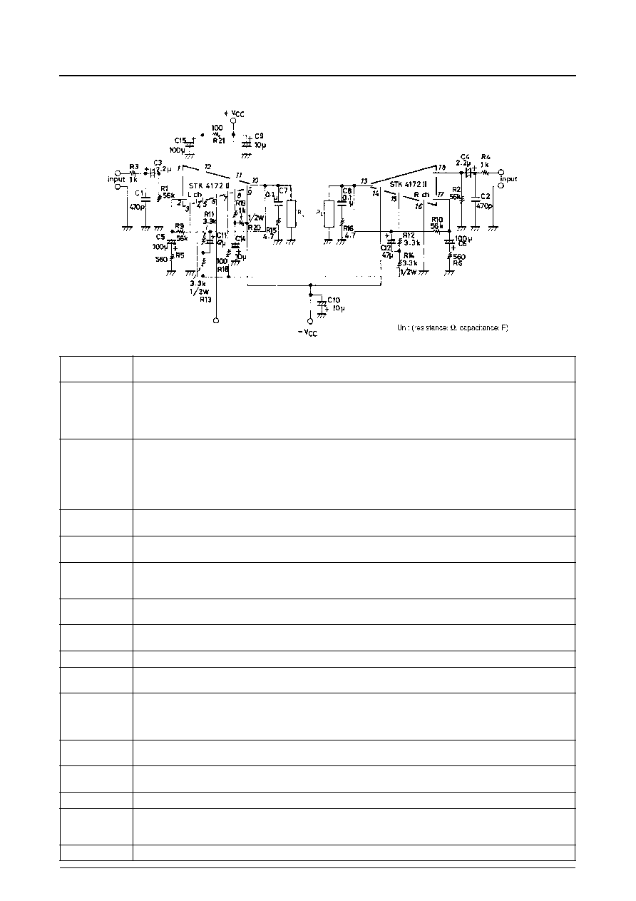
Sample Application Circuit (I)
40W min 2-channel AF power amplifier
Sample Printed Circuit Pattern for Application Circuit
(Cu-foiled side)
STK4172
II
No. 2323--4/8
Input voltage, Vi - mV
Output power, Po - W
Frequency, f - Hz
Output po
wer
, Po -
W
T
otal harmonic distortion,
THD - %
V
oltage g
ain,
V
G
- dB
Output power, Po - W
Frequency, f - Hz
Operating substrate temperature, Tc -
∞
C
T
otal harmonic distortion,
THD - %
Output po
wer
, Po -
W
Quiescent current, Icco - mA
Neutral v
oltage,
V
N
- mV
STK4172
II
No. 2323--5/8
Supply voltage, V
CC
- V
Output power, Po - W
Quiescent current, Icco - mA
Neutral v
oltage,
V
N
- mV
IC po
wer dissipation, Pd -
W
Supply voltage, V
CC
- V
Output power, Po - W
Output po
wer
, Po -
W
IC po
wer dissipation, Pd -
W
STK4172
II
No. 2323--6/8
Description of External Parts
C1, C2
Input filter capacitors
∑ A filter formed with R3 or R4 can be used to reduce noise at high frequencies.
C3, C4
Input coupling capacitors
∑ Used to block DC current. When the reactance of the capacitor increases at low frequencies, the dependence of 1/f noise on signal source
resistance causes the output noise to worsen. It is better to decrease the reactance.
∑ To reduce the pop noise at the time of application of power, it is effective to increase C3, C4 that fix the time constant on the input side and
to decrease C5, C6 on the NF side.
C5, C6
NF capacitors
∑ These capacitors fix the low cutoff frequency as shown below.
To provide the desired voltage gain at low frequencies, it is better to increase C5. However, do not increase C5 more than needed because
the pop noise level becomes higher at the time of application of power.
C15
Decoupling capacitor
∑ Used to eliminate the ripple components that mix into the input side from the power line (+V
CC
).
C11, C12
Bootstrap capacitors
∑ When the capacitor value is decreased, the distortion is liable to be higher at low frequencies.
C9, C10
Oscillation blocking capacitors
∑ Must be inserted as close to the IC power supply pins as possible so that the power supply impedance is decreased to operate the IC stably.
∑ Electrolytic capacitors are recommended for C9, C10.
C14
Capacitor for ripple filter
∑ Capacitor for the TR10-used ripple filter in the IC system
C7
Oscillation blocking capacitor
∑ A polyester film capacitor, being excellent in temperature characteristic, frequency characteristic, is recommended for C7.
R3, R4
Resistors for input filter
R1, R2
Input bias resistors
∑ Used to bias the input pin potential to zero. These resistors fix the input impedance practically.
R5, R9
(R6, R10)
These resistors fix voltage gain VG.
It is recommended to use R5 (R6) = 560
, R9 (R10) = 56k
for VG = 40dB.
∑ To adjust VG, it is desirable to change R5 (or R6).
∑ When R5 (or R6) is changed to adjust VG, R1 (=R2) =R9 (=R10) must be set to ensure V
N
balance.
R11, R13
(R12, R14)
Bootstrap resistors
∑ The quiescent current is set by these resistors 3.3k
+ 3.3k
. It is recommended to use this resistor value.
R21
Resistor for ripple filter
∑ (Limiting resistor for predriver transistor at the time of load short)
R18
Used to ensure plus/minus balance at the time of clip.
R19, R20
Resistor for ripple filter
∑ When muting TR11 is turned ON, current flows from ground to -V
CC
through TR 11. It is recommended to use 1k
(1W) + 1k
(1W)
allowing for the power that may be dissipated on that occasion.
R15, R16
Oscillation blocking resistors
f
L
1
2
C5 R5
--------------------------
=
[Hz]
STK4172
II
No. 2323--7/8
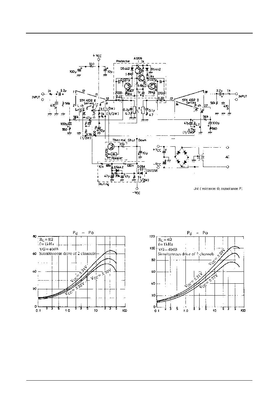
Sample Application Circuit (II)
(protection circuit and muting circuit)
Thermal Design
The IC power dissipation of the STK4172II at the IC-operated mode is 55W max. at load resistance 8
and 91W max. at
load resistance 4
(simultaneous drive of 2 channels) for continuous sine wave as shown in Figure 1 and 2.
Figure 1. STK4172II Pd ≠ Po (R
L
= 8
)
Figure 2. STK4172II Pd ≠ Po (R
L
= 4
)
Output power, Po - W
IC Po
wer dissipation, Pd -
W
Output power, Po - W
IC Po
wer dissipation, Pd -
W
STK4172
II
No. 2323--8/8
s
No products described or contained herein are intended for use in surgical implants, life-support systems, aerospace equipment, nuclear
power control systems, vehicles, disaster/crime-prevention equipment and the like, the failure of which may directly or indirectly cause injury,
death or property loss.
s
Anyone purchasing any products described or contained herein for an above-mentioned use shall:
Accept full responsibility and indemnify and defend SANYO ELECTRIC CO., LTD., its affiliates, subsidiaries and distributors and all their
officers and employees, jointly and severally, against any and all claims and litigation and all damages, cost and expenses associated
with such use:
Not impose any responsibility for any fault or negligence which may be cited in any such claim or litigation on SANYO ELECTRIC CO.,
LTD., its affiliates, subsidiaries and distributors or any of their officers and employees, jointly or severally.
s
Information (including circuit diagrams and circuit parameters) herein is for example only; it is not guaranteed for volume production. SANYO
believes information herein is accurate and reliable, but no guarantees are made or implied regarding its use or any infringements of
intellectual property rights or other rights of third parties.
This catalog provides information as of July, 1997. Specifications and information herein are subject to change without notice.
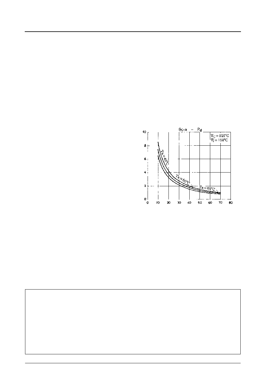
In an actual application where a music signal is used, it is impractical to estimate the power dissipation based on the con-
tinuous signal as shown above, because too large a heat sink must be used. It is reasonable to estimate the power dissipa-
tion as 1/10 Po max. (EIAJ).
That is, Pd = 35W at 8
, Pd = 49W at 4
Thermal resistance
c-a of a heat sink for this IC power dissipation (Pd) is fixed under conditions 1 and 2 shown below.
Condition 1: Tc
= Pd
◊
c-a + Ta
125
∞
C............................................... (1)
where
Ta : Specified ambient temperature
Tc : Operating substrate temperature
Condition 2: Tj= Pd
◊ (
c-a) + Pd/4
◊ (
j-c) + Ta
150
∞
C..................... (2)
where
Tj : Junction temperature of power transistor
Assuming that the power dissipation is shared equally among the four power transistors (2 channels
◊
2), thermal resis-
tance
j-c is 1.8
∞
C/W and
Pd
◊ (
c-a + 1.8/4) + Ta
150
∞
C ........................................ (3)
Thermal resistance
c-a of a heat sink must satisfy ine-
qualities (1) and (3).
Figure 3 shows the relation between Pd and
c-a given
from (1) and (3) with Ta as a parameter.
[Example] The thermal resistance of a heat sink is
obtained when the ambient temperature speci-
fied for a stereo amplifier is 50
∞
C.
Assuming V
CC
=
±
32V, R
L
= 8
,
V
CC
=
±
29V, R
L
= 4
,
R
L
= 8
: Pd1 = 35W at 1/10 Po max.
R
L
= 4
: Pd2 = 49W at 1/10 Po max.
The thermal resistance of a heat sink is
obtained from Figure 3.
R
L
= 8
:
c-a1 = 2.15
∞
C/W
R
L
= 4
:
c-a2 = 1.53
∞
C/W
Tj when a heat sink is used is obtained from
(3).
R
L
= 8
: Tj = 141
∞
C
R
L
= 4
: Tj = 147
∞
C
Figure 3. STK4172II
c-a ≠ Pd
IC Power dissipation, Pd - W
Thermal resistance of heat sink,
c-a -
∞
C/W