 | –≠–ª–µ–∫—Ç—Ä–æ–Ω–Ω—ã–π –∫–æ–º–ø–æ–Ω–µ–Ω—Ç: TND017SW | –°–∫–∞—á–∞—Ç—å:  PDF PDF  ZIP ZIP |
Any and all SANYO products described or contained herein do not have specifications that can handle
applications that require extremely high levels of reliability, such as life-support systems, aircraft's
control systems, or other applications whose failure can be reasonably expected to result in serious
physical and/or material damage. Consult with your SANYO representative nearest you before using
any SANYO products described or contained herein in such applications.
SANYO assumes no responsibility for equipment failures that result from using products at values that
exceed, even momentarily, rated values (such as maximum ratings, operating condition ranges,or other
parameters) listed in products specifications of any and all SANYO products described or contained
herein.
ExPD (Excellent Power Device)
Lowside Power Switch
Lamp, Solenoid, and Motor-Driving Applications
Ordering number:ENN6481A
TND017MP, TND017SW
SANYO Electric Co.,Ltd. Semiconductor Company
TOKYO OFFICE Tokyo Bldg., 1-10, 1 Chome, Ueno, Taito-ku, TOKYO, 110-8534 JAPAN
12501TS TA-3183/42000TS (KOTO) TA-2832 No.6481≠1/5
Absolute Maximum Ratings
at Ta = 25∞C
Features
∑ N-channel MOSFET built in.
∑ Overheat protection.
∑ Overcurrent protection.
(Self recovery type current
limiting function)
∑ Overvoltage protection.
∑ TND017SW incorporates two
sets of circuit.
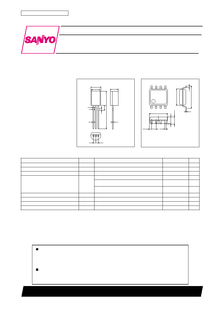
Package Dimensions
Unit:mm
2145
[TND017MP]
Package Dimensions
Unit:mm
2181
[TND017SW]
1 : GND1
2 : IN1
3 : GND2
4 : IN2
5 : OUT2
6 : OUT2
7 : OUT1
8 : OUT1
SANYO : SOP8
1 : GND
2 : OUT
3 : IN
SANYO : MP
∞C
∞C
∞C
0.5
0.6
0.5
5.0
6.0
6.0
3.0
8.5
14.0
4.7
1.45
1.45
1 2 3
0.5
1
4
5
8
4.4
0.3
6.0
0.2
5.0
0.595
1.27
1.5
0.1
1.8max
0.43
r
e
t
e
m
a
r
a
P
l
o
b
m
y
S
s
n
o
i
t
i
d
n
o
C
s
g
n
i
t
a
R
t
i
n
U
e
g
a
t
l
o
V
e
c
r
u
o
S
-
o
t
-
n
i
a
r
D
V S
D
0
6
V
t
n
e
r
r
u
C
t
u
p
t
u
O
IO
)
C
D
(
5
.
1
A
e
g
a
t
l
o
V
t
u
p
n
I
V N
I
0
1
+
o
t
3
.
0
≠
V
n
o
i
t
a
p
i
s
s
i
D
r
e
w
o
P
e
l
b
a
w
o
ll
A
PD
P
M
7
1
0
D
N
T
0
.
1
W
W
S
7
1
0
D
N
T
7
.
1
W
W
S
7
1
0
D
N
T
0
.
2
W
e
g
a
t
l
o
V
y
l
p
p
u
S
g
n
i
t
a
r
e
p
O
V S
D
)
r
p
o
(
0
4
V
e
r
u
t
a
r
e
p
m
e
T
g
n
i
t
a
r
e
p
O
r
p
o
T
5
8
+
o
t
0
4
≠
e
r
u
t
a
r
e
p
m
e
T
n
o
i
t
c
n
u
J
j
T
d
e
t
i
m
i
L
y
ll
a
n
r
e
t
n
I
e
r
u
t
a
r
e
p
m
e
T
e
g
a
r
o
t
S
g
t
s
T
0
5
1
+
o
t
5
5
≠
Mounted on a ceramic board (1200mm
2
◊
0.8mm) 1unit
Mounted on a ceramic board (1200mm
2
◊
0.8mm)
TND017MP, 017SW
No.6481≠2/5
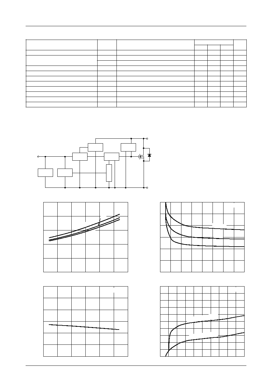
Block Diagram
∞C
Electrical Characteristics
at Ta = 25∞C
r
e
t
e
m
a
r
a
P
l
o
b
m
y
S
s
n
o
i
t
i
d
n
o
C
s
g
n
i
t
a
R
t
i
n
U
n
i
m
p
y
t
x
a
m
e
g
a
t
l
o
V
p
m
a
l
C
e
c
r
u
o
S
-
o
t
-
n
i
a
r
D
V S
D
p
m
a
l
c
V N
I
I
,
0
=
O
A
m
1
=
0
6
V
t
n
e
r
r
u
C
F
F
O
-
t
u
p
t
u
O
I
S
S
D
)
1
(
V N
I
V
,
0
=
S
D
V
0
5
=
0
1
A
µ
I
S
S
D
)
2
(
V N
I
V
,
0
=
S
D
V
2
1
=
5
A
µ
e
g
a
t
l
o
V
d
l
o
h
s
e
r
h
T
t
u
p
n
I
V N
I
)
h
t
(
V S
D
I
,
V
5
=
O
A
m
1
=
0
.
1
5
.
1
0
.
2
V
e
g
a
t
l
o
V
t
u
p
n
I
g
n
i
t
a
r
e
p
O
t
i
u
c
r
i
C
n
o
i
t
c
e
t
o
r
P
V N
I
)
r
p
o
(
4
0
1
V
e
c
n
a
t
s
i
s
e
R
N
O
e
c
r
u
o
S
-
o
t
-
n
i
a
r
D
R S
D
)
n
o
(
V N
I
I
,
V
5
=
O
A
1
=
3
.
0
4
.
0
)
N
O
t
u
p
t
u
O
(
t
n
e
r
r
u
C
t
u
p
n
I
I N
I
V N
I
V
5
=
5
2
.
0
6
.
0
A
m
e
r
u
t
a
r
e
p
m
e
T
g
n
i
t
c
e
t
e
D
t
a
e
h
r
e
v
O
)
d
s
(
j
T
V N
I
I
,
V
5
=
O
A
1
=
0
2
1
0
5
1
0
9
1
t
n
e
r
r
u
C
g
n
i
t
c
e
t
e
D
t
n
e
r
r
u
c
r
e
v
O
s
I
V N
I
V
5
=
0
.
3
0
.
4
0
.
5
A
)
k
a
e
P
(
t
i
m
i
L
t
n
e
r
r
u
c
r
e
v
O
I
T
M
L
V N
I
V
5
=
5
.
3
5
.
4
5
.
5
A
e
g
a
t
l
o
V
p
m
a
l
C
t
u
p
n
I
V N
I
p
m
a
l
c
,
I N
I
A
m
1
=
0
1
V
IN
GND(S)
OUT(D)
Gate
shutdown
Overcurrent
protection
Output current
control
Overvoltage
protection
Overheat
protection
ESD
protection
Latch
IIN -- Ta
IIN -- VIN
0
0.1
0.2
0.3
0.4
0.5
--50
--25
0
25
50
75
100
--50
--25
0
25
50
75
100
0
0.1
0.2
0.3
0.4
0.5
0.6
2
3
4
5
6
7
8
9
10
0
0.1
0.2
0.3
0.4
0.5
0.6
0.7
0.8
0.9
1.0
0
1
2
3
4
5
6
7
8
9
10
0
0.1
0.2
0.3
0.4
0.5
0.6
RDS(on) -- Ta
RDS(on) -- VIN
IT02013
IT02014
IT02011
IT02012
--40
∞
C
25
∞
C
Ta=85
∞
C
VIN
=4V
VIN=5V
6V
5V
IO=1A
IO=1A
Ta=25
∞
C
Input Current,
I IN
≠m
A
Input Current,
I IN
≠m
A
Protection operation
Normal operation
Input Voltage, VIN ≠ V
Input Voltage, VIN ≠ V
Ambient Temperature, Ta ≠ ∞C
Ambient Temperature, Ta ≠ ∞C
Drain-to-Source ON Resistance,
R
DS
(on)
≠
Drain-to-Source ON Resistance,
R
DS
(on)
≠
Notes : 1. Overcurrent protection circuit limits the output current to the range of overcurrent limit value.
2. During overheat protecting operation, output current is once turned off and then recovers after the input voltage falls to the reset voltage
(1.0V) or below.
TND017MP, 017SW
No.6481≠3/5
--50
--25
0
25
50
75
100
--50
--25
0
25
50
75
100
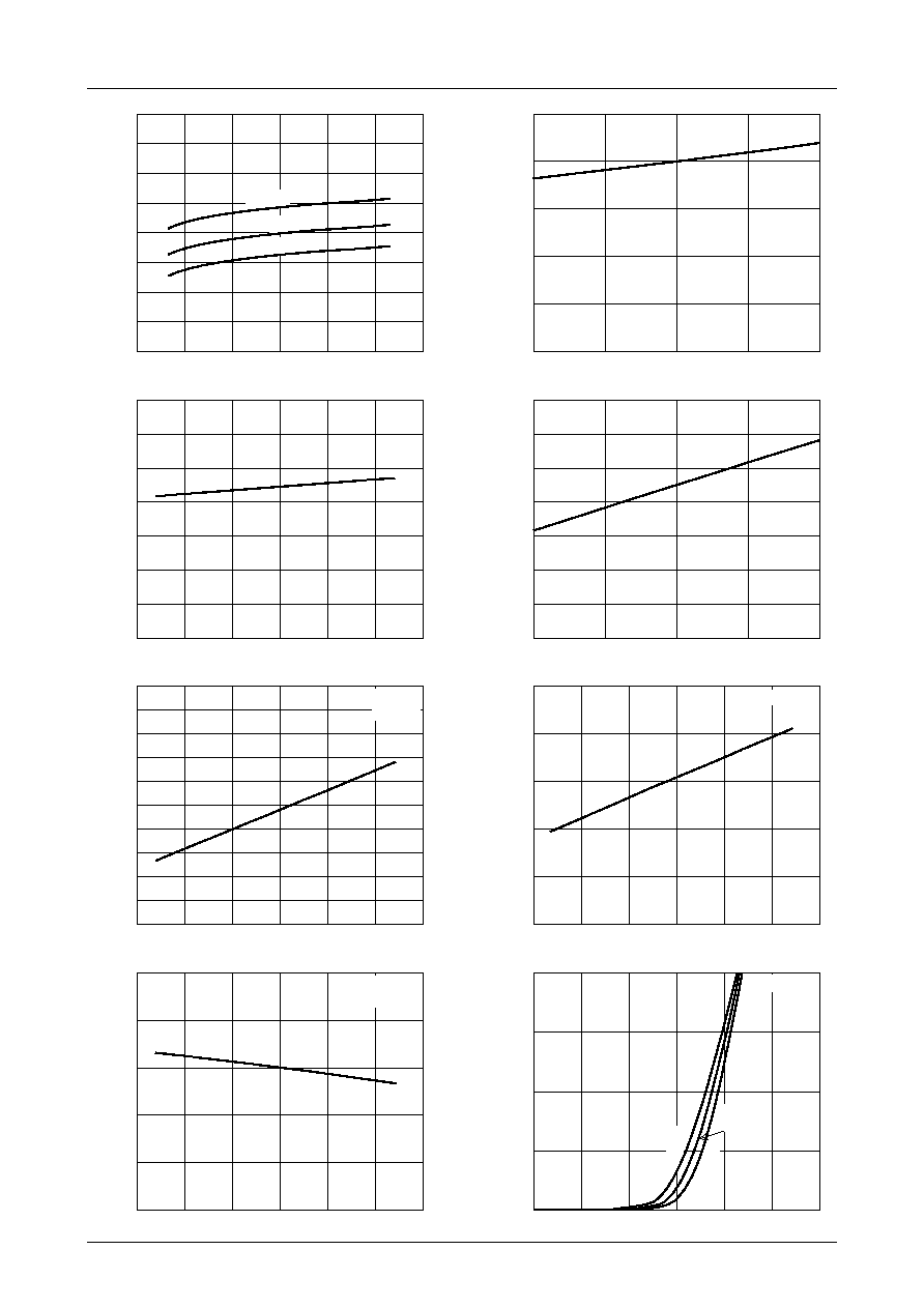
VDS=5V
IO=1mA
VIN(th) -- Ta
IT02021
VDS, clamp -- Ta
--50
--25
0
25
50
75
100
60
61
62
63
64
65
66
67
68
69
70
IT02019
IT02022
IT02020
10.0
10.5
11.0
11.5
12.0
12.5
VIN, clamp -- Ta
0.5
1.0
1.5
2.0
2.5
3.0
3.5
0
0.5
1.0
1.5
2.0
IO -- VIN
T
a=85
∞
C
IIN=1mA
VIN=0
IO=1mA
0
0.5
1.0
1.5
2.0
2.5
VDS=24V
--40
∞
C
25
∞
C
--50
--25
0
25
50
75
100
0
1
2
3
4
5
4.0
4.5
5.0
5.5
6.0
Is -- VIN
IT02016
Ta=25
∞
C
2.0
2.5
3.0
3.5
4.0
4.5
5.0
5.5
6.0
Is -- Ta
IT02015
--50
--25
0
25
50
75
100
0
1
2
3
4
5
6
7
0
1
2
3
4
5
6
7
ILMT -- Ta
IT02017
4.0
4.5
5.0
5.5
6.0
ILMT -- VIN
IT02018
Ta=25
∞
C
VIN=5V
VIN=6V
5V
4V
Overcurrent detecting current,
Is
≠
A
Overcurrent limit, I
LMT
≠A
Overcurrent limit, I
LMT
≠A
Overcurrent detecting current,
Is
≠
A
Input Voltage, VIN ≠ V
Input Voltage, VIN ≠ V
Input Voltage, VIN ≠ V
Ambient Temperature, Ta ≠ ∞C
Ambient Temperature, Ta ≠ ∞C
Ambient Temperature, Ta ≠ ∞C
Ambient Temperature, Ta ≠ ∞C
Ambient Temperature, Ta ≠ ∞C
Clamp voltage,
V
DS
clamp
≠
V
Input clamp voltage,
V
IN
≠V
Threshold voltage,
V
IN
(th)
≠
V
Output current, I
O
≠A
TND017MP, 017SW
No.6481≠4/5
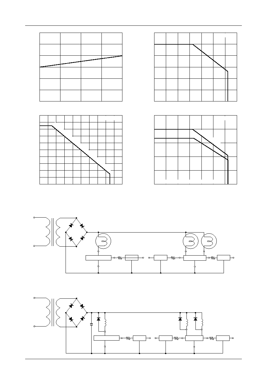
Sample Application Circuit
Another Sample Application Circuit
(solenoid drive)
--40
--20
0
20
40
60
80
100
0
0.5
1.0
1.5
1.7
2.0
2.5
Tj(sd) -- VIN
80
100
120
140
160
180
200
4.0
4.5
5.0
5.5
6.0
PD -- Ta
0
0.2
0.4
0.6
0.8
1.0
1.2
IT02024
--40
--20
0
20
40
60
80
100
PD -- Ta
IT02026
PD(Circuit 2) -- PD(Circuit 1)
0
0.2
0.4
0.6
0.8
1.0
1.2
1.4
1.6
1.8
2.0
0
0.2
0.4
0.6
0.8
1.0
1.2
1.4
1.6
1.8
2.0
IT02025
IT02023
1unit
TND017MP
TND017SW
TND017SW
Allowable Power Dissipation,
P
D
≠W
Ambient Temperature, Ta ≠ ∞C
Allowable Power Dissipation,
P
D
≠W
Allowable Power Dissipation,
P
D
(circuit 2)
≠
W
Ambient Temperature, Ta ≠ ∞C
Input Voltage, VIN ≠ V
Overheat detecting temperature,
Tj(sd)
≠
V
Mounted on a ceramic board (1200mm
2
◊
0.8mm)
Mounted on a ceramic board (1200mm
2
◊
0.8mm)
Total Dissipation
Allowable Power Dissipation, PD(circuit 1) ≠ W
AC100V
AC24V
OUT
IN
TND017MP / SW
5V 5V
IN 1
OUT 1
OUT 2
GND 1, 2
IN 2
5V
GND
TND017SW
Micro-
controller
Micro-
controller
Micro-
controller
Lamp
Lamp
Lamp
AC100V
AC24V
OUT
IN
TND017MP / SW
5V 5V
IN 1
OUT 1
OUT 2
GND 1, 2
IN 2
5V
GND
TND017SW
Micro-
controller
Micro-
controller
Micro-
controller
Solenoid
Solenoid
Solenoid

Specifications of any and all SANYO products described or contained herein stipulate the performance,
characteristics, and functions of the described products in the independent state, and are not guarantees
of the performance, characteristics, and functions of the described products as mounted in the customer's
products or equipment. To verify symptoms and states that cannot be evaluated in an independent device,
the customer should always evaluate and test devices mounted in the customer's products or equipment.
SANYO Electric Co., Ltd. strives to supply high-quality high-reliability products. However, any and all
semiconductor products fail with some probability. It is possible that these probabilistic failures could
give rise to accidents or events that could endanger human lives, that could give rise to smoke or fire,
or that could cause damage to other property. When designing equipment, adopt safety measures so
that these kinds of accidents or events cannot occur. Such measures include but are not limited to protective
circuits and error prevention circuits for safe design, redundant design, and structural design.
In the event that any or all SANYO products(including technical data,services) described or
contained herein are controlled under any of applicable local export control laws and regulations,
such products must not be expor ted without obtaining the expor t license from the author ities
concerned in accordance with the above law.
No part of this publication may be reproduced or transmitted in any form or by any means, electronic or
mechanical, including photocopying and recording, or any information storage or retrieval system,
or otherwise, without the prior written permission of SANYO Electric Co. , Ltd.
Any and all information described or contained herein are subject to change without notice due to
product/technology improvement, etc. When designing equipment, refer to the "Delivery Specification"
for the SANYO product that you intend to use.
Information (including circuit diagrams and circuit parameters) herein is for example only ; it is not
guaranteed for volume production. SANYO believes information herein is accurate and reliable, but
no guarantees are made or implied regarding its use or any infringements of intellectual property rights
or other rights of third parties.
This catalog provides information as of January, 2001. Specifications and information herein are subject
to change without notice.
TND017MP, 017SW
PS No.6481≠5/5
Operation Description
∑ The output power MOSFET will be turned on when the input voltage exceeds the input threshold voltage (4 to 6V
is recommended), and then the lamp will be turned on by the current flowing to the lamp. Conversely, the output
power MOSFET will be turned off when the input voltage goes below the input threshold voltage, and then the
lamp will be turned off.
∑ The inrush current that occurs during normal lamp operation is limited to a preset value by the built-in overcurrent
protecting circuit, which makes the lamp life longer.
∑ The internal overcurrent protection function limits the current of output power MOSFET when output current of at
least the overcurrent detecting current value flows at load short. Besides, if the device temperature exceeds the
allowable power dissipation, overheat protection function protects the power switch from being broken down by
shutting down the MOSFET when Tj comes to 150∞C (typical).
∑ Shutdown state will be kept after overheat protection operation and the system will be reset when the input voltage
goes to or below the reset voltage (1V).
∑ As an example of application circuit, DC voltage can also be controlled as a solenoid drive.