Semelab Plc reserves the right to change test conditions, parameter limits and package dimensions without notice. Information furnished by Semelab is believed
to be both accurate and reliable at the time of going to press. However Semelab assumes no responsibility for any errors or omissions discovered in its use.
Semelab encourages customers to verify that datasheets are current before placing orders.
Semelab plc.
Telephone +44(0)1455 556565. Fax +44(0)1455 552612.
E-mail:
sales@semelab.co.uk
Website:
http://www.semelab.co.uk
Document Number 3068
Issue 1
2N3637
PNP SILICON TRANSISTOR
FEATURES
∑ High Voltage Switching
∑ Low Power Amplifier Applications
∑ Hermetic TO39 Package
APPLICATIONS:
∑ General Purpose
∑ High Speed Saturated Switching
V
CEO
Collector ≠ Emitter Voltage
V
CBO
Collector ≠ Base Voltage
V
EBO
Emmiter ≠ Base Voltage
I
C
Collector Current
P
D
Total Device Dissipation @ T
A
= 25∞C
Derate above 25∞C
P
D
Total Device Dissipation @ T
C
= 25∞C
Derate above 25∞C
T
J
, T
STG
Operating and Storage Junction Temperature Range
-175V
-175V
-5V
-1A
1W
5.71mW/ ∞C
5W
28.6mW / ∞C
≠65 to +200∞C
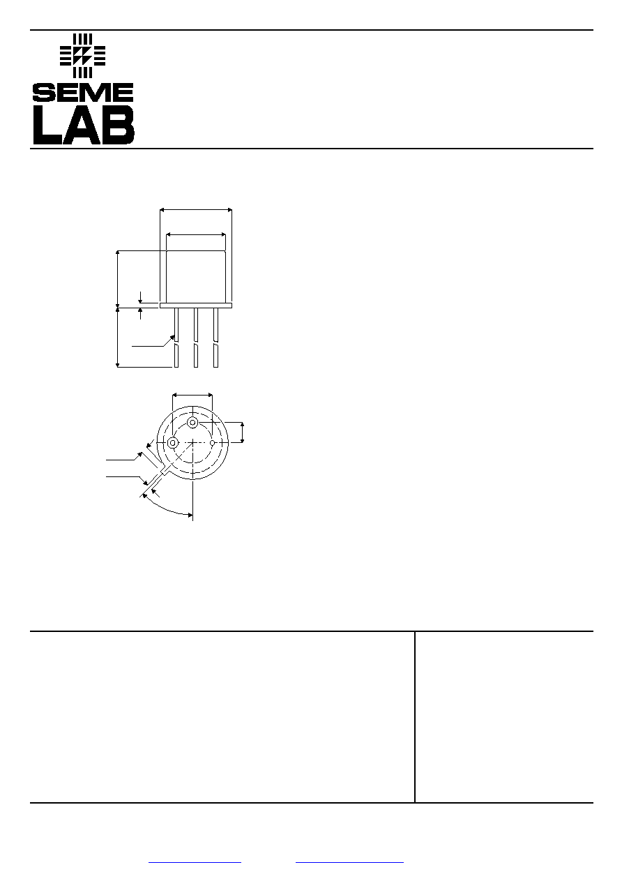
MECHANICAL DATA
Dimensions in mm (inches)
TO≠39 (TO-205AD) METAL PACKAGE
ABSOLUTE MAXIMUM RATINGS
(T
case
= 25∞C unless otherwise stated)
PIN 1 ≠ Emitter
Underside View
PIN 2 ≠ Base
PIN 3 ≠ Collector
0.89
(0.035)
max.
12.70
(0.500)
min.
0.41 (0.016)
0.53 (0.021)
dia.
5.08 (0.200)
typ.
0.71 (0.028)
0.86 (0.034)
2.54
(0.100)
45∞
6.10 (0.240)
6.60 (0.260)
8.51 (0.34)
9.40 (0.37)
7.75 (0.305)
8.51 (0.335)
1
2
3
0.74 (0.029)
1.14 (0.045)
Semelab Plc reserves the right to change test conditions, parameter limits and package dimensions without notice. Information furnished by Semelab is believed
to be both accurate and reliable at the time of going to press. However Semelab assumes no responsibility for any errors or omissions discovered in its use.
Semelab encourages customers to verify that datasheets are current before placing orders.
Parameter
Test Conditions
Min.
Typ.
Max.
Unit
-175
-175
-5.0
-50
-100
80
90
100
100
300
50
-0.3
-0.5
-0.8
-0.65
-0.9
200
10
75
200
1200
3.0
80
320
200
3.0
400
600
Semelab plc.
Telephone +44(0)1455 556565. Fax +44(0)1455 552612.
E-mail:
sales@semelab.co.uk
Website:
http://www.semelab.co.uk
BV
CEO
Collector≠Emitter Breakdown Voltage
1
BV
CBO
Collector ≠ Base Breakdown Voltage
BV
EBO
Emitter ≠ Base Breakdown Voltage
I
EBO
Emitter Cut-off Current
I
CBO
Collector Cut-off Current
h
FE
DC Current Gain
V
CE(sat)
Collector ≠ Emitter Saturation Voltage
1
V
BE(sat)
Base ≠ Emitter Saturation Voltage
f
t
Current Gain Bandwidth Product
C
ob
Output Capacitance
C
ib
Input Capacitance
h
ie
Input Impedance
h
re
Voltage Feedback Ratio
h
fe
Small Signal Current Gain
h
oe
Output Admittance
NF
Noise Figure
t
on
Turn≠On Time
t
off
Turn≠Off Time
I
C
= -10mA
I
B
= 0
I
C
= -100
µ
A
I
E
= 0
I
C
= 0
I
E
= -10
µ
A
V
BE
= -3.0V
I
C
= 0
V
CB
= -100V
I
E
= 0
I
C
= -0.1mA
V
CE
= -10V
I
C
= -1mA
V
CE
= -10V
I
C
= -10mA
V
CE
= -10V
I
C
= -50mA
V
CE
= -10V
I
C
= -150mA
V
CE
= -10V
I
C
= -10mA
I
B
= -1mA
I
C
= -50mA
I
B
= -5mA
I
C
= -10mA
I
B
= -1mA
I
C
= -50mA
I
B
= -5mA
V
CE
= -30V
I
C
= -30mA
f = 100MHz
V
CB
= -20V
I
E
= 0
f = 100kHz
V
BE
= 1.0V
I
C
= 0
f = 1MHz
V
CE
= -10V
I
C
= -10mA
f = 1kHz
V
CE
= -10V
I
C
= -0.5mA
R
S
= 1.0K
f = 1kHz
V
CC
= -100V
V
BE
= 4.0V
I
C
= -50mA I
B1
= I
B2
=-5mA
V
nA
-
V
V
MHz
pF
pF
x10
-4
--
µ
mhos
dB
ns
OFF CHARACTERISTICS
Document Number 3068
Issue 1
2N3637
ELECTRICAL CHARACTERISTICS
(T
A
= 25∞C unless otherwise stated)
1) Pulse test : Pulse Width < 300
µ
s ,Duty Cycle < 2%
ON CHARACTERISTICS
SWITCHING CHARACTERISTICS
SMALL SIGNAL CHARACTERISTICS