DESCRIPTION
The 2N5681 and 2N5682 are silicon
expitaxial planar NPN transistors in
jedec TO-39 metal case intended for
use as drivers for high power transis-
tors in general purpose, amplifier and
switching circuits
The complementary PNP types are the
2N5679 and 2N5680 respectively
ABSOLUTE MAXIMUM RATINGS
T
CASE
= 25∞c unless otherwise stated
2N5682
2N5681
2N5681
2N5682
Prelim.3/00
Semelab plc.
Telephone +44(0)1455 556565. Fax +44(0)1455 552612.
E-mail:
sales@semelab.co.uk
Website:
http://www.semelab.co.uk
NPN SILICON
TRANSISTORS
V
CBO
Collector ≠ Base Voltage(I
E
= 0)
V
CEO
Collector ≠ Emitter Voltage (I
B
= 0)
V
EBO
Emitter ≠ Base Voltage (I
C
= 0)
I
C
Continuous Collector Current
I
B
Base Current
P
tot
Total Dissipation at T
case
£
25∞C
T
amb
£
25∞C
T
stg
Operating and Storage Temperature Range
T
j
Junction temperature
100V
120V
100V
120V
4V
1A
0.5A
10W
1W
≠65 to +200∞C
200∞C
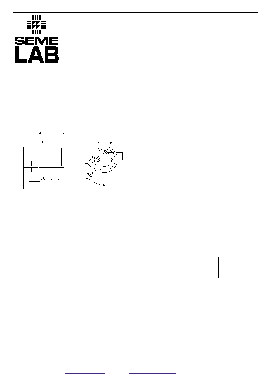
MECHANICAL DATA
Dimensions in mm (inches)
0 . 8 9
( 0 . 0 3 5 )
m a x .
1 2 . 7 0
( 0 . 5 0 0 )
m i n .
6 . 1 0 ( 0 . 2 4 0 )
6 . 6 0 ( 0 . 2 6 0 )
8 . 8 9 ( 0 . 3 5 )
9 . 4 0 ( 0 . 3 7 )
7 . 7 5 ( 0 . 3 0 5 )
8 . 5 1 ( 0 . 3 3 5 )
7 . 7 5 ( 0 . 3 0 5 )
8 . 5 1 ( 0 . 3 3 5 )
d i a .
0 . 6 6 ( 0 . 0 2 6 )
1 . 1 4 ( 0 . 0 4 5 )
0 . 7 1 ( 0 . 0 2 8 )
0 . 8 6 ( 0 . 0 3 4 )
2 . 5 4
( 0 . 1 0 0 )
5 . 0 8 ( 0 . 2 0 0 )
t y p .
4 5 ∞
!
TO-39
Pin 1 ≠ Emitter
Pin 2 ≠ Base
Pin 3 ≠ Collector
Parameter
Test Conditions
Min.
Typ.
Max.
Unit
µA
µA
mA
µA
V
MHz
pF
R
thj-case
R
thj-amb
17.5
175
Thermal Resistance Junction-case
Max
Thermal Resistance Junction-ambient
Max
∞C/W
∞C/W
1
1
1
1
1
1
10
10
1
100
120
0.6
1
2
1
40
150
5
30
50
40
2N5681
2N5682
Prelim.3/00
Semelab plc.
Telephone +44(0)1455 556565. Fax +44(0)1455 552612.
E-mail:
sales@semelab.co.uk
Website:
http://www.semelab.co.uk
I
CBO
I
CEV
I
CEO
I
EBO
V
CEO(sus)*
V
CE(sat)*
V
BE*
h
FE*
f
T
C
CBO
h
fe
Collector Cut Off Current
Collector Cut Off Current
Collector Cut Off Current
Emitter Cut Off Current
Collector Emitter Sustaining Voltage
Collector Emitter Saturation Voltage
Base Emitter Voltage
DC Current Gain
Transistion Frequency
Collector Base Capacitance
Small Signal Current Gain
I
E
= 0
for 2N5681
V
CB
= 100V
for 2N5682
V
CB
= 120V
V
BE
= -1.5
for 2N5681
V
CE
= 100V
for 2N5682
V
CE
= 120V
Tcase = 150∞C
for 2N5681
V
CE
= 100V
for 2n5682
V
CE
= 120V
I
B
= 0
for 2N5681
V
CE
= 70V
for 2N5682
V
CE
= 80V
I
C
= 0
V
EB
= 4V
I
B
= 0
I
C
= -10mA
for 2N5681
for 2N5682
I
C
= 250mA
I
B
= 25mA
I
C
= 500mA
I
B
= 50mA
I
C
= 1A
I
B
= 200mA
I
C
= 250mA
V
CE
= 2V
I
C
= 250mA
V
CE
= 2V
I
C
= 1A
V
CE
= 2V
I
C
= 100mA
V
CE
= 10V
f = 10MHz
I
E
= 0
V
CB
= 20V
f = 1MHz
I
C
= 0.2A
V
CE
= 1.5V
f = 1KHz
ELECTRICAL CHARACTERISTICS
(Tcase = 25∞C unless otherwise stated)
* Pulse test t
p
= 300
m
s ,
d
< 2%
THERMAL DATA