 | –≠–ª–µ–∫—Ç—Ä–æ–Ω–Ω—ã–π –∫–æ–º–ø–æ–Ω–µ–Ω—Ç: BCW33/T1 | –°–∫–∞—á–∞—Ç—å:  PDF PDF  ZIP ZIP |

DATA SHEET
Product specification
Supersedes data of September 1994
File under Discrete Semiconductors, SC04
1997 Jan 29
DISCRETE SEMICONDUCTORS
BCW31; BCW32; BCW33
NPN general purpose transistors
ok, halfpage
M3D088
1997 Jan 29
2
Philips Semiconductors
Product specification
NPN general purpose transistors
BCW31; BCW32; BCW33
FEATURES
∑
Low current (100 mA)
∑
Low voltage (32 V).
APPLICATIONS
∑
General purpose switching and amplification.
DESCRIPTION
NPN transistors in a plastic SOT23 package.
PNP complements: BCW29 and BCW30.
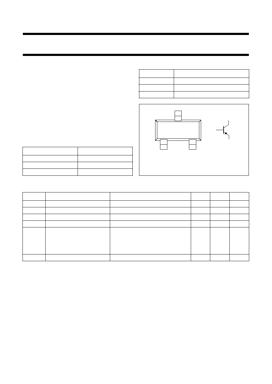
PINNING
PIN
DESCRIPTION
1
base
2
emitter
3
collector
Fig.1 Simplified outline (SOT23) and symbol.
handbook, halfpage
2
1
3
MAM255
Top view
2
3
1
MARKING
TYPE NUMBER
MARKING CODE
BCW31
D1p
BCW32
D2p
BCW33
D3p
QUICK REFERENCE DATA
SYMBOL
PARAMETER
CONDITIONS
MIN.
MAX.
UNIT
V
CBO
collector-base voltage
open emitter
-
32
V
V
CEO
collector-emitter voltage
open base
-
32
V
I
CM
peak collector current
-
200
mA
P
tot
total power dissipation
T
amb
25
∞
C
-
250
mW
h
FE
DC current gain
I
C
= 2 mA; V
CE
= 5 V
BCW31
110
220
BCW32
200
450
BCW33
420
800
f
T
transition frequency
I
C
= 10 mA; V
CE
= 5 V; f = 100 MHz
100
-
MHz

1997 Jan 29
3
Philips Semiconductors
Product specification
NPN general purpose transistors
BCW31; BCW32; BCW33
LIMITING VALUES
In accordance with the Absolute Maximum Rating System (IEC 134).
THERMAL CHARACTERISTICS
Note
1. Transistor mounted on an FR4 printed-circuit.
SYMBOL
PARAMETER
CONDITIONS
MIN.
MAX.
UNIT
V
CBO
collector-base voltage
open emitter
-
32
V
V
CEO
collector-emitter voltage
open base; I
C
= 2 mA
-
32
V
V
EBO
emitter-base voltage
open collector
-
5
V
I
C
collector current (DC)
-
100
mA
I
CM
peak collector current
-
200
mA
I
BM
peak base current
-
200
mA
P
tot
total power dissipation
T
amb
25
∞
C
-
250
mW
T
stg
storage temperature
-
65
+150
∞
C
T
j
junction temperature
-
150
∞
C
T
amb
operating ambient temperature
-
65
+150
∞
C
SYMBOL
PARAMETER
CONDITIONS
VALUE
UNIT
R
th j-a
thermal resistance from junction to ambient
note 1
500
K/W

1997 Jan 29
4
Philips Semiconductors
Product specification
NPN general purpose transistors
BCW31; BCW32; BCW33
CHARACTERISTICS
T
j
= 25
∞
C unless otherwise specified.
SYMBOL
PARAMETER
CONDITIONS
MIN.
TYP.
MAX.
UNIT
I
CBO
collector cut-off current
I
E
= 0; V
CB
= 32 V
-
-
100
nA
I
E
= 0; V
CB
= 32 V; T
j
= 100
∞
C
-
-
10
µ
A
I
EBO
emitter cut-off current
I
C
= 0; V
EB
= 5 V
-
-
100
nA
h
FE
DC current gain
I
C
= 10
µ
A; V
CE
= 5 V
BCW31
-
90
-
BCW32
-
150
-
BCW33
-
270
-
h
FE
DC current gain
I
C
= 2 mA; V
CE
= 5 V
BCW31
110
-
220
BCW32
200
-
450
BCW33
420
-
800
V
CEsat
collector-emitter saturation
voltage
I
C
= 10 mA; I
B
= 0.5 mA
-
120
250
mV
I
C
= 50 mA; I
B
= 2.5 mA
-
210
-
mV
V
BEsat
base-emitter saturation voltage
I
C
= 10 mA; I
B
= 0.5 mA
-
750
-
mV
I
C
= 50 mA; I
B
= 2.5 mA
-
850
-
mV
V
BE
base-emitter voltage
I
C
= 2 mA; V
CE
= 5 V
550
-
700
mV
C
c
collector capacitance
I
E
= I
e
= 0; V
CB
= 10 V; f = 1 MHz
-
2.5
-
pF
f
T
transition frequency
I
C
= 10 mA; V
CE
= 5 V; f = 100 MHz
100
-
-
MHz
F
noise figure
I
C
= 200
µ
A; V
CE
= 5 V; R
S
= 2 k
;
f = 1 kHz; B = 200 Hz
-
-
10
dB

1997 Jan 29
5
Philips Semiconductors
Product specification
NPN general purpose transistors
BCW31; BCW32; BCW33
PACKAGE OUTLINE
UNIT
A
1
max.
b
p
c
D
E
e
1
H
E
L
p
Q
w
v
REFERENCES
OUTLINE
VERSION
EUROPEAN
PROJECTION
ISSUE DATE
IEC
JEDEC
EIAJ
mm
0.1
0.48
0.38
0.15
0.09
3.0
2.8
1.4
1.2
0.95
e
1.9
2.5
2.1
0.55
0.45
0.1
0.2
DIMENSIONS (mm are the original dimensions)
0.45
0.15
SOT23
bp
D
e1
e
A
A1
Lp
Q
detail X
HE
E
w
M
v
M
A
B
A
B
0
1
2 mm
scale
A
1.1
0.9
c
X
1
2
3
Package description
SOT23