IRF044SMD
Prelim. 7/00
LAB
SEME
Semelab plc.
Telephone +44(0)1455 556565. Fax +44(0)1455 552612.
E-mail: sales@semelab.co.uk
Website: http://www.semelab.co.uk
V
GS
Gate ≠ Source Voltage
I
D
Continuous Drain Current
(V
GS
= 0 , T
case
= 25∞C)
I
D
Continuous Drain Current
(V
GS
= 0 , T
case
= 100∞C)
I
DM
Pulsed Drain Current
1
P
D
Power Dissipation @ T
case
= 25∞C
Linear Derating Factor
E
AS
Single Pulse Avalanche Energy
2
dv/dt
Peak Diode Recovery
3
T
J
, T
stg
Operating and Storage Temperature Range
T
L
Package Mounting Surface Temperature (for 5 sec)
R
q
JC
Thermal Resistance Junction to Case
R
q
J≠PCB
Thermal Resistance Junction to PCB (Typical)
±20V
34A
21A
136A
75W
0.6W/∞C
340mJ
4.5V/ns
≠55 to 150∞C
300∞C
1.67∞C/W
4∞C/W
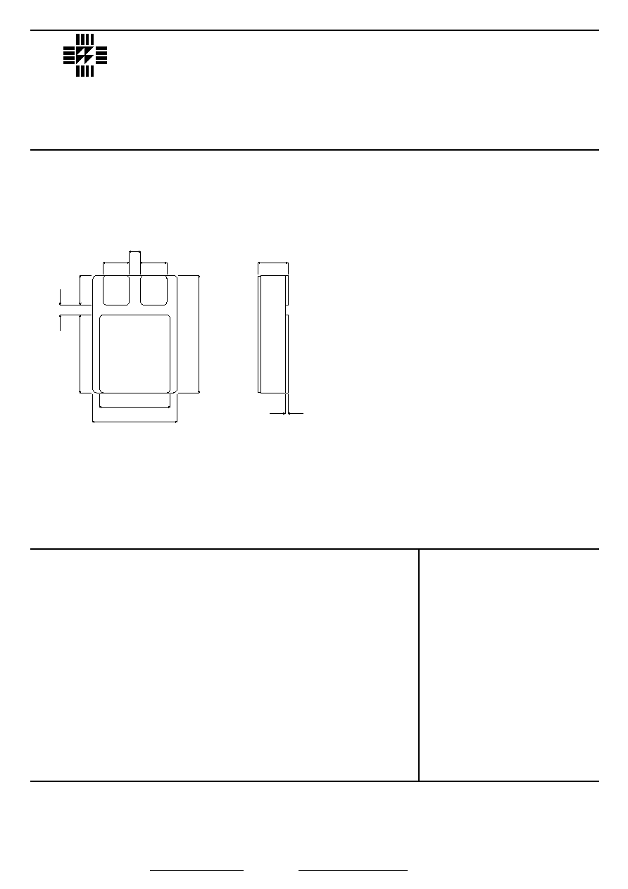
MECHANICAL DATA
Dimensions in mm (inches)
3 . 6 0 ( 0 . 1 4 2 )
M a x .
3 . 7 0 ( 0 . 1 4 6 )
3 . 4 1 ( 0 . 1 3 4 )
3 . 7 0 ( 0 . 1 4 6 )
3 . 4 1 ( 0 . 1 3 4 )
0 . 8 9
( 0 . 0 3 5 )
m i n .
4.
14
(
0.
163)
3.
84
(
0.
151)
10.
69
(
0
.
4
21)
10.
39
(
0
.
4
09)
9 . 6 7 ( 0 . 3 8 1 )
9 . 3 8 ( 0 . 3 6 9 )
1 1 . 5 8 ( 0 . 4 5 6 )
1 1 . 2 8 ( 0 . 4 4 4 )
16.
02
(
0
.
6
31)
15.
73
(
0
.
6
19)
0 . 5 0 ( 0 . 0 2 0 )
0 . 2 6 ( 0 . 0 1 0 )
0.
76
(
0
.
030) mi
n
.
1
3
2
N≠CHANNEL
POWER MOSFET
ABSOLUTE MAXIMUM RATINGS
(T
case
= 25∞C unless otherwise stated)
FEATURES
∑ HERMETICALLY SEALED SURFACE
MOUNT PACKAGE
∑ SMALL FOOTPRINT ≠ EFFICIENT USE OF
PCB SPACE.
∑ SIMPLE DRIVE REQUIREMENTS
∑ LIGHTWEIGHT
∑ HIGH PACKING DENSITIES
SMD1 ≠ Surface Mount Package
Pad 1 ≠ Gate
Pad 2 ≠ Drain
Pad 3 ≠ Source
Note:
IRFNxxx also available with
pins 1 and 3 reversed.
Notes
1) Pulse Test: Pulse Width
£
300ms,
d £
2%
2) @ V
DD
= 25V , L
≥
0.3mH , R
G
= 25
W
, Peak I
L
= 34A , Starting T
J
= 25∞C
3) @ I
SD
£
34A , di/dt
£
100A/
m
s , V
DD
£
BV
DSS
, T
J
£
150∞C , SUGGESTED R
G
= 9.1
W
V
DSS
60V
I
D(cont)
34A
R
DS(on)
0.040
W
W
W
W
IRF044SMD
Prelim. 7/00
LAB
SEME
Semelab plc.
Telephone +44(0)1455 556565. Fax +44(0)1455 552612.
E-mail: sales@semelab.co.uk
Website: http://www.semelab.co.uk
Parameter
Test Conditions
Min.
Typ.
Max.
Unit
V
GS
= 0
I
D
= 1mA
Reference to 25∞C
I
D
= 1mA
V
GS
= 10V
I
D
= 21A
V
GS
= 10V
I
D
= 34A
V
DS
= V
GS
I
D
= 250
m
A
V
DS
≥
15V
I
DS
= 21A
V
GS
= 0
V
DS
= 0.8BV
DSS
T
J
= 125∞C
V
GS
= 20V
V
GS
= ≠20V
V
GS
= 0
V
DS
= 25V
f = 1MHz
V
GS
= 10V
I
D
= 34A
V
DS
= 0.5BV
DSS
I
D
= 34A
V
DS
= 0.5BV
DSS
V
DD
= 30V
I
D
= 34A
R
G
= 9.1
W
I
S
= 34A
T
J
= 25∞C
V
GS
= 0
I
F
= 34A
T
J
= 25∞C
d
i
/ d
t
£
100A/
m
s V
DD
£
50V
ELECTRICAL CHARACTERISTICS
(Tamb = 25∞C unless otherwise stated)
Drain ≠ Source Breakdown Voltage
Temperature Coefficient of
Breakdown Voltage
Static Drain ≠ Source On≠State
Resistance
1
Gate Threshold Voltage
Forward Transconductance
1
Zero Gate Voltage Drain Current
Forward Gate ≠ Source Leakage
Reverse Gate ≠ Source Leakage
Input Capacitance
Output Capacitance
Reverse Transfer Capacitance
Total Gate Charge
1
Gate ≠ Source Charge
1
Gate ≠ Drain ("Miller") Charge
1
Turn≠On Delay Time
Rise Time
Turn≠Off Delay Time
Fall Time
Continuous Source Current
Pulse Source Current
2
Diode Forward Voltage
Reverse Recovery Time
Reverse Recovery Charge
Forward Turn≠On Time
60
0.68
0.040
0.050
2
4
17
25
250
100
≠100
2400
1100
230
39
88
6.7
15
18
52
23
130
81
79
34
136
2.5
220
1.6
Negligible
0.8
2.8
V
V / ∞C
W
V
S
(
W
m
A
nA
pF
nC
nC
ns
A
V
ns
m
C
nH
BV
DSS
D
BV
DSS
D
T
J
R
DS(on)
V
GS(th)
g
fs
I
DSS
I
GSS
I
GSS
C
iss
C
oss
C
rss
Q
g
Q
gs
Q
gd
t
d(on)
t
r
t
d(off)
t
f
I
S
I
SM
V
SD
t
rr
Q
rr
t
on
L
D
L
S
STATIC ELECTRICAL RATINGS
Notes
1) Pulse Test: Pulse Width
£
300ms,
d £
2%
2) Repetitive Rating ≠ Pulse width limited by maximum junction temperature.
DYNAMIC CHARACTERISTICS
SOURCE ≠ DRAIN DIODE CHARACTERISTICS
Internal Drain Inductance
(from centre of drain pad to die)
Internal Source Inductance
(from centre of source pad to end of source bond wire)
PACKAGE CHARACTERISTICS
(
W
)