Document Number 4145
Issue 1
IRFM240
2N7219
Semelab plc.
Telephone +44(0)1455 556565. Fax +44(0)1455 552612.
E-mail:
sales@semelab.co.uk
Website:
http://www.semelab.co.uk
Semelab Plc reserves the right to change test conditions, parameter limits and package dimensions without notice. Information furnished by Semelab is believed
to be both accurate and reliable at the time of going to press. However Semelab assumes no responsibility for any errors or omissions discovered in its use.
Semelab encourages customers to verify that datasheets are current before placing orders.
V
GS
Gate ≠ Source Voltage
I
D
Continuous Drain Current
@ V
GS
= 10V , T
C
= 25∞C
@ V
GS
= 10V , T
C
= 100∞C
I
DM
Pulsed Drain Current
P
D
Max. Power Dissipation
@ T
C
= 25∞C
Linear Derating Factor
I
AR
Avalanche Current
1
dv / dt
Peak Diode Recovery
2
R
JC
Thermal Resistance Junction ≠ Case
R
JA
Thermal Resistance Junction ≠ Ambient
T
J
, T
STG
Operating Junction and Storage Temperature Range
T
L
Lead Temperature (1.6mm from case for 10s)
±20V
18A
11A
72A
125W
1.0W / ∞C
18
5.0V / ns
1.0∞C / W
48∞C / W
≠55 to 150∞C
300∞C
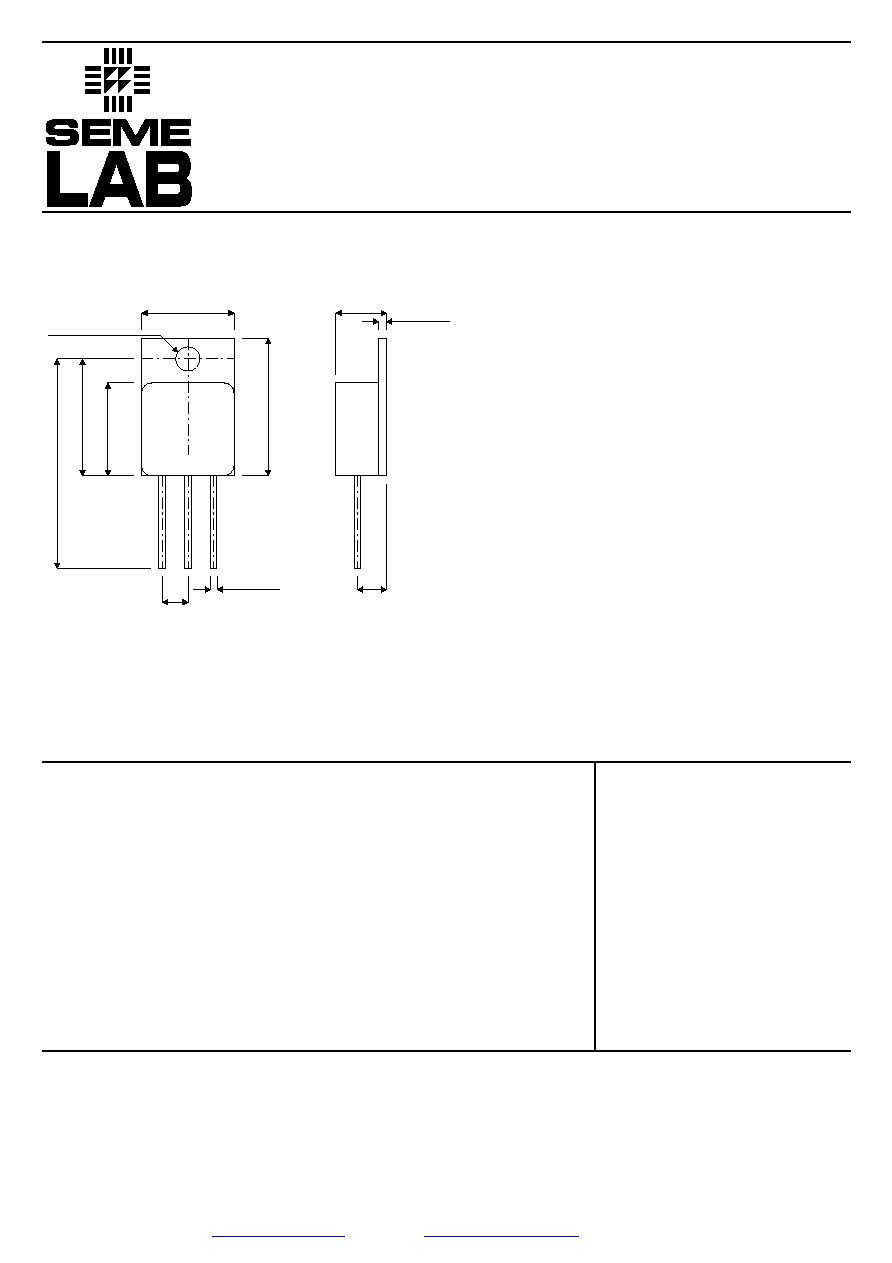
MECHANICAL DATA
Dimensions in mm (inches)
1
2
3
13.59 (0.535)
13.84 (0.545)
3.53 (0.139)
3.78 (0.149)
Dia.
6.32 (0.249)
6.60 (0.260)
1.02 (0.040)
1.27 (0.050)
30.
35 (
1
.
195)
31.
40 (
1
.
235)
16.
89 (
0
.
665)
17.
40 (
0
.
685)
13.
59 (
0
.
5
35)
13.
84 (
0
.
5
45)
2
0
.
07 (0.
790)
2
0
.
32 (0.
800)
3.81 (0.150)
BSC
0.89 (0.035)
1.14 (0.045)
3.81 (0.150)
BSC
TO≠254AA ≠ Isolated Metal Package
Pin 1 ≠ Drain
Pin 2 ≠ Source
Pin 3 ≠ Gate
ABSOLUTE MAXIMUM RATINGS
(T
C
= 25∞C unless otherwise stated)
1)
V
DD
= 50V , Starting T
J
= 25∞C , L
1.3mH , V
GS
= 10V , Peak I
L
= 18A
2)
I
SD
18A , di/dt
150A /
µ
S , V
DD
200V , T
J
150∞C
N≠CHANNEL
POWER MOSFET
FEATURES
∑ N≠CHANNEL MOSFET
∑ HIGH VOLTAGE
∑ HERMETIC ISOLATED TO-254 PACKAGE
∑ ELECTRICALLY ISOLATED
V
DSS
200V
I
D(cont)
18A
R
DS(on)
0.18
Document Number 4145
Issue 1
IRFM240
2N7219
Semelab plc.
Telephone +44(0)1455 556565. Fax +44(0)1455 552612.
E-mail:
sales@semelab.co.uk
Website:
http://www.semelab.co.uk
Semelab Plc reserves the right to change test conditions, parameter limits and package dimensions without notice. Information furnished by Semelab is believed
to be both accurate and reliable at the time of going to press. However Semelab assumes no responsibility for any errors or omissions discovered in its use.
Semelab encourages customers to verify that datasheets are current before placing orders.
Parameter
Test Conditions
Min.
Typ.
Max.
Unit
V
GS
= 0
I
D
= 1mA
Reference to 25∞C
I
D
= 1mA
V
GS
= 10V
I
D
= 11A
V
GS
= 10V
I
D
= 18A
V
DS
= V
GS
I
D
= 250
µ
A
V
DS
15V
I
DS
= 11A
V
GS
= 0
V
DS
= 160V
T
J
= 125∞C
V
GS
= 20V
V
GS
= ≠20V
V
GS
= 0
V
DS
= 25V
f = 1MHz
V
GS
= 10V
I
D
= 18A
V
DS
= 100V
V
DD
= 100V
I
D
= 18A
V
GS
= 10V
R
G
= 9.1
I
S
= 18A
T
J
= 25∞C
V
GS
= 0
I
F
= 18A
T
J
= 25∞C
d
i
/ d
t
100A/
µ
s V
DD
50V
ELECTRICAL CHARACTERISTICS
(T
J
= 25∞C unless otherwise stated)
Drain ≠ Source Breakdown Voltage
Temperature Coefficient of
Breakdown Voltage
Static Drain ≠ Source On≠State
Resistance
2
Gate Threshold Voltage
Forward Transconductance
2
Zero Gate Voltage Drain Current
Forward Gate ≠ Source Leakage
Reverse Gate ≠ Source Leakage
Input Capacitance
Output Capacitance
Reverse Transfer Capacitance
Total Gate Charge
Gate ≠ Source Charge
Gate ≠ Drain ("Miller") Charge
Turn≠ On Delay Time
Rise Time
Turn≠Off Delay Time
Fall Time
Continuous Source Current
Pulse Source Current
1
Diode Forward Voltage
2
Reverse Recovery Time
2
Reverse Recovery Charge
2
Forward Turn≠On Time
200
0.29
0.18
0.25
2.0
4.0
6.1
25
250
100
≠100
1300
400
130
60
10.6
37.6
20
105
58
67
18
72
1.5
500
5.3
Negligible
4.0
4.0
V
V / ∞C
V
S
(
µ
A
nA
pF
nC
ns
A
V
ns
µ
C
nH
BV
DSS
BV
DSS
T
J
R
DS(on)
V
GS(th)
g
fs
I
DSS
I
GSS
I
GSS
C
iss
C
oss
C
rss
Q
g
Q
gs
Q
gd
t
d(on)
t
r
t
d(off)
t
f
I
S
I
SM
V
SD
t
rr
Q
rr
t
on
L
D
L
S
STATIC ELECTRICAL RATINGS
1) Repetitive Rating ≠ Pulse width limited by Maximum Junction Temperature
2) Pulse Test: Pulse Width
300
µ
s,
2%.
DYNAMIC CHARACTERISTICS
SOURCE ≠ DRAIN DIODE CHARACTERISTICS
Internal Drain Inductance
Measured from drain lead (6mm / 0.25in from package) to
Internal Source Inductance
source lead (6mm / 0.25in from package).
PACKAGE CHARACTERISTICS
(
)