IRFM5210
Document Number 2612
Issue 1
Semelab plc.
Telephone +44(0)1455 556565. Fax +44(0)1455 552612.
E-mail:
sales@semelab.co.uk
Website:
http://www.semelab.co.uk
Semelab Plc reserves the right to change test conditions, parameter limits and package dimensions without notice. Information furnished by Semelab is believed
to be both accurate and reliable at the time of going to press. However Semelab assumes no responsibility for any errors or omissions discovered in its use.
Semelab encourages customers to verify that datasheets are current before placing orders.
1
2
3
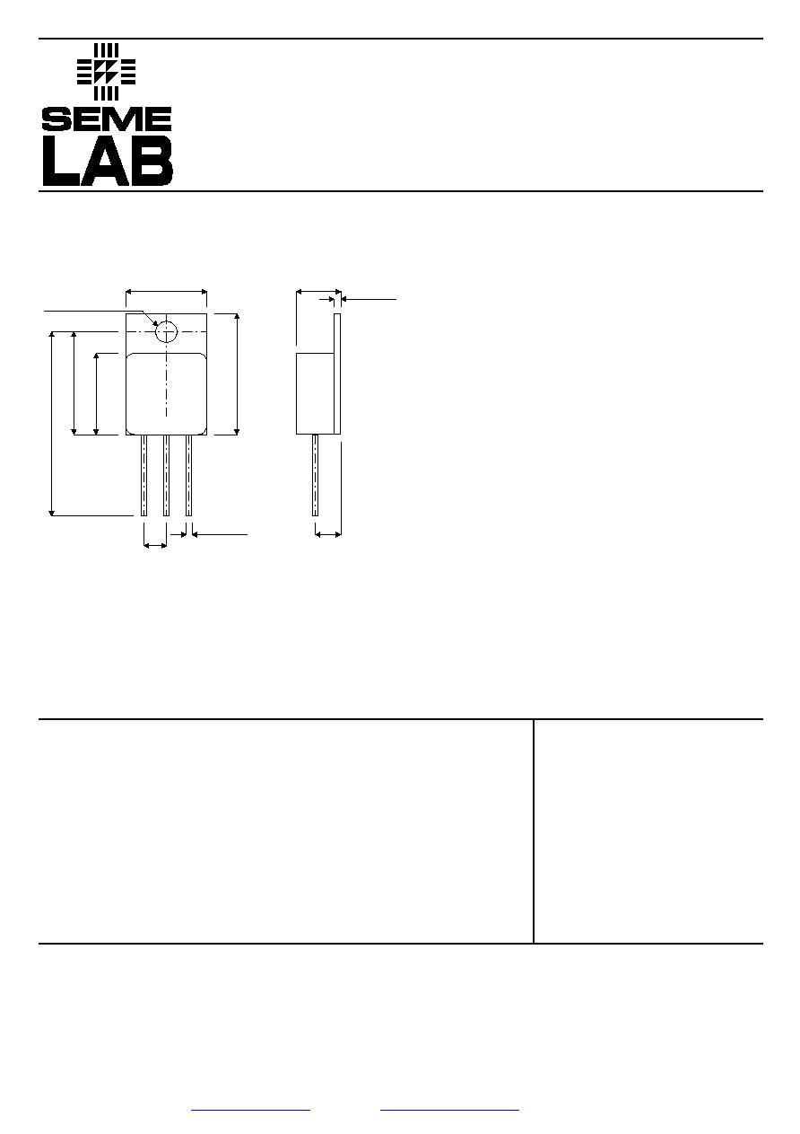
13.59 (0.535)
13.84 (0.545)
3.53 (0.139)
3.78 (0.149)
Dia.
6.32 (0.249)
6.60 (0.260)
1.02 (0.040)
1.27 (0.050)
30.
35 (
1
.
195)
31.
40 (
1
.
235)
16.
89 (
0
.
665)
17.
40 (
0
.
685)
13.
59 (
0
.
5
35)
13.
84 (
0
.
5
45)
2
0
.
07 (0.
790)
2
0
.
32 (0.
800)
3.81 (0.150)
BSC
0.89 (0.035)
1.14 (0.045)
3.81 (0.150)
BSC
V
GS
Gate ≠ Source Voltage
I
D
Continuous Drain Current
(T
case
= 25∞C)
I
D
Continuous Drain Current
(T
case
= 100∞C)
I
DM
Pulsed Drain Current
1
P
D
Power Dissipation
Linear Derating Factor
E
AS
Single Pulse Avalanche Energy
2
E
AR
Repetitive Avalanche Energy
1
T
J
, T
stg
Operating Junction and Storage Temperature Range
R
JC
Junction ≠ Case Thermal Resistance
MECHANICAL DATA
Dimensions in mm (inches)
P≠CHANNEL MOSFET
IN A TO254
FOR HIGH RELIABILITY
APPLICATIONS.
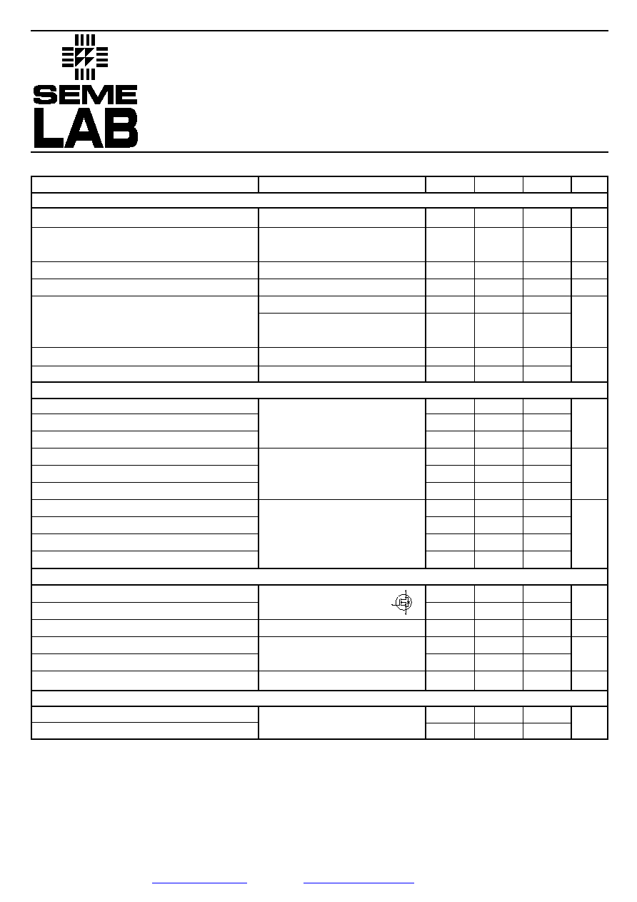
ABSOLUTE MAXIMUM RATINGS
(T
case
= 25∞C unless otherwise stated)
FEATURES
∑ FAST SWITCHING
∑ SCREENING OPTIONS AVAILABLE
TO-254AA
Pin 1 ≠Drain
Pin 2 ≠ Source
Pin 3 ≠ Gate
Notes
1) Repetitive rating; pulse width limited by max. junction temperature.
2) V
DD
= ≠25V , L = 3.5mH , R
G
= 25
, I
AS
= ≠21A , Starting T
J
= 25∞C, V
GS
= ≠10V
V
DSS
100V
I
D
34A
R
DS(on)
0.07
±20V
-34A
-21A
-136A
125W
1.0W/∞C
520mJ
12mJ
≠55 to +150∞C
1.0W/∞C
IRFM5210
Document Number 2612
Issue 1
Semelab plc.
Telephone +44(0)1455 556565. Fax +44(0)1455 552612.
E-mail:
sales@semelab.co.uk
Website:
http://www.semelab.co.uk
Semelab Plc reserves the right to change test conditions, parameter limits and package dimensions without notice. Information furnished by Semelab is believed
to be both accurate and reliable at the time of going to press. However Semelab assumes no responsibility for any errors or omissions discovered in its use.
Semelab encourages customers to verify that datasheets are current before placing orders.
Parameter
Test Conditions
Min.
Typ.
Max.
Unit
≠100
0.07
≠ 2.0
≠4.0
10
≠25
≠250
≠100
100
2700
790
450
180
25
97
17
28
86
150
79
100
81
120
100
≠34
≠136
≠1.6
170
260
1.2
1.8
5.0
17
4.5
7.5
V
GS
= 0V
I
D
= ≠250
µ
A
V
GS
= ≠10V
I
D
= ≠21A
V
DS
= V
GS
I
D
= ≠250
µ
A
V
DS
= ≠15V
I
D
= ≠21A
V
DS
= ≠100V
V
GS
= 0V
V
DS
= ≠80V
V
GS
= 0V
T
J
= 125∞C
V
GS
= ≠20V
V
GS
= 20V
V
GS
= 0V
V
DS
= ≠25V
f = 1MHz
I
D
= ≠21A
V
DS
= ≠80V
V
GS
= ≠10V
V
DD
= ≠50V
I
D
= ≠21A
R
G
= 2.5
V
GS
= ≠10V
R
G
= 2.4
MOSFET symbol showing the
integral reverse p-n junction
T
J
= 25∞C, I
S
= 21A, V
GS
= 0V
d
i
/ d
t
≠100A/
µ
s
T
J
= 25∞C, I
F
= -21A
negligible
Between lead, 6mm(0.25in.) from
package and center of die contact
ELECTRICAL CHARACTERISTICS
(Tcase = 25∞C unless otherwise stated)
Drain ≠ Source Breakdown Voltage
Static Drain to Source On
Resistance 2
Gate Threshold Voltage
Forward Transconductance
Drain to Source Leakage Current
Gate to Source Forward Leakage
Gate to Source Reverse Leakage
Input Capacitance
Output Capacitance
Reverse Transfer Capacitance
Total Gate Charge
Gate ≠ Source Charge
Gate ≠ Drain ("Miller") Charge
Turn≠On Delay Time
Rise Time
Turn≠Off Delay Time
Fall Time
Continuous Source Current
Pulse Source Current
1
Diode Forward Voltage
2
Reverse Recovery Time
2
Reverse Recovery Charge
2
Forward Turn≠On Time
Internal Drain
Internal Source Inductance
V
V
S
µ
A
nA
pF
nC
ns
A
V
ns
µ
C
--
nH
V
(BR)DSS
R
DS(on)
V
GS(th)
g
fs
I
DSS
I
GSS
I
GSS
C
iss
C
oss
C
rss
Q
g
Q
gs
Q
gd
t
d(on)
t
r
t
d(off)
t
f
I
S
I
SM
V
SD
t
rr
Q
rr
t
on
L
D
L
S
STATIC ELECTRICAL RATINGS
Notes
1) Repetitive rating; pulse width limited by max. junction temperature.
2) Pulse Test: Pulse Width
300ms,
2%
DYNAMIC CHARACTERISTICS
SOURCE ≠ DRAIN CHARACTERISTICS
PACKAGE CHARACTERISTICS
D
S
G