IRFY9140C
Semelab plc.
Telephone (01455) 556565. Telex: 341927. Fax (01455) 552612.
Prelim. 9/95
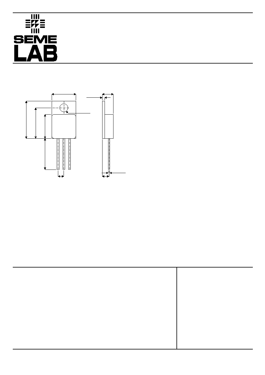
MECHANICAL DATA
Dimensions in mm (inches)
P≠CHANNEL
POWER MOSFET
FOR HI≠REL
APPLICATIONS
V
DSS
-100V
I
D(cont)
-12A
R
DS(on)
0.21
V
GS
Gate ≠ Source Voltage
I
D
Continuous Drain Current @ T
case
= 25∞C
I
D
Continuous Drain Current @ T
case
= 100∞C
I
DM
Pulsed Drain Current
P
D
Power Dissipation @ T
case
= 25∞C
Linear Derating Factor
T
J
, T
stg
Operating and Storage Temperature Range
R
JC
Thermal Resistance Junction to Case
R
JA
Thermal Resistance Junction to Ambient
±20V
-12A
-8A
-48A
60W
0.48W/∞C
≠55 to 150∞C
2.1∞C/W max.
80∞C/W max.
ABSOLUTE MAXIMUM RATINGS
(T
case
= 25∞C unless otherwise stated)
1 2 3
0.89 (0.035)
1.14 (0.045)
10.41 (0.410)
10.67 (0.420)
3.56 (0.140)
3.81 (0.150)
4.83 (0.190)
5.08 (0.200)
10.
41 (
0
.
4
1
0
)
10.
92 (
0
.
4
3
0
)
13.
3
8
(
0
.
527
)
13.
6
4
(
0
.
537
)
1
6
.
3
8 (
0
.
645)
1
6
.
8
9 (
0
.
665)
0.64 (0.025)
0.89 (0.035)
3.05 (0.120)
BSC
2.54 (0.100)
BSC
Dia.
1
2
.
0
7 (
0
.
500)
1
9
.
0
5 (
0
.
750)
Dia.
TO≠257AA ≠ Metal Package
FEATURES
∑ HERMETICALLY SEALED TO≠257AA
METAL PACKAGE
∑ SIMPLE DRIVE REQUIREMENTS
∑ LIGHTWEIGHT
∑ SCREENING OPTIONS AVAILABLE
∑ ALL LEADS ISOLATED FROM CASE
Pad 1 ≠ Gate
Pad 2 ≠ Drain
Pad 3 ≠ Source
IRFY9140C
Semelab plc.
Telephone (01455) 556565. Telex: 341927. Fax (01455) 552612.
Prelim. 9/95
Parameter
Test Conditions
Min.
Typ.
Max.
Unit
V
GS
= 0
I
D
= 1mA
Reference to 25∞C
I
D
= 1mA
V
GS
= 10V
I
D
= -8.2A
V
GS
= 10V
I
D
= -12A
V
DS
= V
GS
I
D
= 250
µ
A
V
DS
15V
I
DS
= -8.2A
V
GS
= 0
V
DS
= 0.8BV
DSS
T
J
= 125∞C
V
GS
= 20V
V
GS
= ≠20V
V
GS
= 0
V
DS
= 25V
f = 1MHz
V
GS
= 10V
I
D
= -12A
V
DS
= 0.5BV
DSS
I
D
= -12A
V
DS
= 0.5BV
DSS
V
DD
= -50V
I
D
= -12A
R
G
= 9.1
I
S
= -12A
T
J
= 25∞C
V
GS
= 0
I
S
= -12A
T
J
= 25∞C
d
i
/ d
t
100A/
µ
s V
DD
50V
ELECTRICAL CHARACTERISTICS
(T
C
= 25∞C unless otherwise stated)
Drain ≠ Source Breakdown Voltage
Temperature Coefficient of
Breakdown Voltage
Static Drain ≠ Source On≠State
Resistance
Gate Threshold Voltage
Forward Transconductance
Zero Gate Voltage Drain Current
Forward Gate ≠ Source Leakage
Reverse Gate ≠ Source Leakage
Input Capacitance
Output Capacitance
Reverse Transfer Capacitance
Total Gate Charge
Gate ≠ Source Charge
Gate ≠ Drain ("Miller") Charge
Turn≠On Delay Time
Rise Time
Turn≠Off Delay Time
Fall Time
Continuous Source Current
Pulse Source Current
Diode Forward Voltage
Reverse Recovery Time
Reverse Recovery Charge
-100
-0.09
0.21
0.24
-2
-4
6.2
25
250
100
-100
1400
600
200
31
60
3.7
13
7
35.2
35
85
85
65
-12
-48
-4.2
280
3.6
8.7
8.7
V
V / ∞C
V
S
(
µ
A
nA
pF
nC
nC
ns
A
V
ns
µ
C
nH
BV
DSS
BV
DSS
T
J
R
DS(on)
V
GS(th)
g
fs
I
DSS
I
GSS
I
GSS
C
iss
C
oss
C
rss
Q
g
Q
gs
Q
gd
t
d(on)
t
r
t
d(off)
t
f
I
S
I
SM
V
SD
t
rr
Q
rr
L
D
L
S
STATIC ELECTRICAL RATINGS
DYNAMIC CHARACTERISTICS
SOURCE ≠ DRAIN DIODE CHARACTERISTICS
Internal Drain Inductance
(from 6mm down drain lead pad to centre of die)
Internal Source Inductance
(from 6mm down source lead to centre of source bond pad)
PACKAGE CHARACTERISTICS
(
)