Internally Limited
35V
-55∞C to + 150∞C
-65∞C to + 150∞C
300∞C
2.75∞C/W
2.3∞C/W
5.0A
LT1084HN
02/00
Semelab plc.
Telephone +44(0)1455 556565. Fax +44(0)1455 552612.
E-mail:
sales@semelab.co.uk
Website:
http://www.semelab.co.uk
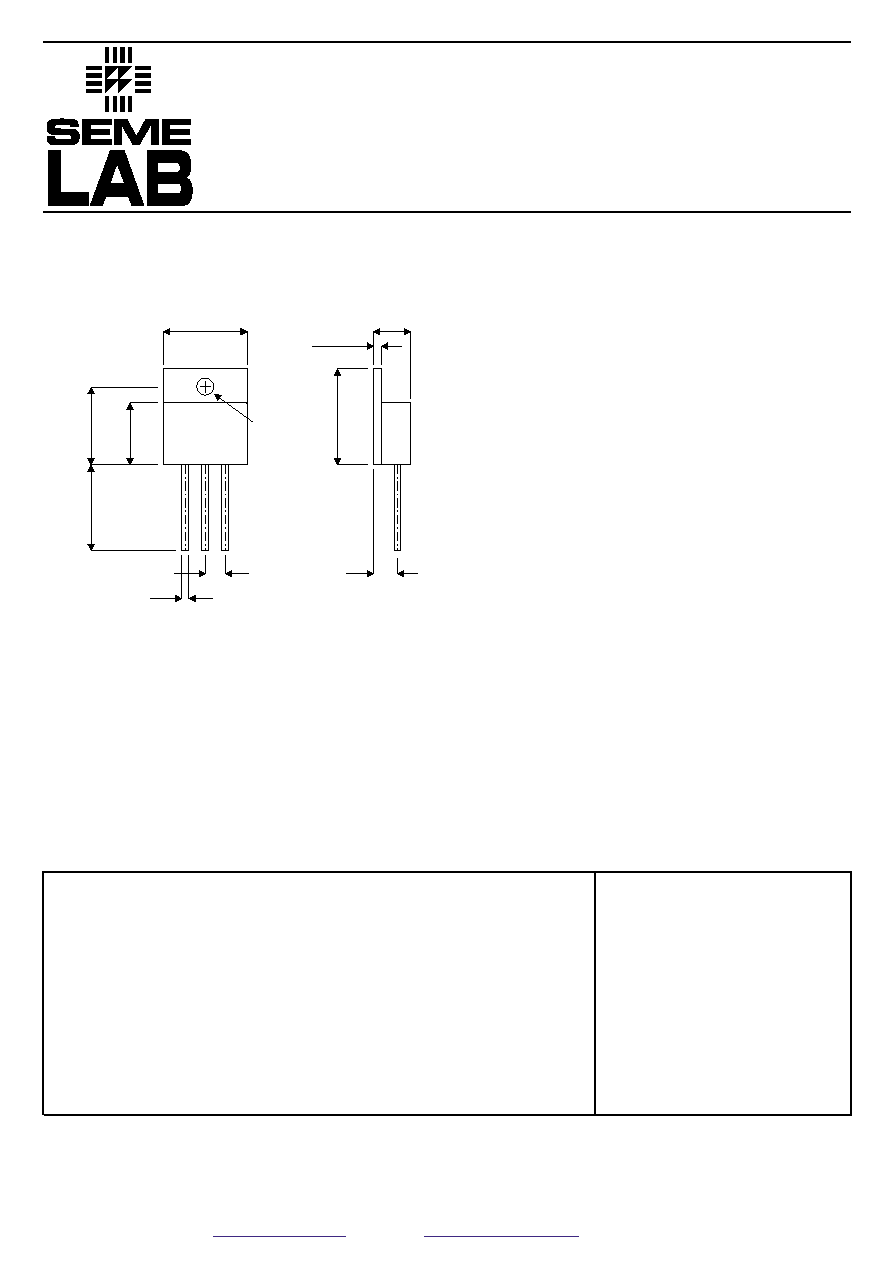
MECHANICAL DATA
Dimensions in mm
1
2
3
17.65 (0.695)
17.39 (0.685)
4.19 (0.165)
3.94 (0.155)
Dia.
13.
8
4
(
0
.
545
)
13.
5
8
(
0
.
535
)
1
7
.
9
6 (
0
.
7
07)
1
7
.
7
0 (
0
.
6
97)
19.
05 (
0
.
750
)
12.
70 (
0
.
500
)
1.65 (0.065)
1.39 (0.055)
Typ.
5.08 (0.200)
BSC
3.56 (0.140)
BSC
21
.
21 (
0
.
8
3
5
)
20
.
70 (
0
.
8
1
5
)
1.14 (0.707)
0.88 (0.035)
6.86 (0.270)
6.09 (0.240)
5 AMP LOW DROPOUT POSITIVE
ADJUSTABLE REGULATOR IN
TO258 HERMETIC PACKAGE
FEATURES
∑ Ajustable Output Voltage
∑ Output Voltage Tolerance ±1%
∑ Hermetic Isolated TO258
∑ Built in Thermal Overload Protection
∑ Short Circuit Current Limit
∑ Low Dropout Voltage
∑ Screening Options Available
TO≠258 METAL PACKAGE
ABSOLUTE MAXIMUM RATINGS
@25∞C
Pin 1≠ Adjust
Pin 2 ≠ Vout
Pin 3 ≠ Vin
Power Dissipation (Pd)
Input - Output Voltage Differential
Operating Junction Temperature Range
Storage Temperature Range
Lead Temperature (Soldering 10 seconds)
Thermal Resistance:
q
jc (Isolated)
q
jc (Non-Isolated)
Maximum Output Current
The LT1084HN low drop positive adjustable
regulator is designed to provide 5A with
higher efficiency than a standard device. All
internal circuitry is designed to operate
down to 1V input/output differential.

Parameter
Test Conditions
Min.
Typ.
Max.
Unit
1.238
1.262
1.225
1.270
0.2
0.5
0.3
0.4
1.5
0.015
60
120
5.0
10
5.5
0.3
1.5
1.0
LT1084HN
02/00
Semelab plc.
Telephone +44(0)1455 556565. Fax +44(0)1455 552612.
E-mail:
sales@semelab.co.uk
Website:
http://www.semelab.co.uk
V
REF
Reference Voltage
V
OUT
Line Regulation (Note 1)
V
IN
V
OUT
Load Regulation
V
IN
V
DO
Dropout Voltage
Thermal Regulation
V
IN
Ripple Rejection
V
OUT
I
Adj
Ajust Pin Current
3
I
Adj
Ajust Pin Current Change
I
Min
Minimum Load Current
I
Lim
Current Limit
V
OUT
Temperature Stability (Note 2)
T
V
OUT
Long Term Stability (Note 2)
T
V
IN
- V
OUT
=3.0V
I
OUT
= 10mA
T
A
= 25∞C
1.5V
£
V
IN
- V
OUT
£
25V
10mA
£
I
OUT
£
I
FL
1.5
£
V
IN
- V
OUT
£
15V
I
OUT
= 10mA
T
A
= 25∞C
15V
£
V
IN
- V
OUT
£
35V
I
OUT
=10mA
V
IN
- V
OUT
=3.0V
T
A
= 25∞C
10mA
£
I
OUT
£
I
FL
I
OUT
= I
FL
D
V
REF
= 1%
30ms pulse
T
A
= +25∞C
f = 120H
z,
C
Adj
= 25
m
F
C
OUT
= 25
m
F (tantalum), I
FL
= 3.0A
V
IN
- V
OUT
=3.0V
1.5V
£
V
IN
- V
OUT
£
25V
10mA
£
I
OUT
£
I
FL
1.5V
£
V
IN
- V
OUT
£
25V
10mA
£
I
OUT
£
I
FL
V
IN
- V
OUT
= 25V
V
IN
- V
OUT
= 5.0V
V
IN
- V
OUT
= 25V
Tj = -55 to +125∞C
T
A
= +125∞C, t = 1000hrs
V
%
%
V
%W
dB
m
A
m
A
mA
A
%
ELECTRICAL CHARACTERISTICS
(Per Diode)
∑
∑
∑
∑
∑
∑
∑
∑
∑
∑
∑
Notes:
1 Line and Load Regulation are measured at a constant junction temperature using a low duty cycle pulse technique.
Power dissipation is internally limted. Regulation is guaranteed up to maximum power dissipation of 45 W. Power
dissipation is determined by the input/output differential voltage and the output current. Guaranteed maximum power
dissipation is not available over the full input/output voltage range.
2 Guaranteed by design, characterization or correlation to other tested parameters.
3
∑
Specification applies over the full operating temperature range.
4 I
FL
is defined as the minimum value of current limit as a function of input to output voltage.