Prelim. 10/95
LT1085≠220M
≠05
LT1085≠05≠220M
LT1085≠12≠220M
MILITARY VERSION
Semelab plc.
Telephone +44(0)1455 556565. Fax +44(0)1455 552612.
E-mail:
sales@semelab.co.uk
Website:
http://www.semelab.co.uk
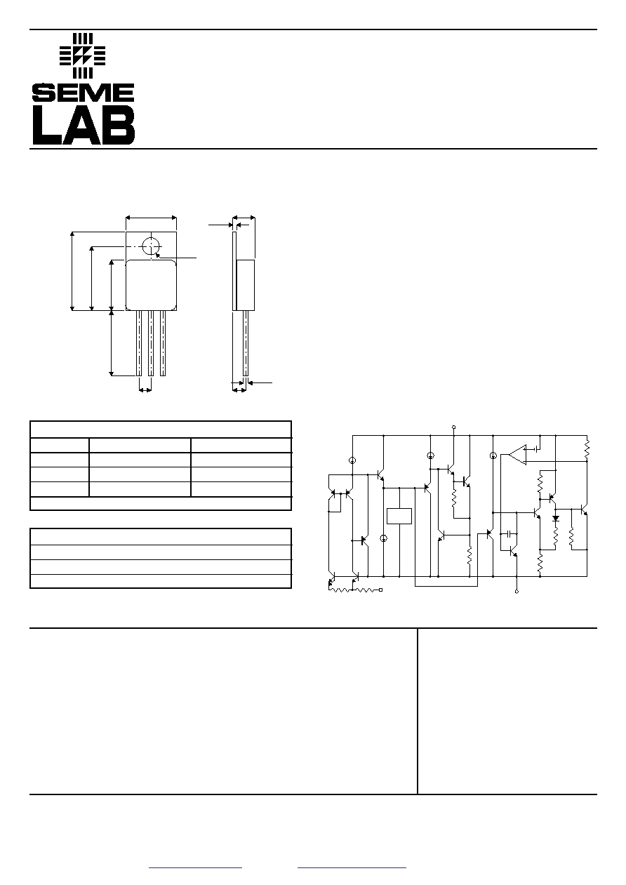
Dia.
2.65
2.75
0.89
1.14
0.70
0.90
4.70
5.00
10.41
10.67
3.56
3.81
16.
38
16.
89
13
.
3
9
13
.
6
4
10.
41
10.
92
12.
7
0
19.
0
5
2.54
BSC
1 2 3
TO≠220 Isolated Metal Package
Pin
Fixed
Adjustable
1
GROUND
ADJUST
2
OUTPUT
OUTPUT
3
INPUT
INPUT
Case is ISOLATED
LT1085≠220M
Positive Adjustable Regulator
LT1085≠05≠220M
Fixed +5V Regulator
LT1085≠12≠220M
Fixed +12V Regulator
Pinouts
Ordering Information
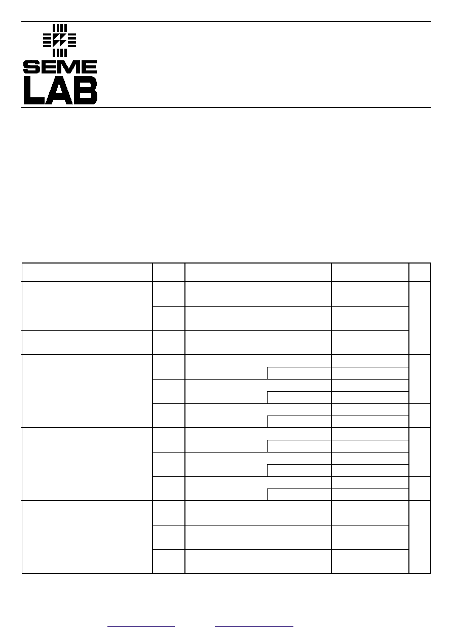
ABSOLUTE MAXIMUM RATINGS
(T
case
= 25∞C unless otherwise stated)
LOW DROPOUT
3 AMP POSITIVE
VOLTAGE REGULATOR
V
IN
Input Voltage
5V, 12V
V
I-O
Input≠Output Differential Voltage
Adjustable
P
D
Power Dissipation
V
IN
Operating Input Voltage
Adjustable
5 Volt
12 Volt
T
J
Operating Junction Temperature Range
Control
Power
T
STG
Storage Temperature Range
T
LEAD
Lead Temperature (for 10 sec.)
30V
35V
Internally limited
25V
20V
25V
≠55 to 150∞C
≠55 to 200∞C
≠65 to 150∞C
300∞C
FEATURES
∑ Low Dropout Performance
∑ Fixed or Adjustable Voltages
∑ Fixed Output Voltages of 5V & 12V
∑ Output Current 3A
∑ Line Regulation 0.015% / V Typical.
∑ Load Regulation 0.1% Typical.
∑ Military Temperature Range (≠55 to +150∞C)
IN
V
THERMAL
LIMIT
ADJ
V
OUT
V
* Although the devices' maximum operating voltage is limited (20V for the 5V device, and 25V for the 12V and adjustable devices) the devices are
guaranteed to withstand transient input voltages up to 30V. For input voltages greater than the maximum operating input voltage, some degradation of
specifications will occur. For 5V and 12V devices operating at input-output voltage differentials >15V, a minimum external load of 5mA is required to
maintain regulation.
BLOCK DIAGRAM
Prelim. 10/95
LT1085≠220M
≠05
LT1085≠05≠220M
LT1085≠12≠220M
MILITARY VERSION
Semelab plc.
Telephone +44(0)1455 556565. Fax +44(0)1455 552612.
E-mail:
sales@semelab.co.uk
Website:
http://www.semelab.co.uk
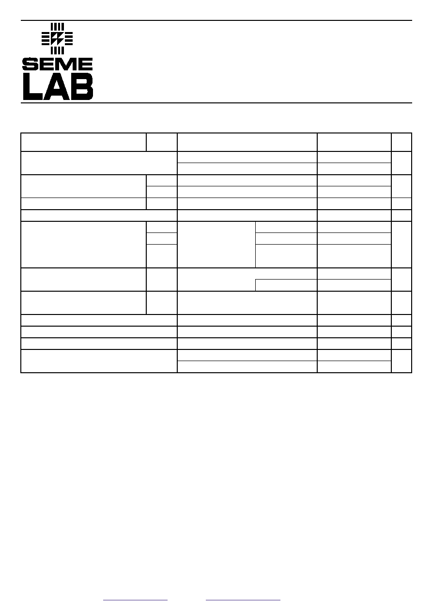
V
O
Output Voltage
V
REF
Reference Voltage
REG
(LINE)
Line Regulation
REG
(LOAD)
Load Regulation
See notes 1,2
V
D
Dropout Voltage
See note 3
Output
Parameter
Voltage Test Conditions
Min.
Typ. Max.
Unit
V
IN
= 6.5 to 20V
I
O
= 0 to 3A
T
J
= ≠55 to 150∞C
V
IN
= 13.5V to 25V
I
O
= 0 to 3A
T
J
= ≠55 to 150∞C
V
IN
≠ V
OUT
= 1.5 to 15V
I
O
= 10mA to 3A
T
J
= ≠55 to 150∞C
V
IN
= 6.5 to 20V
I
O
= 0
T
J
= ≠55 to 150∞C
V
IN
= 13.5 to 25V
I
O
= 0
T
J
= ≠55 to 150∞C
V
IN
≠ V
OUT
= 1.5 to 15V
I
LOAD
= 10mA
T
J
= ≠55 to 150∞C
V
IN
= 8V
I
O
= 0 to 3A
T
J
= ≠55 to 150∞C
V
IN
= 15V
I
O
= 0 to 3A
T
J
= ≠55 to 150∞C
V
IN
≠ V
OUT
= 3V
I
O
= 10mA to 3A
T
J
= ≠55 to 150∞C
D
V
OUT
= 50mV
I
OUT
= 3A
T
J
= ≠55 to 150∞C
D
V
OUT
= 120mV
I
OUT
= 3A
T
J
= ≠55 to 150∞C
D
V
REF
= 1%
I
OUT
= 3A
T
J
= ≠55 to 150∞C
4.90
5
5.10
11.76
12
12.24
1.225
1.25
1.270
0.5
10
1
10
1
25
2
25
0.015
0.2
0.035
0.2
5
20
10
35
12
36
24
72
0.1
0.3
0.2
0.4
1.3
1.5
1.3
1.5
1.3
1.5
5
12
ADJ.
5
12
ADJ.
5
12
ADJ.
5
12
ADJ.
ELECTRICAL CHARACTERISTICS
(T
J
= 25∞C unless otherwise stated)
V
mV
%
mV
%
V
DESCRIPTION
The LT1085 is designed to provide 3A with higher efficiency than currently available devices. All internal circuitry is
designed to operate down to 1V input to output differential and the dropout voltage is fully specified as a function of load
current. Dropout is guaranteed at a maximum of 1.5V at maximum output current, decreasing at lower load currents.
On-chip trimming adjusts the reference output voltage to 1%. Current limit is also trimmed, minimising the stress on both
the regulator and power source circuitry under overload conditions.
The LT1085 is pin compatible with older 3 terminal adjustable regulators. A 10
m
F output capacitor is required on these
new devices; however, this is usually included in most regulator designs.
Unlike PNP regulators, where up to 10% of the output current is wasted as quiescent current, the LT1085 quiescent
current flows into the load, increasing efficiency.
Prelim. 10/95
LT1085≠220M
≠05
LT1085≠05≠220M
LT1085≠12≠220M
MILITARY VERSION
Semelab plc.
Telephone +44(0)1455 556565. Fax +44(0)1455 552612.
E-mail:
sales@semelab.co.uk
Website:
http://www.semelab.co.uk
I
CL
Current Limit
I
Q
Quiescent Current
Minimum Load Current
4
REG
(THERM)
Thermal Regulation
R
A
Ripple Rejection
I
PIN
Adjust Pin Current
D
I
PIN
Adjust Pin Current Change
T
S
Temperature Stability
Long Term Stability
V
N
RMS Output Noise
R
q
JC
Thermal Resistance
Junction ≠ Case
Output
Parameter
Voltage Test Conditions
Min.
Typ. Max.
Unit
V
IN
≠ V
OUT
= 5V
T
J
= ≠55 to 150∞C
V
IN
≠ V
OUT
= 25V
T
J
= ≠55 to 150∞C
V
IN
£
20V
T
J
= ≠55 to 150∞C
V
IN
£
25V
T
J
= ≠55 to 150∞C
V
IN
≠ V
OUT
= 25V
T
J
= ≠55 to 150∞C
T
P
= 30ms
T
A
= 25∞C
T
J
= ≠55 to 150∞C
V
IN
= 8V
C
OUT
= 25
m
F Tantalum
V
IN
= 15V
f = 120Hz
V
IN
≠ V
OUT
= 3V
I
O
= 3A
C
ADJ
= 25
m
F
T
J
= ≠55 to 150∞C
V
IN
≠ V
OUT
= 1.5 to 15V
I
O
= 10mA to 3A
T
J
= ≠55 to 150∞C
T
J
= ≠55 to 150∞C
T
A
= 125∞C
T = 1000 Hrs
f = 10Hz to 10kHz
T
A
= 25∞C
Control Circuitry
Power Transistor
3.2
4
0.2
0.5
5
10
5
10
5
10
0.004
0.02
60
68
54
60
60
75
55
120
0.2
5
0.5
0.3
1
0.003
TBA
TBA
5
12
ADJ.
5
12
ADJ.
ADJ.
ADJ.
ELECTRICAL CHARACTERISTICS
(T
J
= ≠55 to +150∞C unless otherwise stated)
A
mA
%/W
dB
m
A
m
A
%
%
%
∞C/W
Notes:
1. See thermal regulation specifications for changes in output voltage due to heating effects. Load and line regulation are
measured at a constant junction temperature by low duty cycle pulse testing. Load regulation is measured at the output
lead
ª
1/
8
" from the package.
2. Line and load regulation are guaranteed up to the maximum power dissipation of 30W. Power dissipation is determined
by the input - output differential and the output current. Guaranteed maximum power dissipation will not be available over
the full input - output voltage range.
3. Dropout voltage is specified over the full output current range of the device.