Copyright
2002
Semicoa Semiconductors, Inc.
Rev. F
333 McCormick Avenue, Costa Mesa, California 92626 714.979.1900, FAX 714.557.4541
Page 1 of 2
www.SEMICOA.com
2N2484
Silicon NPN Transistor
Data Sheet
Description
Semicoa Semiconductors offers:
∑ Screening and processing per MIL-PRF-19500
Appendix E
∑ JAN level (2N2484J)
∑ JANTX level (2N2484JX)
∑ JANTXV level (2N2484JV)
∑ JANS level (2N2484JS)
∑ QCI to the applicable level
∑ 100% die visual inspection per MIL-STD-750 method
2072 for JANTXV and JANS
∑ Radiation testing (total dose) upon request
Please contact Semicoa for special configurations
www.SEMICOA.com or (714) 979-1900
Applications
∑ General purpose
∑ Low power
∑ NPN silicon transistor
Features
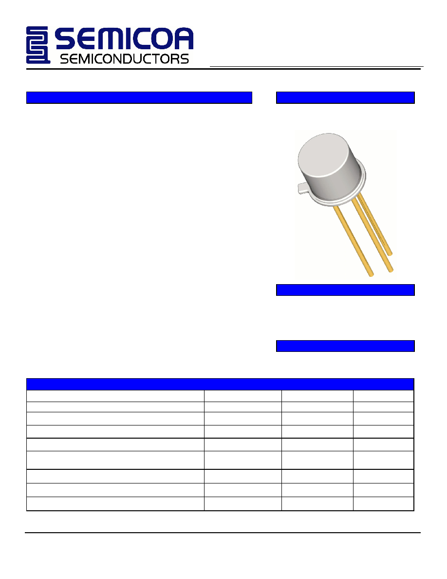
∑ Hermetically sealed TO-18 metal can
∑ Also available in chip configuration
∑ Chip geometry 0307
∑ Reference document:
MIL-PRF-19500/376
Benefits
∑ Qualification Levels: JAN, JANTX,
JANTXV and JANS
∑ Radiation testing available
Absolute Maximum Ratings
T
C
= 25
∞C unless otherwise specified
Parameter Symbol
Rating
Unit
Collector-Emitter Voltage
V
CEO
60
Volts
Collector-Base Voltage
V
CBO
60
Volts
Emitter-Base Voltage
V
EBO
6
Volts
Collector Current, Continuous
I
C
50
mA
Power Dissipation, T
A
= 25
∞C
Derate linearly above 25
∞C
P
T
360
2.06
mW
mW/
∞C
Thermal Resistance
R
JA
325
∞C/W
Operating Junction Temperature
T
J
-65 to +200
∞C
Storage Temperature
T
STG
-65 to +200
∞C
Copyright
2002
Semicoa Semiconductors, Inc.
Rev. F
333 McCormick Avenue, Costa Mesa, California 92626 714.979.1900, FAX 714.557.4541
Page 2 of 2
www.SEMICOA.com
2N2484
Silicon NPN Transistor
Data Sheet
ELECTRICAL CHARACTERISTICS
characteristics specified at T
A
= 25
∞C
Off Characteristics
Parameter Symbol
Test
Conditions
Min
Typ
Max
Units
Collector-Emitter Breakdown Voltage
V
(BR)CEO
I
C
= 10 mA
60
Volts
Collector-Base Cutoff Current
I
CBO1
I
CBO2
I
CBO3
V
CB
= 60 Volts
V
CB
= 45 Volts
V
CB
= 45 Volts, T
A
= 150
∞C
10
5
10
µA
nA
µA
Collector-Emitter Cutoff Current
I
CEO
V
CE
= 5 Volts
2
nA
Collector-Emitter Cutoff Current
I
CES
V
CE
= 45 Volts
5
nA
Emitter-Base Cutoff Current
I
EBO1
I
EBO2
V
EB
= 6 Volts
V
EB
= 5 Volts
10
2
µA
nA
On Characteristics
Pulse Test: Pulse Width = 300
µs, Duty Cycle 2.0%
Parameter Symbol
Test
Conditions
Min
Typ
Max
Units
DC Current Gain
h
FE1
h
FE2
h
FE3
h
FE4
h
FE5
h
FE6
h
FE7
I
C
= 1
µA, V
CE
= 5 Volts
I
C
= 10
µA, V
CE
= 5 Volts
I
C
= 100
µA, V
CE
= 5 Volts
I
C
= 500
µA, V
CE
= 5 Volts
I
C
= 1 mA, V
CE
= 5 Volts
I
C
= 10 mA, V
CE
= 5 Volts
I
C
= 10
µA, V
CE
= 5 Volts
T
A
= -55
∞C
45
200
225
250
250
225
35
500
675
800
800
800
Base-Emitter Voltage
V
BE
V
CE
= 5 Volts, 100
µA
0.5 0.7
Volts
Collector-Emitter Saturation Voltage
V
CEsat1
I
C
= 1 mA, I
B
= 100
µA
0.3
Volts
Dynamic Characteristics
Parameter Symbol
Test
Conditions
Min
Typ
Max
Units
Magnitude ≠ Common Emitter, Short
Circuit Forward Current Transfer Ratio
|h
FE
|
1
|h
FE
|
2
V
CE
= 5 Volts, I
C
= 50
µA,
f = 5 MHz
V
CE
= 5 Volts, I
C
= 500
µA,
f = 30 MHz
3
2
7
Small Signal Short Circuit Forward
Current Transfer Ratio
h
FE
V
CE
= 5 Volts, I
C
= 1 mA,
f = 1 kHz
250 900
Open Circuit Output Capacitance
C
OBO
V
CB
= 5 Volts, I
E
= 0 mA,
100 kHZ < f < 1 MHz
5
pF
Open Circuit Input Capacitance
C
IBO
V
EB
= 0.5 Volts, I
C
= 0 mA,
100 kHZ < f < 1 MHz
6
pF
Noise Figure
NF
1
NF
2
NF
3
V
CE
= 5 Volts, I
C
= 10
µA,
R
g
= 10 k
f = 100 Hz
f = 1 kHz
f = 10 kHz
7.5
3
2
dB
Noise Figure (wideband)
NF
4
V
CE
= 5 Volts, I
C
= 10
µA,
R
g
= 10 k
,
10Hz < Noise BW <15.7kHz
3
dB
Short Circuit Input Impedance
Open Circuit Output Admittance
Open Circuit Rev Volt Transfer Ratio
h
ie
h
oe
h
re
V
CB
= 5V, I
C
= 1mA, f = 1kHz
3.5
24
40
8x10
-4
k
µmhos