
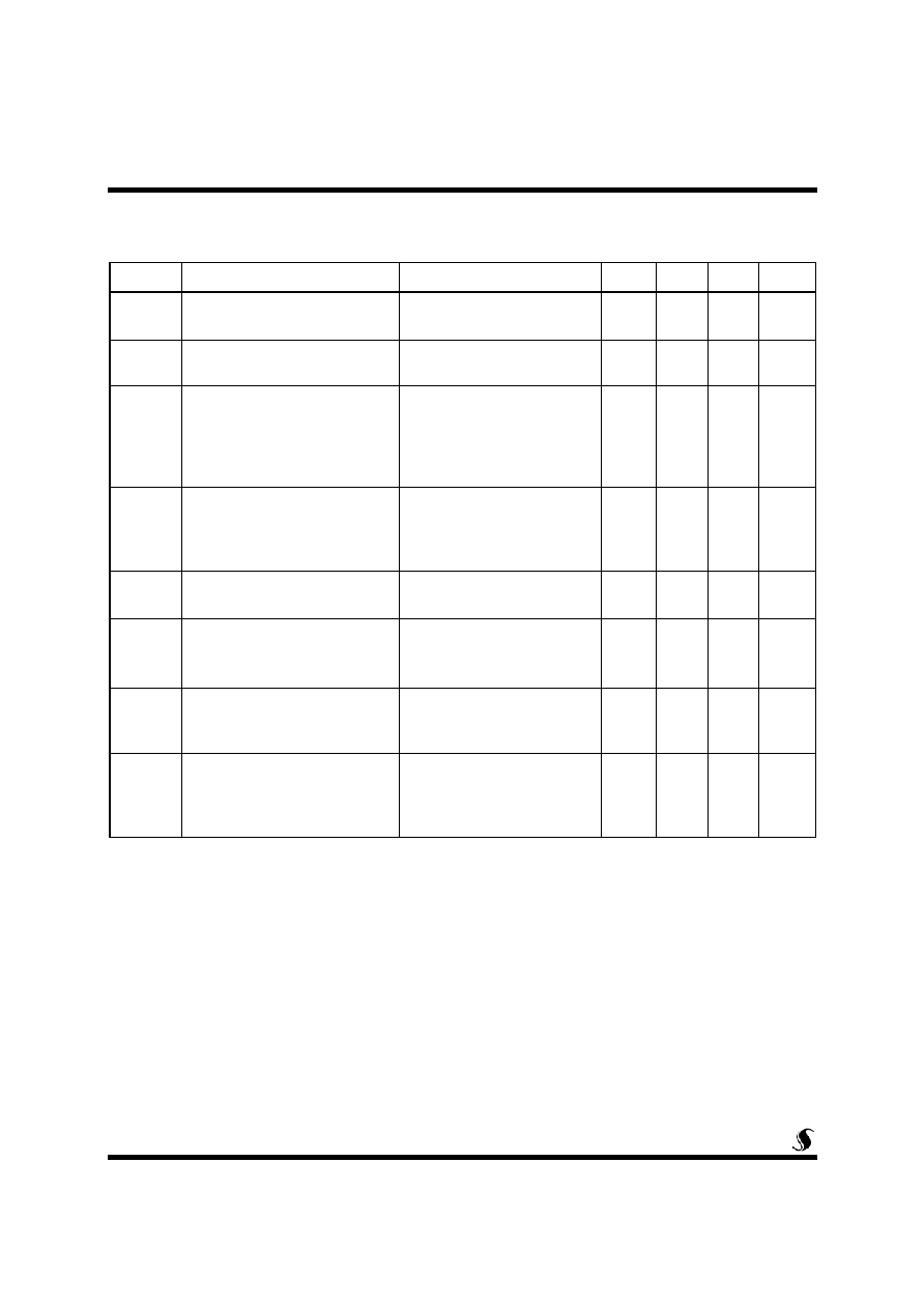
Absolute Maximum Ratings
Symbol
Parameter
Value
Units
V
CES
Collector-Emitter Voltage ( V
BE
= 0 )
700
V
V
CEO
Collector-Emitter Voltage ( I
B
= 0 )
400
V
V
EBO
Emitter-Base Voltage ( I
C
= 0 )
9.0
V
I
C
Collector Current
12
A
I
CM
Collector Peak Current ( t
P
10 ms )
25
A
I
B
Base Current
6.0
A
I
BM
Base Peak Current ( t
P
10 ms )
12
A
P
C
Total Dissipation at T
C
= 25 �C
100
W
T
STG
Storage Temperature
- 65 ~ 150
�C
T
J
Max. Operating Junction Temperature
150
�C
Thermal Characteristics
Symbol
Parameter
Value
Units
R
JC
Thermal Resistance, Junction-to-Case
1.25
�C/W
R
JA
Thermal Resistance, Junction-to-Ambient
40
�C/W
SBP13009A
May, 2003. Rev. 3
1/6
Features
- Very High Switching Speed (Typical 60ns@8.0A)
- Minimum Lot-to-Lot hFE Variation
- Low VCE(sat) (Typical 320mV@8.0A/1.6A)
- Wide Reverse Bias S.O.A
General Description
This device is designed for high voltage, high speed switching char-
acteristic required such as lighting system, switching mode power
supply.
High Voltage Fast-Switching NPN Power Transistor
2.Collector
3.Emitter
1.Base
Symbol
TO-220
SemiWell
Semiconductor
1
2
3
Copyright@SemiWell Semiconductor Co., Ltd., All rights reserved
Electrical Characteristics
( T
C
= 25 �C unless otherwise noted )
Symbol
Parameter
Condition
Min
Typ
Max
Units
I
CEV
Collector Cut-off Current
( V
BE
= - 1.5V )
V
CE
= 700V
V
CE
= 700V T
C
= 100 �C
-
-
1.0
5.0
mA
V
CEO(sus)
Collector-Emitter Sustaining Voltage
( I
B
= 0 )
I
C
= 10 mA
400
-
-
V
V
CE(sat)
Collector-Emitter Saturation Voltage
I
C
= 5.0A I
B
= 1.0A
I
C
= 8.0A I
B
= 1.6A
I
C
= 12A I
B
= 3.0A
I
C
= 8.0A I
B
= 1.6A
T
C
= 100 �C
-
-
0.5
1.0
1.5
2.0
V
V
BE(sat)
Base-Emitter Saturation Voltage
I
C
= 5.0A I
B
= 1.0A
I
C
= 8.0A I
B
= 1.6A
I
C
= 8.0A I
B
= 1.6A
T
C
= 100 �C
-
-
1.2
1.6
1.5
V
h
FE
DC Current Gain
I
C
= 5.0A V
CE
= 5V
I
C
= 8.0A V
CE
= 5V
10
6
-
40
40
t
s
t
f
Resistive Load
Storage Time
Fall Time
I
C
= 8.0A V
CC
= 125V
I
B1
= 1.6A I
B2
= - 1.6A
T
P
= 25
-
3.0
0.4
t
s
t
f
Inductive Load
Storage Time
Fall Time
V
CC
= 15V I
C
= 8.0A
I
B1
= 1.6A V
BE(off)
= 5V
L
C
= 0.2mH V
clamp
= 300V
-
2.0
0.3
t
s
t
f
Inductive Load
Storage Time
Fall Time
V
CC
= 15V I
C
= 8.0A
I
B1
= 1.6A V
BE(off)
= 5V
L
C
= 0.2mH V
clamp
= 300V
T
C
= 100 �C
-
2.5
0.4
SBP13009A
2/6
Notes :
Pulse Test : Pulse width 300, Duty cycle 2%

0
1
2
3
4
5
6
7
8
9
10
11
12
13
1
10
T
J
= 25
o
C
t,
T
i
m
e
[us]
I
C
, Collector Current [A]
0
2
4
6
8
10
12
14
10
100
1000
T
J
= 25
o
C
t, Ti
me
[n
s]
I
C
, Collector Current [A]
0
1
2
3
4
5
6
7
8
9
10
0
2
4
6
8
10
12
14
16
18
I
B
= 1400mA
I
B
= 1800mA
I
B
= 0mA
I
B
= 200mA
I
B
= 400mA
I
B
= 600mA
I
B
= 800mA
I
B
= 1000mA
I
B
= 1200mA
I
B
= 1600mA
I
B
= 2000mA
I
C
, C
o
lle
c
to
r
Cu
r
r
e
n
t
[A]
V
CE
, Collector-Emitter Voltage [V]
0.1
1
10
0.2
0.4
0.6
0.8
1.0
1.2
1.4
T
J
= 25
o
C
T
J
= 125
o
C
V
BE
, Ba
se
-
E
mi
tt
e
r
Vo
l
t
a
g
e
[V]
I
C
, Collector Current [A]
0.1
1
10
0.01
0.1
1
10
T
J
= 25
o
C
T
J
= 125
o
C
V
CE
,
Collect
o
r
-
E
mit
t
er Volt
ag
e [
V
]
I
C
, Collector Current [A]
0.01
0.1
1
10
0
5
10
15
20
25
30
35
40
45
50
55
60
T
J
= 125
o
C
T
J
= 25
o
C
h
FE
, DC C
u
rrent Gain
I
C
, Collector Current [A]
SBP13009A
3/6
Fig 1. Static Characteristics
Fig 2. DC Current Gain
Fig 3. Collector-Emitter Saturation Voltage
Fig 4. Base-Emitter Saturation Voltage
Fig 5. Resistive Load Fall Time
Fig 6. Resistive Load Storage Time
Note :
h
FE
= 5
Note :
h
FE
= 5
Notes :
V
CC
= 125V
h
FE
= 5
I
B1
= - I
B2
Notes :
V
CC
= 125V
h
FE
= 5
I
B1
= - I
B2
Notes :
V
CE
= 5V
V
CE
= 1V

10
0
10
1
10
2
10
3
10
-2
10
-1
10
0
10
1
10
2
100
�
s
10
�
s
1ms
DC
I
C
, C
o
l
l
ecto
r
C
u
r
re
nt
[
A
]
V
CE
, Collector-Emitter Clamp Voltage [V]
0
50
100
150
200
0
25
50
75
100
125
P
o
we
r
De
r
a
t
i
n
g
F
a
c
t
o
r
(
%
)
T
C
, Case Temperature (
o
C)
0
100
200
300
400
500
600
700
800
0
3
6
9
12
15
-3V
-1.5V
-5V
V
BE
(off)
I
C
, C
o
l
l
ecto
r
C
u
rr
e
n
t
[A]
V
CE
, Collector-Emitter Clamp Voltage [V]
4/6
SBP13009A
Fig 8. Reverse Biased Safe Operation
Areas
Fig 7. Safe Operation Areas
Fig 9. Power Derating Curve
Single Pulse
Notes :
T
C
100 �C
Gain 4
L
C
= 0.5 mH

I
B1
V
BE
(off)
R
BB
I
B
I
C
V
Clamp
V
CC
V
CE
D.U.T
L
C
I
B1
V
BE
(off)
R
BB
I
B
I
C
V
CC
V
CE
D.U.T
R
C
SBP13009A
5/6
Inductive Load Switching & RBSOA Test Circuit
Resistive Load Switching Test Circuit