
PROTECTION PRODUCTS
1
www.semtech.com
PROTECTION PRODUCTS - MicroClamp
TM
uClamp3304A
µClamp
TM
4-Line ESD protection Array
Description
Features
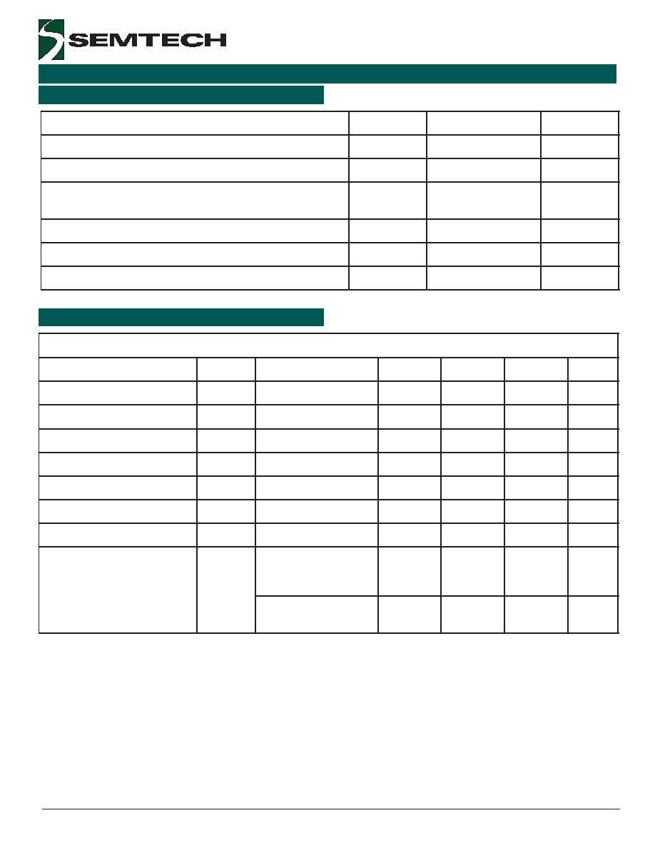
Dimensions
Schematic & PIN Configuration
Revision 02/25/05
The
µ
Clamp
TM
series of TVS arrays are designed to pro-
tect sensitive electronics from damage or latch-up due
to ESD. They are designed for use in applications where
board space is at a premium. Each device requires less
than 2.9mm
2
of PCB area and will protect up to four
lines. They are unidirectional devices and may be used
on lines with positive signal polarities.
The
µ
clamp
TM
3304A is constructed using Semtech's pro-
prietary EPD process technology. The EPD process pro-
vides low standoff voltages with significant reductions in
leakage currents and capacitance over silicon-avalanche
diode processes. They feature a true operating voltage
of 3.3 volts for superior protection when compared to
traditional pn junction devices.
These devices may be used to meet the immunity re-
quirements of IEC 61000-4-2, level 4. They offer desir-
able characteristics for board level protection including
fast response time, low operating and clamping voltage,
and no device degradation. The small SC89 package
makes them ideal for use in portable electronics such as
cell phones, PDAs, notebook computers, and digital cam-
eras.
Applications
Mechanical Characteristics
Cellular Handsets and Accessories
Cordless Phones
Notebooks and Handhelds
Portable Instrumentation
Digital Cameras
Peripherals
MP3 Players
Transient protection for data lines to
IEC 61000-4-2 (ESD) ±15kV (air), ±8kV (contact)
IEC 61000-4-4 (EFT) 40A (5/50ns)
Protects four unidirectional I/O lines
Ultra-small SC-89 package (1.7 x 1.7 x 0.6mm
1.7 x 1.7 x 0.6mm
1.7 x 1.7 x 0.6mm
1.7 x 1.7 x 0.6mm
1.7 x 1.7 x 0.6mm)
requires less than 2.9mm
2
of PCB area
Working voltage: 3.3V
Low leakage current
Low operating and clamping voltages
Solid-state silicon-avalanche technology
SC-89 (SOT-666) package
Molding compound flammability rating: UL 94V-0
Marking: Marking Code
Lead Finish: Matte Tin
RoHS Compliant
Weight: 2.9mg (typical)
Packaging: Tape and Reel per EIA 481
SC-89 (Top View)
0.60
1.70
1.70
1.25
0.30
0.50
Maximum Dimensions (mm)
2
2005 Semtech Corp.
www.semtech.com
PROTECTION PRODUCTS
µClamp3304A
Absolute Maximum Rating
Electrical Characteristics (T=25
o
C)
r
e
t
e
m
a
r
a
P
l
o
b
m
y
S
s
n
o
i
t
i
d
n
o
C
m
u
m
i
n
i
M
l
a
c
i
p
y
T
m
u
m
i
x
a
M
s
t
i
n
U
e
g
a
tl
o
V
f
f
O
-
d
n
a
t
S
e
s
r
e
v
e
R
V
M
W
R
3
.
3
V
e
g
a
tl
o
V
h
g
u
o
r
h
T
-
h
c
n
u
P
V
T
P
I
T
P
A
µ
2
=
5
.
3
V
e
g
a
tl
o
V
k
c
a
B
-
p
a
n
S
V
B
S
I
B
S
A
m
0
5
=
8
.
2
V
t
n
e
r
r
u
C
e
g
a
k
a
e
L
e
s
r
e
v
e
R
I
R
V
M
W
R
V
3
.
3
=
5
0
.
0
5
.
0
A
µ
e
g
a
tl
o
V
g
n
i
p
m
a
l
C
V
C
I
P
P
s
µ
0
2
/
8
=
p
t
,
A
1
=
5
.
5
V
e
g
a
tl
o
V
g
n
i
p
m
a
l
C
V
C
I
P
P
s
µ
0
2
/
8
=
p
t
,
A
5
=
0
.
8
V
e
g
a
tl
o
V
g
n
i
p
m
a
l
C
e
s
r
e
v
e
R
V
R
C
I
P
P
s
µ
0
2
/
8
=
p
t
,
A
1
=
4
.
2
V
e
c
n
a
ti
c
a
p
a
C
n
o
it
c
n
u
J
C
j
d
n
G
o
t
n
i
p
O
/
I
V
R
z
H
M
1
=
f
,
V
0
=
2
2
0
3
F
p
d
n
G
o
t
n
i
p
O
/
I
V
R
z
H
M
1
=
f
,
V
3
.
3
=
4
1
F
p
g
n
i
t
a
R
l
o
b
m
y
S
e
u
l
a
V
s
t
i
n
U
)
s
µ
0
2
/
8
=
p
t
(
r
e
w
o
P
e
s
l
u
P
k
a
e
P
P
k
p
0
4
s
t
t
a
W
(
t
n
e
r
r
u
C
e
s
l
u
P
k
a
e
P
m
u
m
i
x
a
M
)
s
µ
0
2
/
8
=
p
t
I
p
p
5
s
p
m
A
)
r
i
A
(
2
-
4
-
0
0
0
1
6
C
E
I
r
e
p
D
S
E
)
t
c
a
t
n
o
C
(
2
-
4
-
0
0
0
1
6
C
E
I
r
e
p
D
S
E
V
P
P
0
2
-
/
+
5
1
-
/
+
V
k
e
r
u
t
a
r
e
p
m
e
T
g
n
ir
e
d
l
o
S
d
a
e
L
T
L
).
c
e
s
0
1
(
0
6
2
C
∞
e
r
u
t
a
r
e
p
m
e
T
g
n
it
a
r
e
p
O
T
J
5
2
1
+
o
t
5
5
-
C
∞
e
r
u
t
a
r
e
p
m
e
T
e
g
a
r
o
t
S
T
G
T
S
0
5
1
+
o
t
5
5
-
C
∞

3
2005 Semtech Corp.
www.semtech.com
PROTECTION PRODUCTS
µClamp3304A
Typical Characteristics
Non-Repetitive Peak Pulse Power vs. Pulse Time
0
10
20
30
40
50
60
70
80
90
100
110
0
25
50
75
100
125
150
Ambient Temperature - T
A
(
o
C)
%
of
Rat
e
d Power
or
I
PP
Power Derating Curve
Clamping Voltage vs. Peak Pulse Current
Junction Capacitance vs. Reverse Voltage
Forward Voltage vs Forward Current
ESD Clamping
(8kV Contact per IEC 61000-4-2)
0.0
5.0
10.0
15.0
20.0
25.0
0
0.5
1
1.5
2
2.5
3
3.5
Reverse Voltage - V
R
(V)
Capa
ci
t
a
nc
e -
C
j
(
pF)
f = 1 MHz
0
2
4
6
8
10
12
0
1
2
3
4
5
Peak Pulse Current - I
PP
(A)
Cl
a
m
pi
ng Vol
t
a
g
e -
V
C
(V
)
Waveform
Parameters:
tr = 8µs
td = 20µs
0.01
0.1
1
0.1
1
10
100
1000
Pulse Duration - tp (µs)
Pea
k
Pul
se Power
-
P
PP
(k
W
)
0
1
2
3
4
5
6
7
0
1
2
3
4
5
6
Forward Current - I
F
(A)
Forwa
rd Vo
l
t
a
g
e
-
V
F
(V
)
Waveform
Parameters:
tr = 8µs
td = 20µs

4
2005 Semtech Corp.
www.semtech.com
PROTECTION PRODUCTS
µClamp3304A
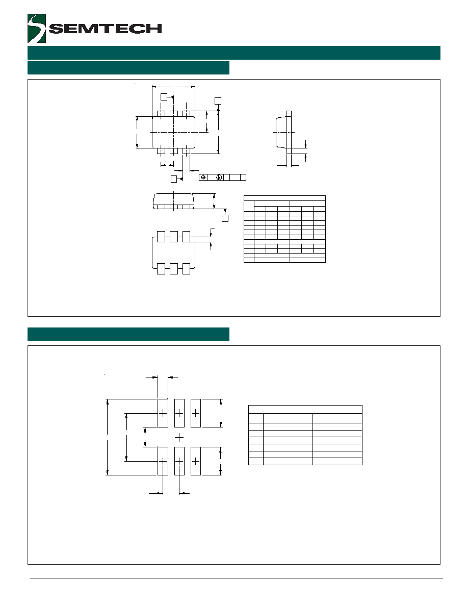
Circuit Diagram
Protection of Four Unidirectional Lines
Device Connection for Protection of Four Data Lines
These devices are designed to protect up to four
unidirectional data lines. The device is connected as
follows:
1. Unidirectional protection of four I/O lines is
achieved by connecting pins 1, 3, 4, and 6 to the
data lines. Pins 2 and 5 are connected to ground.
The ground connection should be made directly to
the ground plane for best results. The path length
is kept as short as possible to reduce the effects
of parasitic inductance in the board traces.
Circuit Board Layout Recommendations for Suppres-
sion of ESD.
Good circuit board layout is critical for the suppression
of ESD induced transients. The following guidelines are
recommended:
Place the TVS near the input terminals or connec-
tors to restrict transient coupling.
Minimize the path length between the TVS and the
protected line.
Minimize all conductive loops including power and
ground loops.
The ESD transient return path to ground should be
kept as short as possible.
Never run critical signals near board edges.
Use ground planes whenever possible.
Matte Tin Lead Finish
Matte tin has become the industry standard lead-free
replacement for SnPb lead finishes. A matte tin finish
is composed of 100% tin solder with large grains.
Since the solder volume on the leads is small com-
pared to the solder paste volume that is placed on the
land pattern of the PCB, the reflow profile will be
determined by the requirements of the solder paste.
Therefore, these devices are compatible with both
lead-free and SnPb assembly techniques. In addition,
unlike other lead-free compositions, matte tin does not
have any added alloys that can cause degradation of
the solder joint.
Applications Information
2, 5
1
3
4
6

5
2005 Semtech Corp.
www.semtech.com
PROTECTION PRODUCTS
µClamp3304A
Typical Applications
uClamp3304A

6
2005 Semtech Corp.
www.semtech.com
PROTECTION PRODUCTS
µClamp3304A
Applications Information - Spice Model
Figure 1 - µClamp3304A Spice Model
s
r
e
t
e
m
a
r
a
P
e
c
i
p
S
A
4
0
3
3
p
m
a
l
C
µ
-
1
e
l
b
a
T
r
e
t
e
m
a
r
a
P
t
i
n
U
)
S
V
T
(
1
D
)
D
R
C
L
(
2
D
S
I
p
m
A
0
2
-
E
0
0
.
1
0
2
-
E
0
0
.
1
V
B
tl
o
V
7
4
.
3
8
J
V
tl
o
V
4
1
0
7
.
0
S
R
m
h
O
7
3
7
.
0
5
9
7
.
0
V
B
I
p
m
A
3
-
E
0
.
1
3
-
E
0
.
1
O
J
C
d
a
r
a
F
2
1
-
E
3
5
.
4
1
2
1
-
E
6
T
T
c
e
s
9
-
E
1
4
5
.
2
9
-
E
1
4
5
.
2
M
--
2
5
1
.
0
2
5
1
.
0
N
--
1
.
1
1
.
1
G
E
V
e
1
1
.
1
1
1
.
1
7
2005 Semtech Corp.
www.semtech.com
PROTECTION PRODUCTS
µClamp3304A
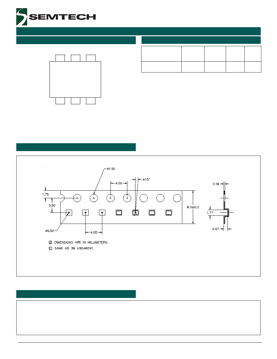
Outline Drawing - SC-89 (SOT-666)
Land Pattern - SC-89 (SOT-666)
INCHES
.063
N
c
E1
E
L
D
.059
.043
DIM
A
MIN
.019
1.70
1.25
1.50
1.10
6
-
.008
.063
.047
.067
.049
6
-
0.20
1.60
1.20
1.60
MILLIMETERS
MAX
0.60
MIN
DIMENSIONS
MAX
NOM
-
.024
NOM
0.50
-
1
A
B
C
CONTROLLING DIMENSIONS ARE IN MILLIMETERS (ANGLES IN DEGREES).
NOTES:
OR GATE BURRS.
DIMENSIONS "E1" AND "D" DO NOT INCLUDE MOLD FLASH, PROTRUSIONS
2.
1.
1.70
1.55
.061
.067
0.30
0.10
.012
.003
L1
.003 .006
0.15
0.10
.008
0.20
b
.005
-
-
0.15
.012
0.30
e
.020 BSC
0.50 BSC
0.18
0.10
.007
.003
aaa
C A-B D
D
e
Nxb
2
E/2
D
E1
E
c
L
N
A
L1
aaa
.004
0.10
NOTES:
1. THIS LAND PATTERN IS FOR REFERENCE PURPOSES ONLY
CONSULT YOUR MANUFACTURING GROUP TO ENSURE YOUR
COMPANY'S MANUFACTURING GUIDELINES ARE MET.
DIM
Y
Z
G
X
C
MILLIMETERS
INCHES
(1.45)
.033
.090
.012
.024
(.057)
0.85
2.30
0.30
0.60
DIMENSIONS
Z
X
Y
C
G
Y
P
0.50
.020
P
8
2005 Semtech Corp.
www.semtech.com
PROTECTION PRODUCTS
µClamp3304A
Contact Information
Semtech Corporation
Protection Products Division
200 Flynn Rd., Camarillo, CA 93012
Phone: (805)498-2111 FAX (805)498-3804
Marking Code
Ordering Information
Note:
(1) Device is symmetrical so there is no pin 1 identifier
Tape and Reel Specification
Tape Specifications and Device Orientation
Note: Lead finish is lead-free matte tin
MicroClamp, uClamp and µClamp are trademarks of Semtech
Corporation
r
e
b
m
u
N
t
r
a
P
g
n
i
k
r
o
W
e
g
a
t
l
o
V
e
c
i
v
e
D
g
n
i
k
r
a
M
r
e
p
y
t
Q
l
e
e
R
l
e
e
R
e
z
i
S
T
C
T
.
A
4
0
3
3
p
m
a
l
C
u
V
3
.
3
S
S
0
0
0
,
3
h
c
n
I
7
SS
SS
SS
SS