 | –≠–ª–µ–∫—Ç—Ä–æ–Ω–Ω—ã–π –∫–æ–º–ø–æ–Ω–µ–Ω—Ç: XE1201A | –°–∫–∞—á–∞—Ç—å:  PDF PDF  ZIP ZIP |
90 DEG
90 DEG
FILTERING +
OFFSET
REDUCTION
DEMODULATOR
SYMBOL SYNCHRO
RF POWER AMP
EN
DDS
LO
RXTX
RXD
CLOCK
DVDD
DGND
SD
BUS CONTROL
POWER MANAGEMENT
CLKD
DE
SC
TXD
AVDD
AGND
RFGND
RFVDD
TLA
SWB
SWA
TKA
TKB
TKC
XTAL
TLB
RFA
RFB
RFOUT
IO
QO
VREF
TPA
TPB
LOGND
Data Sheet XE1201A
Low Power UHF Transceiver
XE1201A 300-500 MHz
XE1201A 300-500 MHz
Low-Power UHF Transceiver
Low-Power UHF Transceiver
Features
Features
∑
very
low-power
∑
very
low-power
∑
half-duplex
operation
∑
half-duplex
operation
∑
data rate up to 64 kbit/s
∑
data rate up to 64 kbit/s
∑
high
sensitivity
∑
high
sensitivity
∑
few external components
∑
few external components
∑
internal bit synchronizer
∑
internal bit synchronizer
∑
3-wire bus for easy microcontroller
interface
∑
3-wire bus for easy microcontroller
interface
∑
output power programmable via bus
∑
output power programmable via bus
Applications
Applications
∑
telemetry
∑
telemetry
∑
RF security systems
∑
RF security systems
∑
wireless data link
∑
wireless data link
∑
door
openers
∑
door
openers
∑
remote
control
∑
remote
control
∑
wireless
sensing
∑
wireless
sensing
Ordering Information
Ordering Information
Part
Part Temperature
range
Temperature
range
Pin-package
Pin-package
XE1201A
-40 to 70
∞
C
TQFP32
General Description
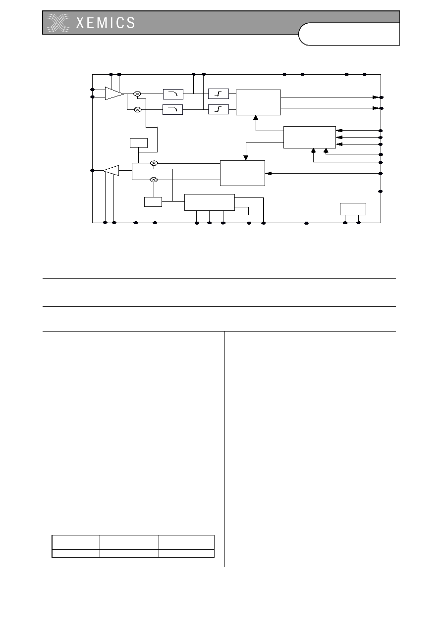
The XE1201A is a half-duplex FSK transceiver for
operation in the 433 MHz ISM band (optimized)
and in the 300-500 MHz band. The modulation
used is the Continuous Phase, 2 level Frequency
Shift Keying (CPFSK). The direct conversion (zero
IF) receiver architecture enables on-chip channel
filtering.
The XE1201A includes a bit synchronizer so that
glitch free data with synchronized clock can
directly be read by a low cost / low complexity
micro-controller. The transmitted power level can
also be controlled via the bus. The XE1201A
meets the I-ETS300-220 standard and is available
in a TQFP32 package.
Quick Reference Data
∑
supply voltage
2.4 V
∑
RF sensitivity
-109 dBm
∑
data rate
64 kbits/s
∑
transmitted power
+5 dBm
Cool Solutions for Wireless Connectivity
XEMICS SA
∑
e-mail: info@xemics.com
∑
web: www.xemics.com
Data Sheet XE1201A
Low Power UHF Transceiver
Detailed Pin Description
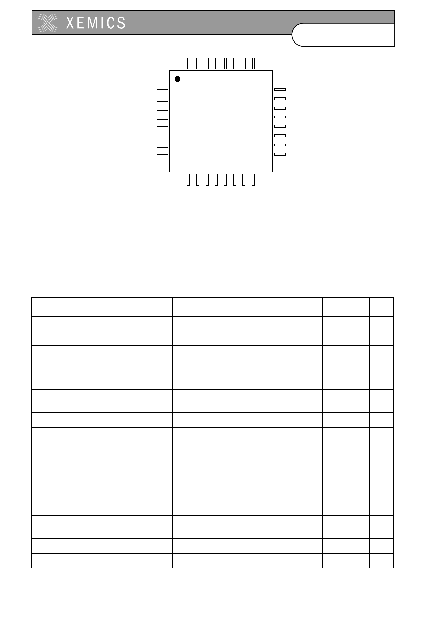
PIN NAME
DESCRIPTION
1
EN
Chip enable
2
DE
Bus data enable
3
AVDD
Supply voltage for analog
4
TPA
Power amplifier tank circuit
5
TPB
Power amplifier tank circuit
6
AGND
Ground for analog
7 SC Bus
clock
8
SD
Bus data input
9
LOGND
Ground for local oscillator
10
TKA
Oscillator tank circuit
11
TKB
Oscillator tank circuit
12
TKC
Oscillator tank circuit
13 SWA SAW
resonator
14 SWB SAW
resonator
15
RXTX
Receiver / transmitter enable
16
VREF
Voltage stabilizer decoupling
17
TXD
Data input stream
18
CLKD
Received data clock
19
RXD
Received data output
20
DGND
Ground for digital
21 XTAL
Reference
oscillator
22 XTAL
Reference
oscillator
23
DVDD
Supply voltage for digital
24 QO Test
pin
25 IO Test
pin
26
RFA
RF input
27
RFB
RF input
28
RFGND
Ground for RF
29 RFOUT
Transmitter
output
30
TLA
Low noise amplifier tank circuit
31
TLB
Low noise amplifier tank circuit
32
RFVDD
Supply voltage for RF
2
D0205-118
Data Sheet XE1201A
Low Power UHF Transceiver
fig. 2: TQFP 32L package
EN
DE
AVDD
TPA
TPB
AGND
SC
SD
LO
GN
D
TK
A
TK
B
TK
C
SW
A
SW
B
RX
TX
VR
E
F
QO
DVDD
XTAL
XTAL
DGND
RXD
CLKD
TXD
RFV
D
D
TL
B
TLA
RF
O
U
T
RFG
N
D
RFB
RFA
IO
Absolute Ratings
∑
supply voltage
2.4 V to 6 V
∑
storage temperature -55∞C to 150∞C
∑
operating temperature -40∞C to 70∞C
Electrical Characteristics
Tamb = 25∞ C; VDD = 3.0 V; F
LO
= 433.92 MHz; +/- 125 kHz frequency deviation; 16 kbit/s pseudo random bit sequence
unless otherwise specified
SYMBOL PARAMETER
CONDITIONS
Min Typ Max Units
VDD
Operating supply voltage
2.4
3.0
5.5
V
IDDR
Reception supply current
4.5
6
7.5
mA
IDDT
Transmission supply current
- 15 dBm output power
- 5 dBm output power
+ 2.5 dBm output power
+ 5 dBm output power
5.5
8
11
13.5
mA
mA
mA
mA
IDDS
Standby current
Clock running
Clock stopped
-
-
55
0.2
65
1
µ
A
µ
A
FR Frequency
range
300 - 500
MHz
TP
Transmitter output power
C13 = 0 ; C12 = 0
C13 = 0 ; C12 = 1
C13 = 1 ; C12 = 0
C13 = 1 ; C12 = 1
-15
-5
+2
+5
dBm
dBm
dBm
dBm
RFS RF
sensitivity
BER=1%, R
source
= 50
8 kbit/s
16 kbit/s
64 kbit/s
-106
-104
-99
-109
-107
-102
-
-
-
dBm
dBm
dBm
ZIN
RF input impedance
Parallel real part
Parallel capacitive part
-
-
1
4
-
-
k
pF
ZOUT RF output impedance
Parallel capacitive part
-
2.4
-
pF
CCR Co-channel
rejection
F
unw
=F
LO
±125 kHz
-12
-7
-
dB
3
D0205-118
Data Sheet XE1201A
Low Power UHF Transceiver
SYMBOL PARAMETER
CONDITIONS
Min Typ Max Units
RF
level
= RFS+3dB
BI Blocking
immunity
F
unw
=F
RF
±1MHz
RF
level
= RFS+3dB
39 43 - dB
ML
Maximum receiver input level 1 channel, BER=1%
0
-
-
dBm
BW
Baseband filter bandwidth
3 dB cutoff frequency
250
330
410
kHz
LOD
Local oscillator drift
-40 < Tamb < +70
∞ C
-
-4
-
ppm/
∞
C
LOS
Local oscillator shift
2.4 V < Vdd < 3.6 V
-
+/-8 +/-15 KHz
TBW
DDS anti-alias filter bandwidth
-
160
-
kHz
FDEV Frequency deviation
programmable by 3-wire bus
+/-4
-
+/-200 kHz
DR
Data rate
programmable by 3-wire bus
4
-
64
kbit/s
LOL
Digital input/output low level
0
-
0.4
V
HIL
Digital input/output high level
2.6
-
3
V
Tclk
Clock wake-up time
from cold start (see fig. 5)
-
2
3.5
ms
Rwu
Receiver wake-up time
from oscillator running (see fig. 4)
bit synchronizer bypassed
- 60 75
µ
s
Twu
Transmitter wake-up time
from oscillator running (see fig. 4)
-
60
75
µ
s
Tsu
Data set-up time
(see fig. 3)
125
-
-
ns
Trt
Receive to transmit switching
time
(see fig. 4)
- 15 25
µ
s
Ttr
Transmit to receive switching
time
(see fig. 4)
bit synchronizer bypassed
- 60 75
µ
s
Tr
SC bus clock rise time
-
-
50
ns
Tf
SC bus clock fall time
-
-
50
ns
FSC
SC bus clock frequency
-
-
4
MHz
Handling
All pins withstand the ESD test in accordance with the MIL-STD-883F method 3015.6 (all pins
towards substrate), human body model (2000V). The RF output (pin 29) is only protected against
negative voltage (no protection device towards VDD).
Functional Description
The XE1201A is controlled via the 3-wire serial bus by a microcontroller that addresses the 3 wires
(SD - Serial Data, SC - Serial Clock, DE - Data enable) according to the format shown in Figure 3 a
bit stream of 16 bits is fed into the internal register (SD - pin8) with the Most Significant Bit (MSB)
first and is shifted during the low to high transition of the clock (SC - pin7). This serial programming
is enabled by the Data Enable pin (DE - pin2) which must be set to zero before the data transfer.
The low to high transition of the Data Enable validates the register filling. Data is retained as long
as the supply voltage (Vdd) is present.
4
D0205-118
Data Sheet XE1201A
Low Power UHF Transceiver
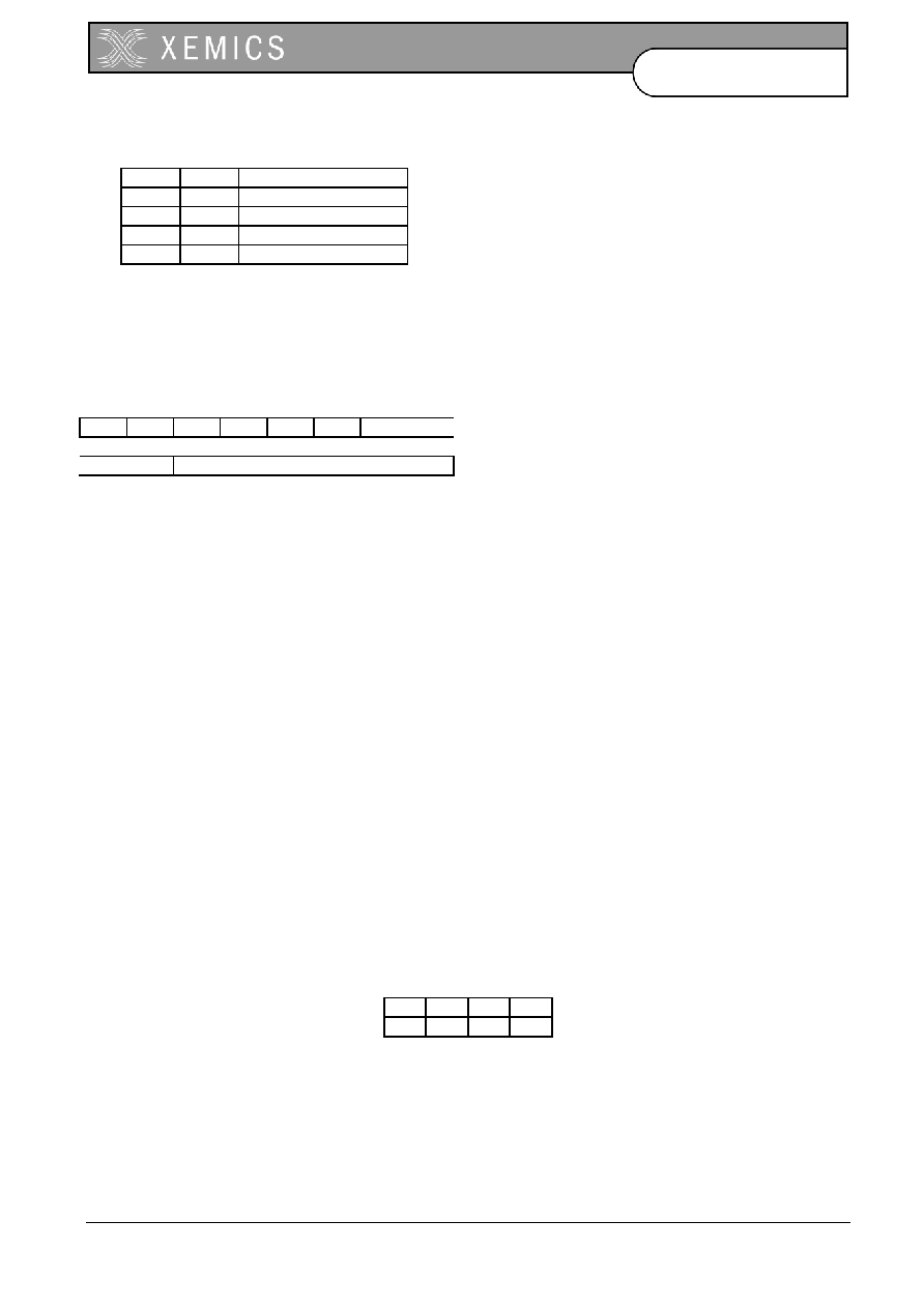
3-wire Bus Data Format
The first two bits (D15 and D14) determine the A, B or C register access according to the truth table below
(table 1).
D15 D14 REGISTER
NAME
0 0 REGISTER
A
0 1 REGISTER
B
1 0 REGISTER
C
1 1 NOT
USED
table 1: Register Address
These three registers are filled by the data A13 to A0, B13 to B0 or C13 to C0 according to the value of D15
and D14. Register A is used to set the XE1201A mode (transmission, reception and standby modes) and to
select the receiver data rate. Register B is used for central frequency adjustment during transmission.
Register C is used for frequency deviation set-up, transmitted power adjustment and other auxiliary functions.
"A" REGISTER FORMAT (D15=0, D14=0)
D15 D14 A13 A12 A11 A10 A9 A8
A7 A6 A5 A4 A3 A2 A1 A0
table 2: "A" Register Format
A13 - CONTROL MODE BIT
When set to 0, this bit enables the XE1201A transmit/receive mode and chip enable control to be addressed
via the pin15 (RXTX) and pin1 (EN). For further information on this control mode, please refer to RXTX pin
and EN pin description on page 7. When set to 1, the transmit/receive mode and chip enable controls are
addressed by bit A10 and A11. In this mode, the levels applied on pin 15 and pin 1 have no effect.
A12 - CLOCK CONTROL
This bit is used for XE1201A internal clock start-up. When set to 1, the clock is always running whatever the
state of the chip enable bit (A11 when A13=1 or pin1 when A13=0). When set to 0, the clock activity is
determined by the chip enable bit (A11).
A11 - CHIP ENABLE
When set to 0, all the blocks of XE1201A are deactivated (except the clock if the bit A12 is set to 1). However,
the 3-wire bus can be programmed in disabled mode as long as Vdd is present. This bit replaces the Chip
Enable (pin1) when A13=1.
A10 - TRANSMIT/RECEIVE MODE
When set to 1, the XE1201A is set in receiving mode and in transmitting mode when set to 0. This bit replaces
the RXTX (pin15) when A13=1
A9, A8, A7, A6 ≠ DEMODULATOR AND BIT SYNCHRONIZER BYPASSING
These bits are used in applications where the bit synchronizer is not needed for e.g. decrease the receiver
wake-up time
a) The receiver is in normal mode but the demodulator is bypassed. The outputs I and Q of the limiters are
available on pin19
(I output) and pin 18 (Q output). Bits A9 to A6 must be set according to table 3 below.
A9 A8 A7 A6
0 1 0 0
table 3: Receiver Mode with Demodulator Bypassed
5 D0205-118