Cool Solutions for Wireless Connectivity
XEMICS SA
∑
e-mail: info@xemics.com
∑
web: www.xemics.com
Datasheet
XE1203
L N A
F A M P
P H A S E
S H I F T E R
L O _ B U F
M M O D
D IV ID E R
V C O
P A
C H P U M P
P F D
I R E F
F A M P
R F O U T
T K A
T K B
L F B
R F A
R F B
D IV C T L
V C O
T A N K
L O O P
F I L T E R
M A T C H I N G
N E T W O R K
M A T C H I N G
N E T W O R K
V
DDF
VDD
D
V
DDP
VS
SF
VS
SD
V
SSP
L P F
L P F
B B A M P
L IM
L I M
O S C IL L A T O R
/ n
C L O C K O U T
D E M O D
P A T T E R N
M A T C H IN G
B B A M P
P O R
I R E F
m o d u la to r
/ n
S y n t h e s iz e r
F E I
B I T S Y N C
X T A
X T B
C L K O U T
T S U P P T M O D ( 3 : 0 )
P O R
C L K X T A L
VDD
V
DDA
VS
S
VS
SA
X T A L
1 1 B its
B A R K E R
D E C O D E R
P A T T E R N
S I
D C L K
D A T A
D A T A I N
X E 1 2 0 3
L O G IC
C O N T R O L
1 1 B it s
B A R K E R
E N C O D E R
R S S I
C O N T R O L
D A T A
S O
S C K
E N
S W I T C H
XE1203
433MHz / 868MHz / 915MHz
Low-power, integrated UHF transceiver
GENERAL DESCRIPTION
The XE1203 is a single chip transceiver operating
in the 868 and 915MHz license-free ISM (Industry
Scientific and Medical) frequency bands. Its highly
integrated architecture allows for minimum
external components while maintaining design
flexibility. All major RF communication parameters
are programmable and most of them can be
dynamically set. The XE1203 offers the unique
advantage of high data rate communication at
rates up to 152.3kbit/s, without the need to modify
the number or parameters of the external
components. The XE1203 is optimized for low
power consumption while offering high RF output
power and exceptional receiver sensitivity. The
device is suitable for circuit applications which
have to satisfy either the European (ETSI-300-
220) or the North American (FCC part 15)
regulatory standards.
APPLICATIONS
∑
Automated Meter Reading (AMR)
∑
Home Automation and Access Control
∑
High-Quality Speech, Music and Data over RF
∑
Applications requiring Konnex-compatibility
KEY PRODUCT FEATURES
∑
RF output power: up to +15dBm on a 50
load (typical)
∑
High reception sensitivity: down to ≠113 dBm
(typical)
∑
Low power consumption:
R
X
= 14mA; T
X
= 62 mA @15dBm (typical)
∑
Supply voltage down to 2.4V
∑
Data rate from 1.2 to 152.3kbps, NRZ coding
∑
Konnex-compatible operation mode
∑
11-bit Barker encoder/decoder
∑
On-chip frequency synthesizer with steps of
500Hz
∑
Continuous phase 2-level FSK modulation
∑
Received data pattern recognition (for wake-
up)
∑
Bit-Synchronizer for incoming data/clock
synchronization and recovery
∑
RSSI (Received Signal Strength Indicator)
∑
FEI (Frequency Error Indicator)
ORDERING INFORMATION
Part number Temperature range Package
XE1203I063
-40∞C to +85∞
VQFN48

2
D0308-214
Data Sheet
XE1203
Table of Contents
1
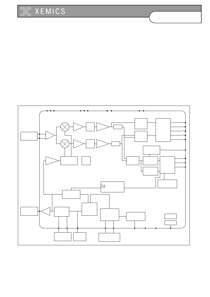
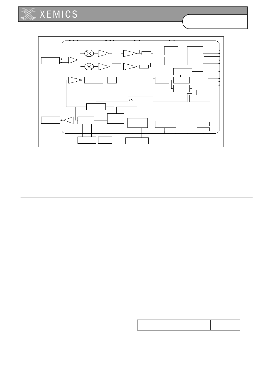
Functional Block Diagram .........................................................................................................................3
2
Pin description............................................................................................................................................4
3
Electrical Characteristics...........................................................................................................................5
3.1
Absolute Maximum Operating Ranges.........................................................................................................5
3.2
Specifications................................................................................................................................................5
3.2.1
Operating Range ...........................................................................................................................................5
3.2.2
Electrical Specifications ................................................................................................................................6
4
General Description....................................................................................................................................8
4.1
Detailed description ......................................................................................................................................8
4.1.1
Introduction....................................................................................................................................................8
4.1.2
Receiver ........................................................................................................................................................8
4.1.3
Demodulation chain ......................................................................................................................................9
4.1.4
The demodulator, ..........................................................................................................................................9
4.1.5
The bit synchronizer....................................................................................................................................10
4.1.6
The barker decoder,....................................................................................................................................11
4.1.7
Pattern recognition block.............................................................................................................................12
4.1.8
High sensitivity vs. high linearity: A-mode, B-mode ....................................................................................13
4.1.9
RSSI ............................................................................................................................................................13
4.1.10Frequency Error Indicator - FEI...................................................................................................................14
4.1.11Transmitter ..................................................................................................................................................15
4.1.12Barker encoding. .........................................................................................................................................17
4.1.13Clock Output for external processor............................................................................................................18
5
Interface definition, Principles of operation ..........................................................................................19
5.1
Serial Control Interface...............................................................................................................................19
5.2
Configuration and Status registers .............................................................................................................20
5.2.1
Configuration register: general description .................................................................................................21
5.2.2
RTParam configuration register ..................................................................................................................22
5.2.3
FSParam configuration register ..................................................................................................................24
5.2.4
Switching parameters..................................................................................................................................25
5.2.5
DataOut register ..........................................................................................................................................26
5.2.6
ADParam configuration register ..................................................................................................................27
5.2.7
Pattern register............................................................................................................................................29
5.3
Operating Modes ........................................................................................................................................30
5.3.1
Standard power up sequence for the receiver and transmitter...................................................................31
5.4
Selection of the reference frequency..........................................................................................................32
5.5
Clock Output Interface................................................................................................................................32
5.6
Default settings at power-up.......................................................................................................................32
6
Application Information ...........................................................................................................................33
6.1
Matching network of the receiver................................................................................................................33
6.2
Matching network of the transmitter ...........................................................................................................33
6.3
VCO tank ....................................................................................................................................................34
6.4
Loop filter of the frequency synthesizer......................................................................................................34
6.5
Reference crystal for the frequency synthesizer ........................................................................................35
6.6
Typical application ......................................................................................................................................36
7
Packaging information.............................................................................................................................37
4
D0308-214
Data Sheet
XE1203
2 PIN
DESCRIPTION
PIN
NAME
I/O
Description
36
VDD
IN
VDD for low frequency digital blocks
18
VDDD
IN
VDD for high frequency digital blocks
29
VDDA
IN
VDD for low frequency analog blocks
12
VDDF
IN
VDD for high frequency analog blocks
10
VDDP
IN
VDD for the power amplifier
42
VSS
IN
VSS for low frequency digital blocks
19
VSSD
IN
VSS for high frequency digital blocks
27,25
VSSA
IN
VSS for low frequency analog blocks
4,16,13
VSSF
IN
VSS for high frequency analog blocks
7,8
VSSP
IN
VSS for the power amplifier
5 RFA
IN
RF
input
6 RFB
IN
RF
input
9 RFOUT
OUT
RF
output
14 TKA
IN/OUT
VCO
tank
15 TKB
IN/OUT
VCO
tank
17
LFB
IN/OUT Loop filter of the PLL
26
XTA
IN/OUT Quartz and input of external clock
28 XTB
IN/OUT
Quartz
1,2,3,22,30,31,47,48
Not
connected
39
SI
IN
Data input of the 3-wires interface
35
EN
IN
3-wire interface communication enable signal
38
SO
OUT
Data output of the 3-wires interface
40
SCK
IN
Input clock of the 3-wires interface
37
SWITCH
IN/OUT Receiver or Transmitter mode selection
43
DCLK
OUT
Transmitter or Receiver clock
45
DATAIN
IN
Transmitter input data
44 DATA
IN/OUT
Transmitter
input
data or Receiver output data
41
CLKOUT
Out
Output clock at quartz frequency divided by 4, 8, 16 or 32
46
PATTERN
Out
Output of the pattern recognition block
11,20,21,23,24,32,
33, 34
Test pins
IN
Connected to ground