Document Outline
- GENERAL DESCRIPTION
- KEY FEATURES
- APPLICATIONS
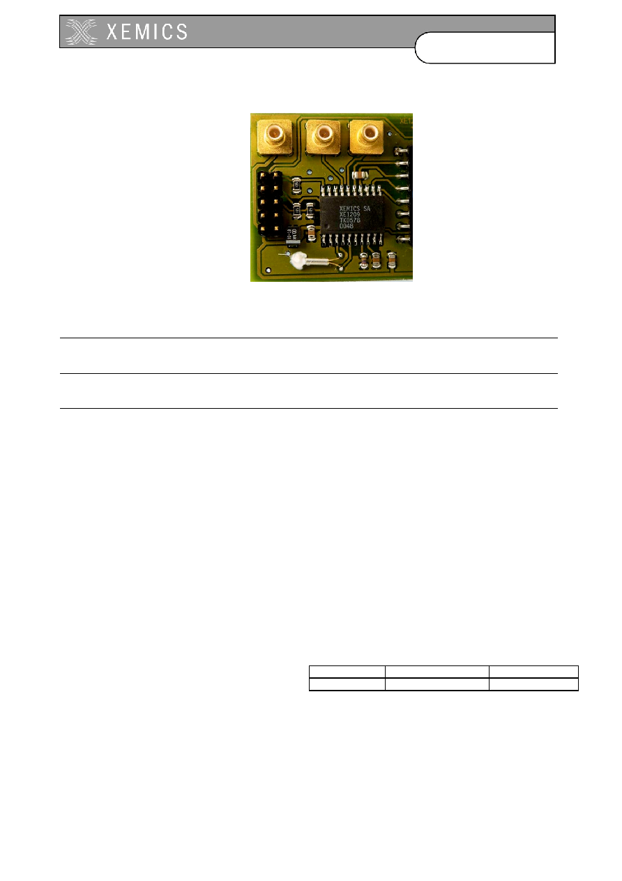
- ORDERING INFORMATION
- PIN DESCRIPTION
- TYPICAL APPLICATION
- Typical external components
- GENERAL FUNCTIONAL DESCRIPTION
- ABSOLUTE MAXIMUM RATINGS, OPERATING RANGES AND EXTERNAL CONDITIONS
- ELECTRICAL SPECIFICATIONS
- INPUT/OUTPUT RF SIGNALS
- PROGRAMMING / DATA INTERFACE
Datasheet XE1209
Ultra Low Power CMOS
Transceiver
Cool Solutions for Wireless Connectivit y
XEMICS SA
∑
e-mail: info@xemics.com
∑
web: www.xemics.com
XE1209 30 ≠ 70 kHz
Ultra Low Power CMOS Transceiver
G
ENERAL
D
ESCRIPTION
The XE1209 is a CMOS Ultra Low-Power
transceiver for short-range low frequency RF
data communications system. It uses 2-level
Continuous Phase FSK modulation. The
receiver section includes the preamplifier, the
down-converter, and the channel filters, the
demodulator and the bit synchronizer, which
delivers synchronized data at the output. The
transmitter section is composed of a Direct
Digital Synthesizer (DDS), and the power
amplifier generating a square-wave output
current. The XE1209 has carrier detector to
detect the presence of a signal at the carrier
frequency. The local clock is based on a 32kHz
crystal oscillator and a PLL to generate the
required Local oscillator (LO) frequency. The
XE1209 has a simple interface with an external
microcontroller.
K
EY
F
EATURES
∑
Single chip transceiver
∑
Low cost
∑
Low external component count
∑
Ultra Low Power
- Stand-by
mode
-
Carrier detection mode
-
Low-power receiver mode
∑
Unlicensed frequency band
∑
Short range applications; 1 to 3 meters
A
PPLICATIONS
∑
Remote control
∑
Short Range Wireless data
∑
Access control
O
RDERING INFORMATION
Part number
Temperature range
Package
XE1209C012
-10∞C to +60∞
SO20

2
D0205-51
Datasheet XE1209
Ultra Low Power CMOS
Transceiver
P
IN DESCRIPTION
Pin #
Name
Description
1
TEST
Test pin
2
VSS
Ground for digital
3
QIN
Xtal pin or input for external clock
4
VDDA
Supply voltage for analog
5
QOUT
Xtal pin
6
VSSA
Ground for analog
7
IREF
Iref node for external resistance
8
VREF
Vref node for external capacitance
9
SUPTEST
Test pin
10
RE
Receiver enable
11
INA
RF input signal
12
INB
RF input signal
13
VSSPA
Ground for RF power amplifier
14
PAOUT
RF power amplifier output
15
VDD
Supply voltage for digital
16
DCLK
Received data clock output
17
DATA
Input/output bit stream or output of the carrier detector
18
DE
Data enable for 3-wire communication
19
SD
Data input for 3-wire communication
20
SC
Clock input for 3-wire communication
T
YPICAL
A
PPLICATION
The product is to be used in a system for low frequency RF data communications. The transmission is made
with 2-level CPFSK modulation. The modulated signal has a carrier frequency fc and a deviation frequency
f; the coding of the data is the following:
f
RFin
= fc +
f
"1"
f
RFin
= fc -
f
"0".
The Figure 1 below shows the structure of the transceiver and the external components required by the
application. A 3-wire bus allows the product to receive configuration data from a microcontroller.
Note: pin
TEST remains
unconnected
Figure 1 Application diagram
150k
68m
H
68
m
H
2.2nF
270 pF
270 pF
Vdd
47 nF
280K
100 nF
Riref
Cvref
30uH
Limiter
I
DE
SC
SD
RE
DATA
VDD
VSS
TEST
VREF
QIN
QOUT
VSSPA
PAOUT
INA
INB
IREF
DCLK
SUPTEST
VDDA
VSSA
to MCU
to MCU
100 nF
Vdd
Cvdd
Xtal
to MCU
Limiter
Demodulator
+
Bit
Synchronizer
Power
Management
+
Serial Bus
Interface
XTAL
Oscillator
Progr.
Divider
VCO
Phase
Acc
MSB
Loop
Filter
Sequencer
Current/
Voltage
Ref
Phase/
Frequency
Detector
Progr.
Power
Amp
Low Pass
Filter
Sine
Filter
Low Pass
Filter
Sine
Filter
Carrier
Detector
Preamp

D0205-51
3
Datasheet XE1209
Ultra Low Power CMOS
Transceiver
Typical external components
Besides the components needed for the RF communication itself, the following external components are
required:
Name
Type
Pins to be connected
Value
Tolerance
Max. Temp. variation
Cvdd
Capacitor
VDD - VSS
100 nF
±
10 %
±
5 % over -10 ∞C to 60 ∞C
Cvref
Capacitor
VREF - VSS
47 nF
±
10 %
±
5 % over -10 ∞C to 60 ∞C
Riref
Resistance
IREF - VSS
280 k
±
1 %
±
100 ppm/K
Xtal
Crystal
QIN - QOUT
32.768 kHz
±
20 ppm
- 50 ppm over -10 to 60 ∞C
The reference of the crystal used for Xtal is the following:
"DS26 watch crystal" from Micro Crystal Switzerland
G
ENERAL
F
UNCTIONAL
D
ESCRIPTION
The XE1209 is composed of 6 main functional blocks:
Receiver
The receiver channel converts a 2-level CPFSK modulated signal into a bit stream. It is composed of the
following blocks: preamplifier, down-converters (0-IF architecture), channel filters, limiters, demodulator, and
bit synchronizer.
Transmitter
The transmitter performs the modulation of an input bit-stream. The main parts of this block are a DDS
(Direct Digital Synthesizer), generating a digital signal with a modulated period, and a power amplifier
generating a square-wave output current controlled by the output of the DDS.
Carrier detector
The function of this block is to detect the presence of a signal at the carrier frequency fc.
Clock generator
The clock generator is composed of a quartz oscillator generating the reference signal at 32.768 kHz, and a
PLL (Phase Locked Loop), whose function is to deliver a signal at a frequency which is a multiple of the
oscillator output; the multiplying factor is programmable on two values.
Service block
This block provides the whole circuit with the required voltage references and current sources.
Digital part
The digital part has two main functions:
∑
implement the 3-wire interface for the communication with the external microcontroller.
∑
generate all the internal signals according to the selected mode of operation and the content of the
configuration register
The product has four operating modes:
∑
a standby mode (M1), where all the blocks are powered off (in this mode, the oscillator can be either on or off
according to the value of a bit (called OSC) stored in the configuration register),
∑
a carrier detector mode (M2), where only the carrier detector is active,
∑
a transmitter mode (M3), where the transmitter is powered on,
∑
A receiver mode (M4), where the receiver is powered on.

D0205-51
4
Datasheet XE1209
Ultra Low Power CMOS
Transceiver
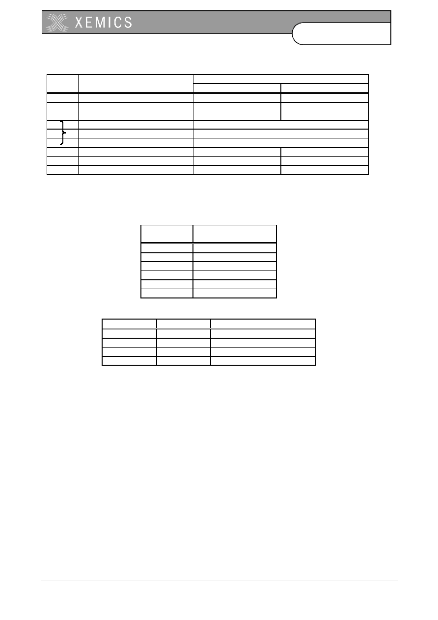
The RE input and the bit TR in the configuration register determine the mode setting. The Table 1 gives the status
of the main blocks in each mode.
M1
standby
M2
carrier
detection
M3
Tx
M4
Rx
Receiver
off
off
off
ON
Transmitter
off
off
ON
off
Carrier
detector
off
ON
off
off
Clock
Osc
ON/off
ON / off
ON / off
ON / off
generator
PLL
off
off
ON
ON
Service
block
off
ON
ON
ON
Digital part
ON
ON
ON
ON
Table 1 Mode selection
When the oscillator is off (bit OSC=0), an external clock is applied on the pin QIN.
A
BSOLUTE
M
AXIMUM
R
ATINGS
, O
PERATING RANGES AND EXTERNAL CONDITIONS
Symb
Parameters
Conditions
Min
Typ
Max
Unit
STO_TR
Storage temperature
range
-40
-
+85
∞C
TR
Operating temperature
range
-10
+25
+60
∞C
VDD
Operating supply
voltage
2.0
2.6
3.2
V
FREF_EXT
PLL reference
frequency
External oscillator,
VDD=2.6 V, temp=25 ∞C
32.735
32.768
32.800
kHz
CL_CK
External capacitate
load on the pin CLK
Full range of supply and
temperature
-
-
5
pF
IL_CK
External leakage
current on the pin CLK
Full range of supply and
temperature
-
-
50
nA
RP_OSC
Parasitic resistance
between the pins QIN,
QOUT and any other
ASIC pin
Full range of supply and
temperature
20
-
-
M
CP_OSC
Parasitic capacitance
between the pins QIN,
QOUT and any other
ASIC pin
Full range of supply and
temperature
-
-
0.5
pF
Stresses above those listed in this clause may cause permanent device failure. Exposure to absolute
maximum ratings for extended periods may affect device reliability.
Electrostatic discharges:
∑
The device withstands 2000 Volts Standardized Human Body Model ESD pulses when tested according
to MIL883C method 3015.5 (pin combination 2).
Latch-up:
∑
Static latch-up protection level is 30mA at 25 C
D0205-51
5
Datasheet XE1209
Ultra Low Power CMOS
Transceiver
E
LECTRICAL SPECIFICATIONS
Electrical specifications are defined for VDD=2.6 V, Temp=25 ∞C, fc=36.86 kHz, and a data rate of 1820
bit/s, unless otherwise specified.
Symb
Parameters
Conditions
Min
Typ
Max
Unit
IDDS1
Standby current
Oscillator stopped
-
0.15
1
µA
IDDS2
Standby current
Oscillator active,
VDD=3V, Temp= -10 to
+60∞C, unloaded
-
1
2
µA
IDD1
Supply current in carrier
detection mode (M2)
Temp = -10 to +60 ∞C
-
95
120
µA
IDD2
Supply current in receiver
mode (M4)
Temp = -10 to +60 ∞C
-
200
300
µA
ISINK
Sink current transmitter
mode (peak value)
Load = resistance of 15
ohms connected between
VDD and pin PAOUT,
programmable through
the 3-wire bus
82
45
23
5.65
2.60
1.35
110
60
30
7.5
3.5
1.80
138
75
37
9.35
4.40
2.25
mA
mA
mA
mA
mA
mA
FREF
PLL reference frequency
-
32.768
-
kHz
FR
PLL frequency
Programmable via 3-wire
bus
588.65
719.45
589.82
720.90
591.00
722.35
kHz
kHz
RIN
RF differential input DC
resistance
500
1000
-
k
CIN
RF differential input
capacitance
-
25
-
pF
RFS
RF sensitivity
Rsource=100
BER=10
-4
200
70
-
µVp
MAXIN Maximum RF effective
input signal
Without any parasitic
signal
-
-
15
mV
FC
Transmission carrier
frequency
-
-
36.86
45.05
-
-
kHz
kHz
ATT
Adjacent channel
rejection at f = 30.6 kHz
At RFSmin
Rsource=100
,BER=10
-4
11
23
-
dBc
ATT3
Adjacent channel
rejection at f = 110.58 kHz
At RFSmin
Rsource=100
,BER=10
-4
-1
3
-
dBc
CMRR
DC
DC Common mode
rejection ratio
At RFSmin
Rsource=100
,BER=10
-4
30
-
-
dB
BW
Receiver -3dB Bandwidth
FC=36.86 kHz, DSB
-
5000
-
Hz
DR
Data rate
-
1820
-
bit/s
FDEV
Frequency deviation
FC=36.86 kHz
-
1872
-
Hz
PDL
Carrier detector level
3 rising edges measured
at output in a 900us time
window
140
400
200
500
260
600
µVp
µVp
D0205-51
6
Datasheet XE1209
Ultra Low Power CMOS
Transceiver
Symb
Parameters
Conditions
Min
Typ
Max
Unit
RAC
Receiver Activation time
from
carrier-detector
mode and with oscillator
running
-
1.6
2.5
ms
XOAC
Xtal oscillator activation
time
at temp =-10 to +60∞C
0.2
2
s
LL
Logical low level
VSS
-
0.2*VDD
V
HL
Logical high level
0.8*VDD
-
VDD
V
I
NPUT
/O
UTPUT
RF S
IGNALS
Transmit Mode
The transmitter is composed of a DDS and a power amplifier. The DDS is a 12-bits counter, which is
incremented by 256+13 when the input data is 1 and by 256-13 when the input data is 0. This way, the
frequency deviation is equal to:
f
N FREF
=
13
2
12
,
Where N is the multiplying factor of the PLL, and FREF the frequency of the reference clock. With N=18 and
FREF=32.768 kHz, the expression gives f=1872 Hz.
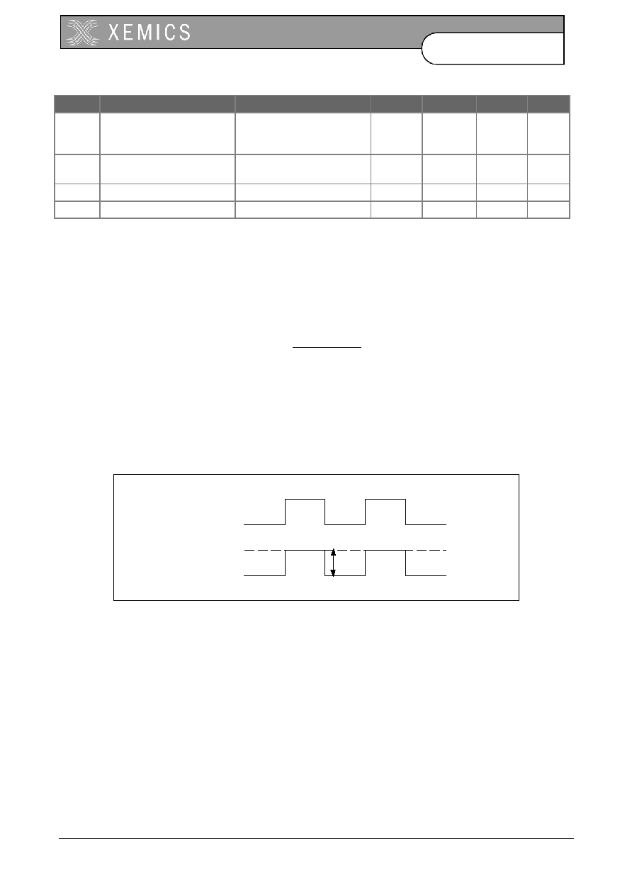
The power amplifier delivers a square wave current whose amplitude is programmable (see the configuration
register section below). The figure below shows the shapes of the signals when, as an example, ISINK=110
mA. The transmitter processes the input data in real time without any additional sampling or filtering, which
means that the data rate does not depend on the XE1209.
DDS output
PA sink current
110 mA
0 mA
ISINK

D0205-51
7
Datasheet XE1209
Ultra Low Power CMOS
Transceiver
Receive Mode
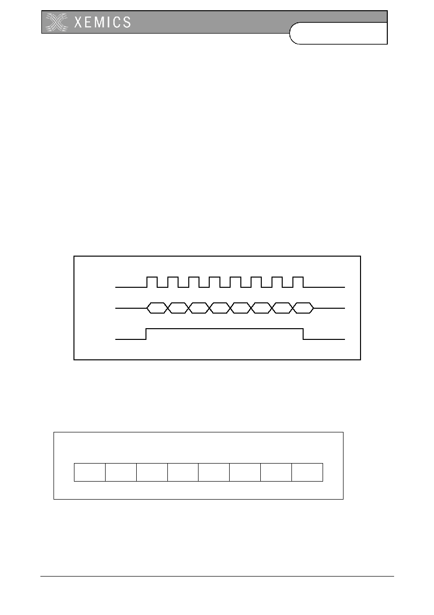
The data available at receiver output are valid between 20% and 60% of the data period (1/DR) after the
rising edge of the clock (DCLK) as shown in figure below. The received data rate must be 1820 bit/s +/- 2 %
for proper bit synchronizer operation. In addition, the bit synchronizer needs to see at least one transition
(from "1" to "0" or from "0" to "1") every 8 bits present at its input.
At the beginning of the reception, the bit synchronizer needs to receive a preamble which is a sequence of
16 "0" and "1" bit sent alternatively.
Carrier Detection Mode
The Carrier Detection mode is active when the TR bit in the configuration register is 0 and the RE input pin is
1. The signal present at RF inputs is amplified and compared to a voltage threshold. When a RF signal is
present at the input, the comparator output is a square wave at a frequency equal to the frequency of the RF
signal. This signal is fed into a 3-bit counter, whose output is directly available on the DATA pin. In this case,
the DATA signal is a square wave whose frequency is 1/8 of the RF carrier frequency.
20% of 1/DR
60% of 1/DR
1/DR
DATA
DCLK
RE
(TR=0)
RFIN
(shown as
square wave)
~ 4.8 ms
DATA
RE
(TR=0)
RFIN
(shown as
square wave)
~ 4.8 ms
DATA
D0205-51
8
Datasheet XE1209
Ultra Low Power CMOS
Transceiver
The carrier detector set-up time (after TR bit set to 0 and RE input set to 1) is 4.85ms when the carrier
frequency is 36.86 kHz. In the applications where the carrier detector is turned on for a relative long period
(tens to hundreds of ms), it is recommended to reset the block with a short transition to stand-by mode
(RE=0).
The timing diagram of the carrier detection is shown below when a RF signal is present at input and the
function is programmed
P
ROGRAMMING
/ D
ATA
I
NTERFACE
Programming the XE1209 is performed through the 3-wire interface SC, SD, DE, as shown below.
The enable signal DE goes low at the same time as the 8th falling edge of SC (that is, with a maximum delay
between each other of 100 ns). From the rising edge of DE, the XE1209 will sample the data present on SD at
the first 8 falling edges of SC, whatever is the following sequence on SC and SD. For a proper data transfer, the
data on SD must be stable for 5 microseconds before and after each falling edge on SC.
The values on SC, SD and DE (as well as RE) must be kept constant (either at VDD or VSS) during all the
time where the XE1209 has to be effective in modes M2, M3 and M4.
SC
SD
DE
R0
R3
R2
R1
R6
R5
R4
R7
Configuration Register
The content of the configuration register is described below. The bit R0 is the first
received data during the 3-wire communication.
TEST
SENS
OSC
P2
P0
TR
P1
FC
R0
R1
R2
R3
R4
R5
R6
R7
D0205-51
9
Datasheet XE1209
Ultra Low Power CMOS
Transceiver
Name
Description
Convention
0
1
FC
Carrier frequency
36.86 kHz
45.05 kHz
TR
Transmission flag
Mode M1 (RE=0)
Mode M2 (RE=1)
Mode M3 (RE=0)
Mode M4 (RE=1)
P0
Power level
LSB
P1
Power level
(see Table 3)
P2
Power level
MSB
SENS
Carrier detector threshold
200 µV
500 µV
TEST
Test flag
Normal mode
Test mode
OSC
Oscillator flag
External oscillator
Internal oscillator
Table 2 Configuration register
Correspondence between the word {P2 P1 P0} and the current sinked by the power amplifier is shown
below. The words 110 and 111 are reserved for test purposes.
P2 P1 P0
Power amplifier
current
0 0 0
1.8 mA
0 0 1
3.5 mA
0 1 0
7.5 mA
0 1 1
30 mA
1 0 0
60 mA
1 0 1
110 mA
Table 3 Sink current levels
TR (register)
RE (input pin)
Mode
0
0
M1 (standby)
0
1
M2 (carrier detector)
1
0
M3 (transmitter)
1
1
M4 (receiver)
Table 4 Mode selection
Upon start-up, a reset of the XE1209 is required to set the configuration register in a proper default
mode. This is done by sending the binary word 'b00000000 to the circuit using the 3-wire bus, while
setting RE to "0".
XEMICS 2002
All rights reserved. Reproduction in whole or in part is prohibited without the prior written consent of the copyright
owner. The information presented in this document does not form part of any quotation or contract, is believed to be
accurate and reliable and may be changed without notice. No liability will be accepted by the publisher for any
consequence of its use. Publication thereof does not convey nor imply any license under patent or other industrial or
intellectual property rights.
XEMICS PRODUCTS ARE NOT DESIGNED, INTENDED, AUTHORIZED OR WARRANTED TO BE SUITABLE FOR
USE IN LIFE-SUPPORT APPLICATIONS, DEVICES OR SYSTEMS OR OTHER CRITICAL APPLICATIONS.
INCLUSION OF XEMICS PRODUCTS IN SUCH APPLICATIONS IS UNDERSTOOD TO BE UNDERTAKEN
SOLELY AT THE CUSTOMER'S OWN RISK.
Should a customer purchase or use XEMICS products for any such unauthorized application, the customer shall
indemnify and hold XEMICS and its officers, employees, subsidiaries, affiliates, and distributors harmless against all
claims, costs damages and attorney fees which could arise.