 | –≠–ª–µ–∫—Ç—Ä–æ–Ω–Ω—ã–π –∫–æ–º–ø–æ–Ω–µ–Ω—Ç: XE3004 | –°–∫–∞—á–∞—Ç—å:  PDF PDF  ZIP ZIP |
Document Outline
- Table of contents
- 1 Device Description
- 2 Functional Description
- 3 Serial Communications
- 4 Specifications
- 5 Application Information
- 6 Register Description
- 7 Mechanical Information
Cool Solutions for Wireless Connectivity
XEMICS SA
∑
e-mail: info@xemics.com
∑
web: www.xemics.com
Data Sheet
XE3004
XE3004
Low-Power DAC
General Description
The XE3004 is an ultra low-power Digital to Analog
Converter for voice and audio applications. It
includes a 16-bit DAC, serial audio interface,
power management and clock management.
The sampling frequency of the DAC can be
adjusted from 4 kHz to 48 kHz.
Applications
∑
Wireless
speakers
∑
Digital audio playback
∑
Consumer
electronics
∑
Multimedia
applications
∑
Battery-operated portable audio devices
Features
∑
Ultra low-power consumption, below 2 mW
∑
Low-voltage operation down to 1.8 V
∑
Single supply voltage
∑
Adjustable sampling frequency: 4 ≠ 48 kHz
∑
Digital format: 16 bit 2s complement
∑
Easy interfacing to various DSPs
∑
Direct connection to speaker
∑
Various programming options
Quick Reference Data
∑
Supply voltage
1.8 ≠ 3.6 V
∑
Typ. current (@1.8V, f
s
=20 kHz) 65 µA
∑
Sampling frequency
4 ≠ 48 kHz
∑
Typical dynamic range DAC
78 dB
Ordering Information
Part
Package
Temperature range
XE3004
TSSOP 16 pins
-20 to 70
∞
C
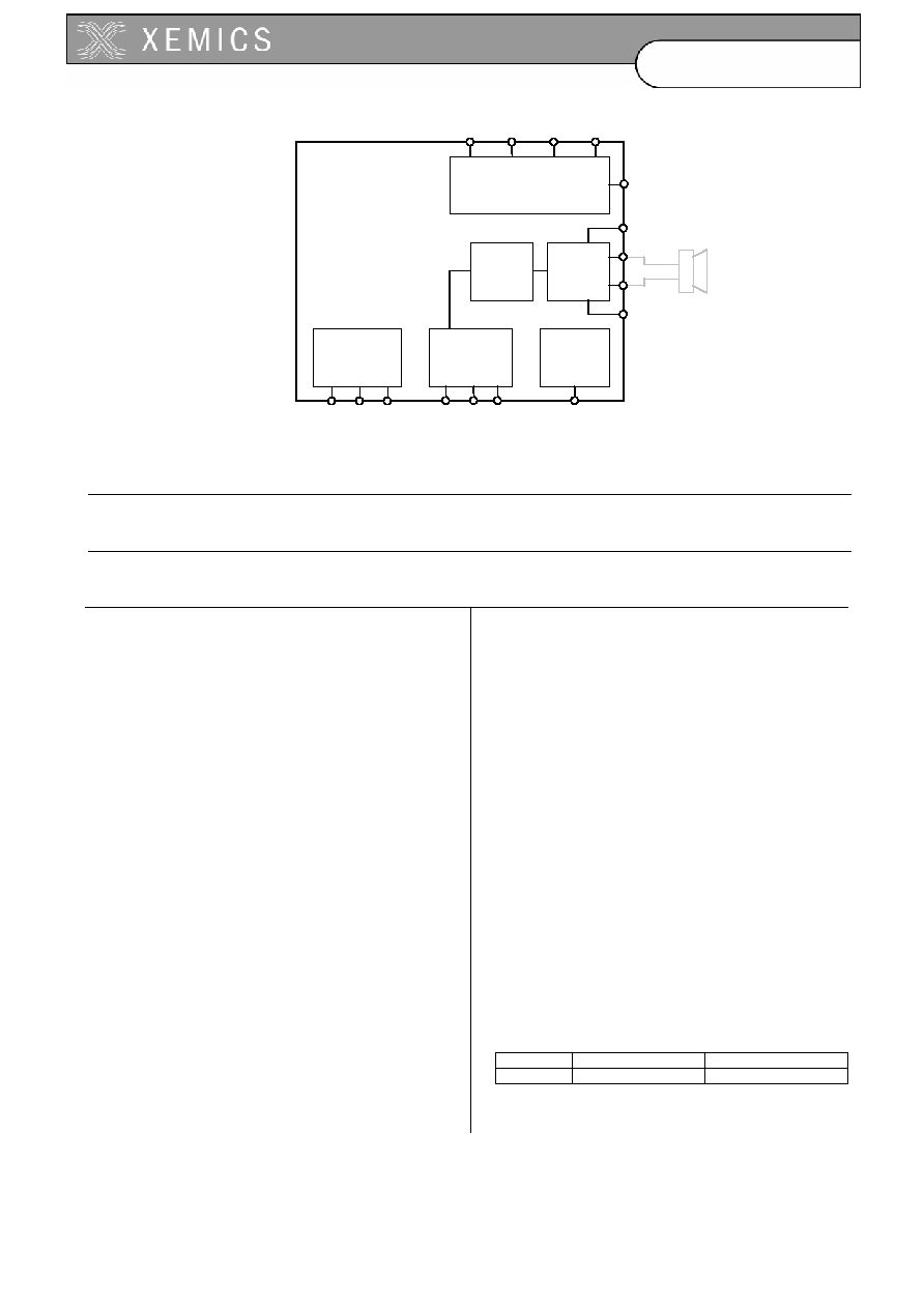
Serial Audio
Interface
SPI
XE3004
Power supply
management
VSSA
VSSD
VDD
MCLK
BCLK
FSYNC
SDI
SCK
SS
VSSA
Clock
mgt
PWM
DAC
Power
amplifier
AOUTP
AOUTN
VDDPA
VSSPA
MOSI
RESET

2
D0311-143
Data Sheet
XE3004
Table of contents
1
Device Description .........................................................................................................................................3
1.1
Terminal Description - XE3004...................................................................................................................3
2
Functional Description...................................................................................................................................4
2.1
Device Functions ........................................................................................................................................5
2.2
Power-Down Functions...............................................................................................................................8
3
Serial Communications..................................................................................................................................9
3.1
Serial Audio Interface..................................................................................................................................9
3.2
Register Programming..............................................................................................................................10
3.3
Serial Peripheral Interface - SPI ...............................................................................................................11
4
Specifications ...............................................................................................................................................13
4.1
Absolute Maximum Ratings ......................................................................................................................13
4.2
Recommended Operating Conditions ......................................................................................................13
4.3
Electrical Characteristics ..........................................................................................................................14
5
Application Information ...............................................................................................................................19
5.1
Application Schematics ≠ XE3004............................................................................................................19
6
Register Description ....................................................................................................................................20
6.1
Register Functional Summary ..................................................................................................................20
6.2
Register Definitions...................................................................................................................................20
7
Mechanical Information ...............................................................................................................................22
3
D0311-143
Data Sheet
XE3004
1 Device
Description
1
5
6
7
8
MCLK
SS
NRESET
VSSA
VSSD
16
15
14
13
12
11
10
9
MOSI
VDD
SCK
SDI
BCLK
FSYNC
AOUTN
4
3
2
VSSA
VSSPA
AOUTP
VDDPA
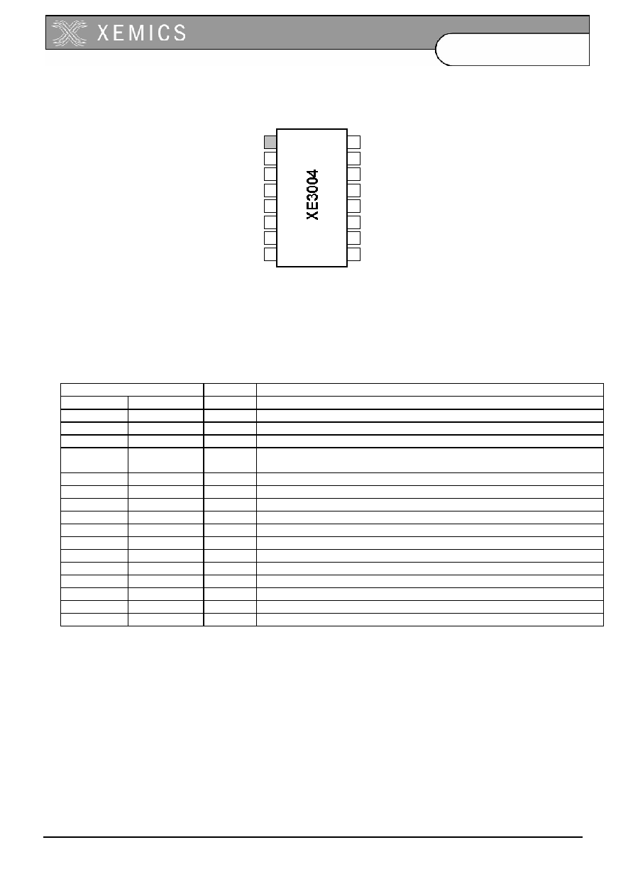
Figure 1: Pin layout of the XE3004
The XE3004 is available in a TSSOP16 package. Detailed information is found in chapter 7, Mechanical
Information.
1.1 Terminal Description - XE3004
Terminals Type
1
Description
XE3004 Name
1
MCLK
DI
Master Clock. MCLK derives the internal DAC clock
2
SS
DI PU
SPI Slave Select
3
VDD
AI
Digital power supply
4
NRESET ZI/O
Reset signal generated by the DAC. If required, the reset signal can be
applied externally to initialize all the internal DAC registers
5 VSSA
AI
Analog
ground
6 VSSA
AI
Analog
ground
7 VSSD
AI
Digital
ground
8
VSSPA
AI
DAC Power Amplifier Ground
9
AOUTN
AO
DAC Analog Output negative
10
VDDPA
AI
DAC Power Amplifier Supply
11
AOUTP
AO
DAC Analog Output positive
12
FSYNC
DI/O
Serial audio interface Frame Synchronization
13
BCLK
DI/O
Serial audio interface Bit Clock
14
SDI
DI PD
Serial audio interface Data Input
15
SCK
DI PD
SPI Serial Clock
16
MOSI
DI PD
SPI Master Out Slave In
Note: (1)
AI = Analog Input
AO = Analog Output
DI = Digital Input
DO = Digital Output
DI/O = Digital In or Out
ZO = Hi Impedance or Output
PU = internal Pull Up
PD = internal Pull Down
ZI/O = Hi impedance In or Out
4
D0311-143
Data Sheet
XE3004
2 Functional
Description
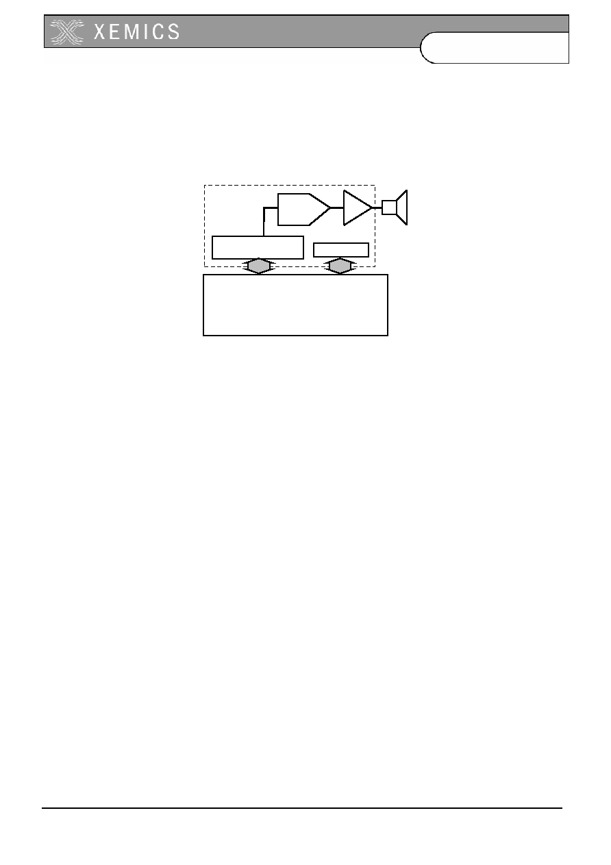
The XE3004 ≠ DAC is typically used as a digital to audio converter for voice and audio applications to interface
between a Digital Signal Processor (DSP) or microcontroller and the analogue interface.
Serial Audio Interface
DAC
DSP / Microcontroller
Digital wireless transmission
Digital audio playback
Power Amplifier
SPI
Figure 2: Typical DAC usage
This chapter provides a brief description of the DAC features. The configuration of the DAC is defined by
programming registers through a serial interface. A detailed description of the registers can be found in chapter 3
and 6. The digital voice and audio samples are passed through the Serial Audio Interface.
5
D0311-143
Data Sheet
XE3004
2.1 Device
Functions
2.1.1 DAC Signal Channel
The DAC is based on a multi bit sigma-delta modulator, which operates at a frequency of 8 times the sampling
rate. The outputs of the modulator are 2's complement words of 6 bit. A pulse-width modulator (PWM) converts
the 6 bit words into 2 single bit streams at 256 times the sampling frequency. Finally the 2 bit streams are
supplied to the power amplifier. The Power Amplifier is a Class D amplifier, which offers higher efficiency than the
traditional Class AB topologies. It uses a three-state unbalanced PWM. This means that both channels of the PA
(AOUTP and AOUTN) will not switch at the same time, therefore the outputs are not purely differential (see figure
3 and 4).
From Serial Audio
Interface
P
N
bit streams
@ 256xFsync
XE3004
Interpolator
&
Modulator
dac_in(15:0)
@ Fsync
pwm_in(5:0)
@ 8xFsync
Power
Amplifier
s
s = 1 s = 0
P
N
P
N
VSSPA
VDDPA
Pulse Width
Modulator
AOUTP
AOUTN
Figure 3: DAC block diagram
Figure 4 shows the relation of input and output samples of the PWM (The timing diagram is not to scale in the
time-axis).
pwm_in(5:0) = -1
P
N
OUTP-OUTN
1/(256 x Fsync)
2/(256 x Fsync)
pwm_in(5:0) = 1
pwm_in(5:0) = 0
pwm_in(5:0) = 2
1/(8 x Fsync)
1
0
1
0
VDDPA
VSSPA
-VDDPA
1/(256 x Fsync)
Figure 4: examples PWM in and out (not to scale)
The DAC receives 16-bit wide 2's complement format through the Serial Audio Interface. The protocol can be
selected through register J. The complete DAC and PA amplifier chain can be powered-down through register I.
6
D0311-143
Data Sheet
XE3004
2.1.2 Operating
Frequency
A master clock (MCLK) has to be applied to the DAC. The clock frequency of the signal applied to the MCLK pin
may vary between 1.024 MHz minimum and 33.9 MHz maximum. The maximum internal clock signal frequency
(MCLK/div_factor) should not exceed 12.288 MHz.
The div_factor can be set by the user in register I to 1,2 or 4. The default value for div_factor is `1'.
2.1.3 Serial Audio Interface
The Serial Audio Interface is a 3-wire interface. It operates on the bit serial clock BCLK and the frame
synchronization signal FSYNC. The sampling frequency of the DAC corresponds to the rate at which the Audio
Serial Interface will put out succeeding frames. One frame always corresponds to one sample. One frame always
contains 2 channels.
Synchronizing the Serial Audio Interface to the MCLK is recommended. FSYNC and MCLK must have a fixed
ratio as defined by the following relation:
FSYNC = Sampling frequency = frame rate = MCLK/(256 x div_factor).
The pin BCLK defines the time when the data must be presented to the serial audio interface and shifted into (pin
SDI) the DAC. The number of BCLK periods in one FSYNC period is 32. The user can select to use the first 16
clock cycles (channel 1) or the second 16 clock cycles (channel 2) of BLCK to shift in the data samples.
The table below shows some examples of the relationships between MCLK, BCLK and FSYNC
MCLK
Div_factor
BCLK
FSYNC
2048 kHz
1
256 kHz
8 kHz
8192 kHz
4
256 kHz
8 kHz
5120 kHz
1
640 kHz
20 kHz
22579.2 kHz
2
1411.2 kHz
44.1 kHz
The table below shows the possible functional configurations of the serial audio interface
DAC
supported protocol
master
LFS (Long Frame Sync)
slave
LFS, LFS Optimization and SFS (Short Frame Sync)
By default the Serial Audio Interface operates in slave, SFS mode. In slave mode the user needs to generate the
signals BLCK, FSYNC and supply to the DAC.
In master mode the DAC generates the BLCK and FSYNC signals. In that case the BLCK operates at 32 times
the frequency of FSYNC. The DAC master mode can be used with the LFS protocol only.
The register J is used for the different setups of the serial audio interface.
7
D0311-143
Data Sheet
XE3004
2.1.4 Serial Peripheral Interface - SPI
The SPI interface is used to control register values. It is a serial communications interface that is independent of
the rest of the DAC. It allows the device to communicate synchronously with a microprocessor or DSP. The DAC
interface only implements a slave controller. A detailed description can be found in chapter 3, Serial
Communication.
2.1.5 Start-up and Initialization
The DAC generates its own power on reset signal after a power supply is connected to the VDD pin. The reset
signal is made available for the user at the pin NRESET. The rising edge of the NRESET indicates that the
startup sequence of the DAC has finished. In most applications the NRESET pin can be left open.
The NRESET signal generated by the DAC is used to initialize the various blocks in the device and guarantees a
correct start-up of the circuit. The start-up sequence that is automatically carried out upon power-up of the device
is listed below and illustrated in Figure 5.
1) NRESET is low (0V) when the device is not powered and remains low for a short time when VDD (upper
curve in Figure 5) is applied. The low state sustains while VDD, VREF are stabilizing. VERF is an internal
signal only.
2) As soon as the MCLK signal is present, a counter is activated that counts 2
21
periods of the MCLK. After this
moment the NRESET is in the high state (VDD).
1024 ms (MCLK=2.048 kHz)
main reset
NRESET
VDD = 1.8..3.3V
VREF* = 1.2V
time
MCLK
. . .
* internal signal only
t
t
Figure 5: Startup sequence and NRESET signal after power-on.
8
D0311-143
Data Sheet
XE3004
The user can use the NRESET pin in 3 different ways and combinations:
1) Leave the NRESET pin not connected. In this case the DAC will startup as described in figure 10.
2) Use the NRESET pin as an output to indicate, to e.g. a microcontroller, that the DAC finished its power
up Use the NRESET pin to force a re-initialization of the registers to their default values. In this case the
user has to force the NRESET to 0V for at least 32 periods of the MCLK. The circuit which forces the
NRESET to 0V should be able to sink at least 50 µA.
Figure 6 shows the block diagram of the DAC reset.
XE3004
MCLK
NRESET
delay
delay
counter
Power
On
Reset
reset to analog and
digital circuitry of codec
low drive
buffer
Figure 6: DAC reset circuitry
2.2 Power-Down
Functions
2.2.1 Software
Power-Down
Register I allows for the power down of DAC through SPI control. The wake-up time, after powering down the
device is typically 200µs. The maximum standby current is 96µA, depending highly upon the Master clock
(MCLK), see 4.3.3 Power Consumption.
2.2.2 Hardware
Power-Down
The device has no power-down pin. However, by holding down (0 V) the NRESET pin (resetting the device) as
well as the pins MCLK, BCLK and FSYNC, the power consumption will reach the standby current of typically
16µA. Use the standard procedure for power up (see start-up and initialization procedure) after a hardware power
down and apply your registers setup procedure.
9
D0311-143
Data Sheet
XE3004
3 Serial
Communications
3.1 Serial Audio Interface
The Serial Audio Interface is a 3-wire interface for communication of audio data. The 3 terminals are listed below:
∑
BCLK:
Bit serial clock, one clock cycle corresponds to one data bit transmitted or received.
∑
FSYNC:
Frame Synchronization. This signal indicates the start of a data word. The frequency of
the FSYNC corresponds to the sample frequency of the DAC.
∑
SDI:
Serial Data In, data received from external device and sent to DAC.
The clock (BCLK) and synchronization (FSYNC) signals are used for receiving the audio data. The
synchronization signal FSYNC must have a fixed ratio with the master clock signal MCLK.
The Serial Audio Interface supports two formats that are commonly used and that are referred to as SFS (Short
Frame Synchronization) and LFS (Long Frame Synchronization). Data can be received in 2 channels. Which
channel is selected depends on the programmed values in the registers. The two interface protocols are shown
below.
FSYNC
SDI
BCLK
msb lsb
msb
channel 1, sample n
channel 2, no data
channel 1, sample n+1
n
15
n
14
n
0
n+1
15
-
-
-
Figure 7: Audio interface timing LFS mode, channel 1
FSYNC
BCLK
channel 1, sample n
channel 2, sample n
channel 1, sample n+1
SDI
msb
lsb
msb
n
15
n
14
n
0
n+1
15
- -
-
Figure 8: Audio interface timing in SFS mode, channel 1
SDI Data should be changed on the rising edge of BCLK. The SDI data will be read by the DAC on the falling
edge of BLCK. Each rising edge of the FSYNC indicates the start of a new sample.

10
D0311-143
Data Sheet
XE3004
3.1.1 LFS
optimization
For receiving, 32 clock cycles in one frame are always required (figure 7 and 8). This is even the case when only
16 bits have to be received. In most cases this can be easily handled with a DSP and microcontroller.
If the user wants to send a minimum of BLCK cycles, it is possible to shorten channel 1 (channel 2 can not be
shortened).
In the LFS mode, the possibility exists to shorten the number of BLCK cycles to 17 instead of 32. In this case the
data is received in channel 2. Channel 1 is shortened to one BLCK cycle only.
Note! This optimization is possible in slave mode only.
The figure 9 below shows this special LFS mode.
FSYNC
SDI
BCLK
msb
lsb
channel 1, no data
channel 2, sample n
n
15
n
14
n
0
-
msb
channel 2, sample n+1
n
15
n
14
-
channel 1, no data
Figure 9: Audio interface timing in LFS mode,17 BLCK cycles, channel 2
3.2 Register
Programming
The control registers define the configuration of the DAC and define the various modes of operation. During
power-up, all registers will be configured with default values. The control register set consists of 9 registers. A
detailed description is provided chapter 6, Register Description.
The control registers can be changed in the two following ways:
1. Logic values at SPI pins during power-up
There are 3 bits inside the registers which are configured depending on the logic values of the pins SS, SCK and
MOSI during the power up startup sequence as described in chapter 2.1.5
Value at power up
Influenced bits of registers
comments
SS = 1
SS = 0
Register I(0)=0
Register I(0)=1
MCLKDIV division by 1
MCLKDIV division by 2
SCK = 0
SCK = 1
Register J(0)=1
Register J(0)=0
SFS protocol
LFS protocol
MOSI = 0
--
GND
Using the SPI pins at startup the user is able to configure the DAC in the corresponding setups without
reprogramming through the SPI interface and protocol. In best case the SPI interface can then be completely
omitted and the 3 SPI pins can be fixed to `0' or `1'.
11
D0311-143
Data Sheet
XE3004
2. Programming through SPI interface after power-up
Once the device has been powered up, the configuration registers can be modified at all times (also when the
device is active) through the SPI interface.
The following section describes the SPI protocol which is required to change the control registers from their
default values.
3.3 Serial Peripheral Interface - SPI
The serial peripheral interface (SPI) allows the device to communicate synchronously with other devices such as
a microprocessor or a DSP. The DAC interface only implements a slave controller. This section describes the
communication from master (e.g. DSP) to slave (DAC pin MOSI).
Three lines are used to transmit data between the slave and master:
∑
MOSI (Master Out, Slave In) data from master to slave, synchronous with the SPI clock (SCK).
∑
SCK (Serial Clock) synchronizes the data bits of MOSI and MISO.
∑
SS (Slave Select) Slave devices are selected by activating SS.
3.3.1 Protocol
The master puts data on the MOSI line on the falling edge of SCK; the slave reads the data on the rising edge of
SCK. Transmission is by 2 bytes with MSB first.
The SS pin should be kept low during the whole transfer of data.
SS
SCK
MOSI
15
0
14
1
t
disable
1/F
sck
t
recovery
... ...
Figure 10: SPI signal timing
There are three timing constraints:
∑
Recovery time (t
recovery
) between the falling edge of SS and the falling edge of SCK.
∑
Disable time (t
disable
) between the last rising edge of SCK and the rising edge of SS.
∑
SCK frequency (F
SCK
)
Delay
Min
Max
Unit
Comments
t
recover
125
-
ns
t
disable
2 x T
master
- ns
T
master
= clock period of the master clock MCLK
F
SCK
0.5 x F
master
Hz F
master
= frequency of the master clock MCLK
12
D0311-143
Data Sheet
XE3004
3.3.2 SPI Interface Modes
There is only one SPI mode: write.
3.3.2.1 Write
Mode
Write communication always takes place in pairs of bytes. The format of the 2 bytes is:
Bit 7 6 5 4 3 2 1 0
mosi
1
0
0
msb A(4:0) lsb
Bit 7 6 5 4 3 2 1 0
mosi
msb D(7:0) lsb
ss
sck
mosi
request (write to address A(4:0))
write data D(7:0) to address A(4:0)
1
0
0
A4 A2
A
1
A0
A3
msb
lsb
Figure 12: SPI signal timing in write mode
13
D0311-143
Data Sheet
XE3004
4 Specifications
4.1 Absolute Maximum Ratings
Stresses above those listed in the following table may cause permanent failure. Exposure to absolute ratings for
extended periods may affect device reliability.
The values are in accordance with the Absolute Maximum Rating System (IEC 134).
All voltages are referenced to ground (VSSA and VSSD).
Analog and digital grounds are equal (VSSA = VSSD).
Symbol
Parameter
Conditions
Min
Max
Unit
VDD Supply
voltage
-0.3 3.65 V
Tstg Storage
temperature
-65 150 ∞C
TA
Operating free-air temperature, TA
-20
70
∞C
Ves
Electrostatic discharge protection
1)
500
V
Ilus
Static latchup current
2)
10
98
mA
Vlud
Dynamic latchup voltage
2)
50
V
1) Tested according MIL883C Method 3015.6, class JEDEC 1B (Standardized Human Body Model: 100 pF,
1500
, 3 pulses, protection related to substrate).
2) Static and dynamic latchup values are valid at 27 ∞C.
4.2 Recommended Operating Conditions
All voltages referenced to ground (VSSA and VSSD).
Min
Typ
Max
Unit
Supply voltage, VDD
1.8
3.0
3.6
V
Differential output load resistance
16
32
Ohm
Master clock frequency
1.024
33
MHz
DAC conversion rate
20
48
kHz
Operating free-air temperature, TA
-20
70
∞C
14
D0311-143
Data Sheet
XE3004
4.3 Electrical Characteristics
The operating conditions in this section are: VDD = 3.0 V, T = 25∞C.
4.3.1 Digital Inputs and Outputs, FSYNC = 20 kHz, output not loaded
Parameter Test
Conditions
Min Typ Max
Unit
VOH
High-level output voltage, DOUT
IO = -360µA
2.4
VDD+0.5
V
VOL
Low-level output voltage, DOUT
IO = 2mA
VSSD-0.5
0.4
V
IIH
High-level input current, any digital input
VIH = 3.3 V
10
µA
IIL
Low-level input current, any digital input
VIL = 0.6 V
10
µA
Ci Input
capacitance
10 pF
Co Output
capacitance
10 pF
4.3.2 DAC Dynamic Performance, load is an LC filter at 10 kHz
FSYNC = 20 kHz, MCLK = 5 MHz.
Parameter Test
Conditions
Min
Typ
Max
Unit
SNR
Signal-to-noise ratio
Bandwidth 10 kHz
72
78
dB
THD
Total harmonic distortion
º full scale
0.5
%
Dynamic range
Bandwidth 10 kHz
72
78
dB
GD
Group delay
FSYNC = 20 kHz
150
µ
s
15
D0311-143
Data Sheet
XE3004
4.3.3 Power
Consumption
4.3.3.1 Low power mode
Stand-by mode @ VDD = 3.0V, T = 25∞C
Parameter
Test
Conditions
Min
Typ
Max
Unit
Istb1
Supply current in standby mode
DAC off
MCLK = 5 MHz,
28
56
µ
A
Istb2
Supply current in standby mode
DAC off
MCLK = 12.2880 MHz
48
96
µ
A
Istb3
Supply current in standby mode
NRESET mode
MCLK = 0
20
40
µ
A
Stand-by mode @ VDD = 1.8V, T = 25∞C
Parameter
Test
Conditions
Min
Typ
Max
Unit
Istb1
Supply current in standby mode
DAC off
MCLK = 5 MHz,
25
50
µ
A
Istb2
Supply current in standby mode
DAC off
MCLK = 12.2880 MHz
31
62
µ
A
Istb3
Supply current in standby mode
NRESET mode
MCLK = 0
16
32
µ
A
4.3.3.2 Normal operation, output load consumption is not included.
Normal operations @ VDD = 3.0V, FSYNC = 20 kHz, T = 25∞C, Register C(7:0) = 0xF0
Parameter
Test
Conditions
Min
Typ
Max
Unit
IDAC
Supply current DAC
DAC on
FSYNC = 20 kHz, no load
120
240
µ
A
Normal operations @ VDD = 3.0V, FSYNC = 48 kHz, T = 25∞C, Register C(7:0) = 0xC4
Parameter
Test
Conditions
Min
Typ
Max
Unit
IDAC
Supply current DAC
DAC on
FSYNC = 48 kHz, no load
280
560
µ
A
Normal operations @ VDD = 1.8V, FSYNC = 20 kHz, T = 25∞C, Register C(7:0) = 0xF0
Parameter
Test
Conditions
Min
Typ
Max
Unit
IDAC
Supply current DAC
DAC on
FSYNC = 20 kHz, no load
65
130
µ
A
Normal operations @ VDD = 1.8V, FSYNC = 48 kHz, T = 25∞C, Register C(7:0) = 0xC4
Parameter
Test
Conditions
Min
Typ
Max
Unit
IDAC
Supply current DAC
DAC on
FSYNC = 48 kHz, no load
140
280
µ
A
16
D0311-143
Data Sheet
XE3004
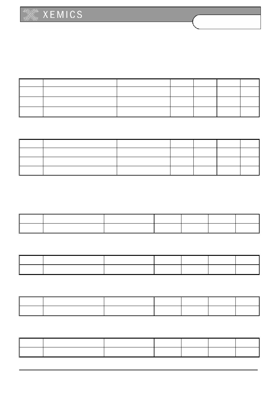
4.3.4 Timing Requirements of serial audio interface
Ref.
No. *
Characteristics
Test
Conditions
Min Typ Max
Unit
1
Master Clock Frequency for MCLK = 1/ T
1024
5.12
33
MHz
1
MCLK Duty Cycle
45 55
%
2
Rise Time for All Digital Signals
10
ns
3
Fall Time for All Digital Signals
10
ns
4
Hold time BCLK or FSYNC high after MCLK low
T/4
ns
5
Setup time BCLK or FSYNC high to MCLK low
T/4
ns
6
Hold time BCLK or FSYNC low after MCLK low
C
Load
= 10pF
T/4
ns
7
Setup time BCLK or FSYNC low to MCLK low
T/4
ns
8
Bit Clock Frequency for BCLK = 1 / T
BCLK
32xFSYNC
MCLK/2
MHz
9
Setup time data input SDI to BCLK low
T
BCLK
/4
ns
10
Hold time data input SDI after BCLK low
T
BCLK
/4
ns
11
Delay time SDO valid after BCLK high
not
applicable
ns
12
Setup time data input FSYNC to BCLK low
T
BCLK
/4
ns
13
Hold time data input FSYNC after BCLK low
T
BCLK
/4
ns
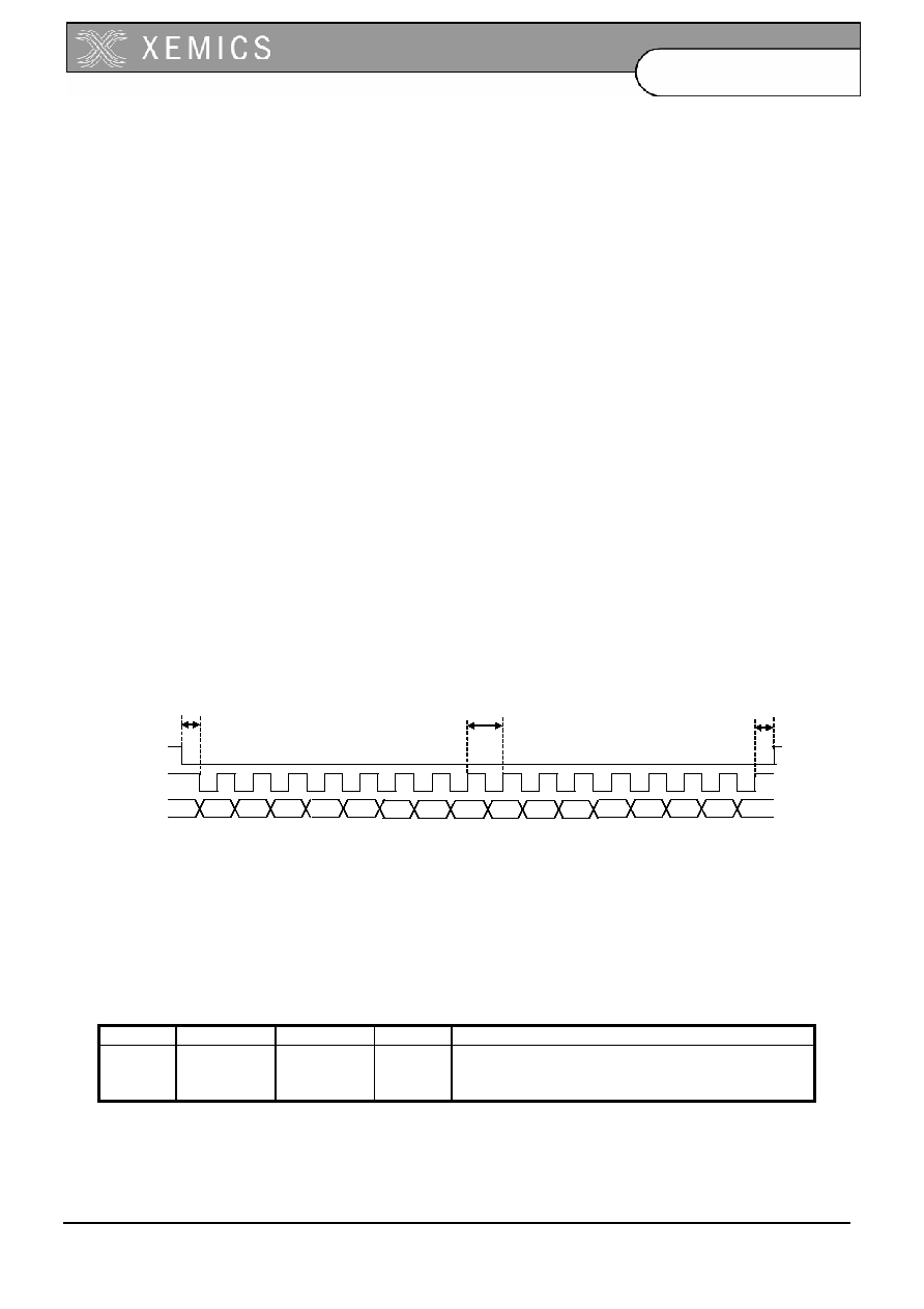
*see figure 13, 14 for LFS and 15, 16 for SFS
4.3.4.1 Timing diagram of the serial audio interface ≠ LFS mode
Figure 13: LFS mode, timing diagram
Figure 14: Timing diagram of the serial audio interface ≠ SFS mode
MCLK
BCLK
FSYNC
SDI
1
2
3
5
6
4
7
7
6
D15
D14
D13
D12
D11 D10
D9
D8
D7
D6
D5
D4
D3
D2
D1
D0
D15
D14
D13
D12
D11 D10
D9
D8
D7
D6
D5
D4
D3
D2
D1
D0
MCLK
BCLK
FSYNC
SDI
SDO
9
10
8
11
17
D0311-143
Data Sheet
XE3004
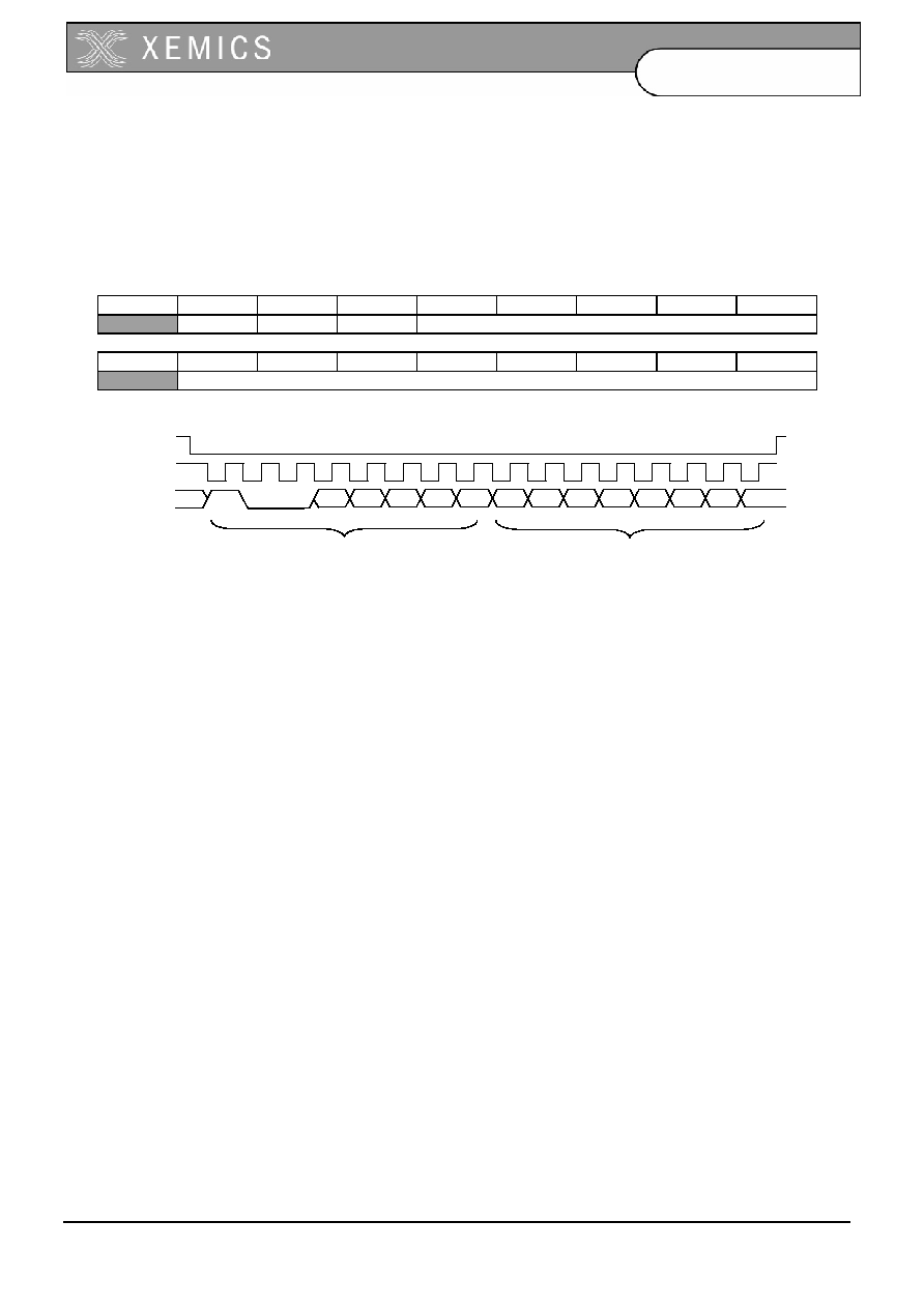
4.3.4.2 Timing diagram of the serial audio interface ≠ SFS mode
Figure 15: SFS mode, timing diagram
Figure 16: SFS mode, zoom timing diagram
MCLK
BCLK
FSYNC
SDI
1
2
3
4
7
5
6
D15
D14
D13
D12
D11 D10
D9
D8
D7
D6
D5
D4
D3
D2
D1
D0
D15
D14
D13
D12
D11 D10
D9
D8
D7
D6
D5
D4
D3
D2
D1
D0
MCLK
BCLK
FSYNC
SDI
SDO
9
10
8
11
12
13
18
D0311-143
Data Sheet
XE3004
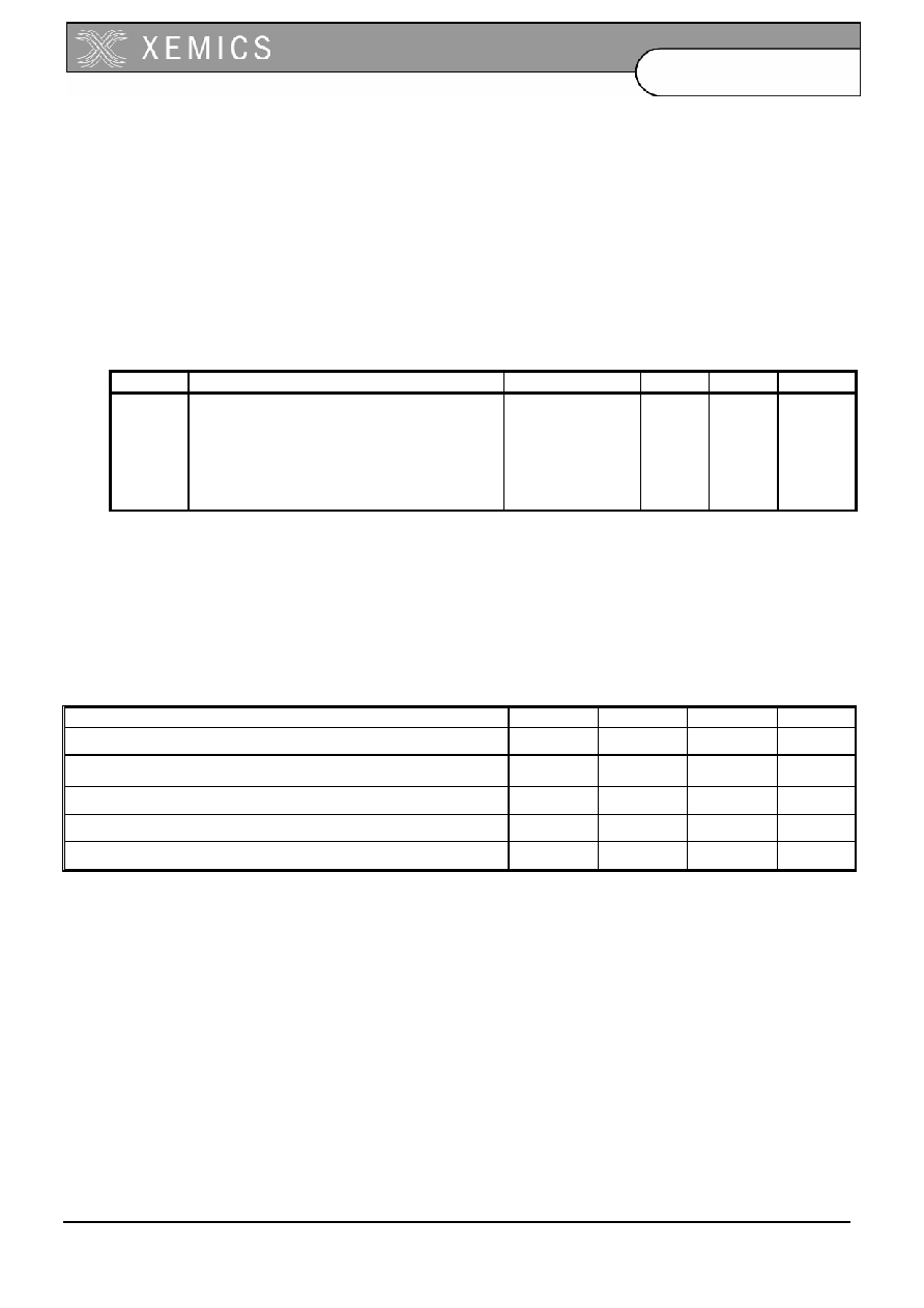
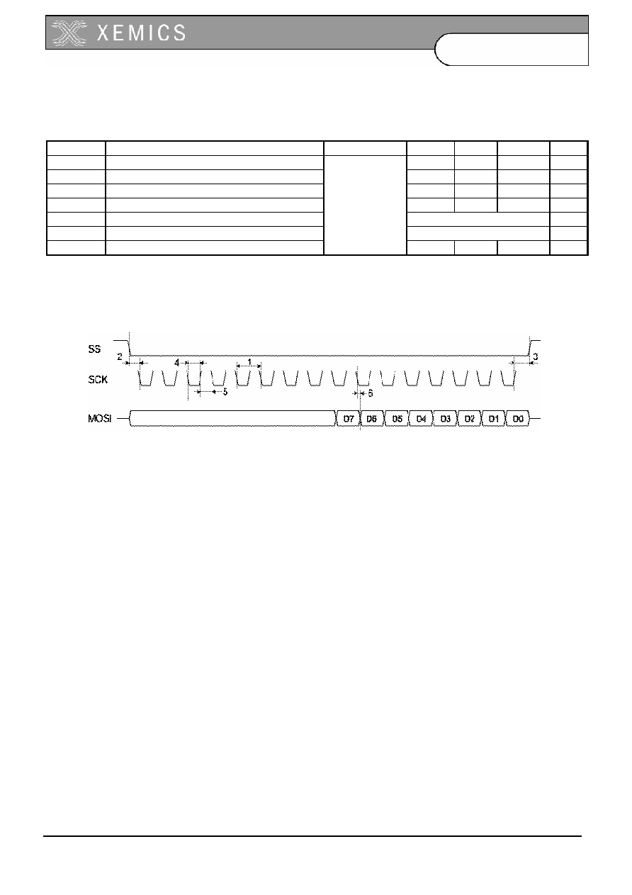
4.3.5 Timing Requirements of the Serial Peripheral Interface
Ref. No. *
Characteristics
Test Conditions
Min Typ Max Unit
1
Serial Clock Frequency for SCK = 1 / T
SCK
MCLK/2
MHz
1
MCLK Duty Cycle
45 55 %
2
Recovery Time
125 ns
3
Disable Time
C
Load
= 10pF
2T ns
4
Setup time MISO valid to SCK high
not applicable
ns
5
Hold time MISO valid after SCK high
not applicable
ns
6
Delay time MOSI valid after SCK low
T
SCK
/4
ns
* see figure 17
Figure 17: Serial Peripheral Interface timing
19
D0311-143
Data Sheet
XE3004
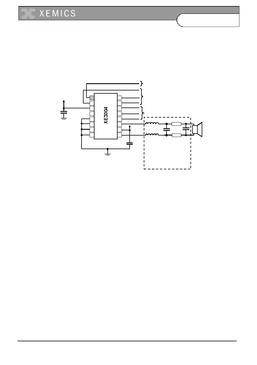
5 Application
Information
5.1 Application Schematics ≠ XE3004
GND
Vcc
Vcc
L=680µH
L
2µ2F
0.1µF
Master Clock
SPI
Serial Audio Interface
4µ7F
R
R
L
R=56
lowpass filter,
BluetoothTM voice application
MCLK = 2.048 MHz,
div_factor =1
1
5
6
7
8
MCLK
SS
NRESET
VSSA
VSSD
16
15
14
13
12
11
10
9
MOSI
VDD
SCK
SDI
BCLK
FSYNC
AOUTN
4
3
2
VSSA
VSSPA
AOUTP
VDDPA
0.1µF
Figure 18: Typical Application with 3
rd
order LC output Filter
The low pass filter between the DAC output and the speaker depends on the DAC settings and the speaker type.
20
D0311-143
Data Sheet
XE3004
6 Register
Description
6.1 Register Functional Summary
The following registers can be programmed by the SPI to configure the operation modes. See also chapter 3.2
Register Programming.
Name
Description
Function enable and clock division. The data in this register has the
following functions:
∑
Division of master clock
Register I
∑
Enable/disable DAC channel (DAC, power amplifier)
Audio Interface Configuration. The data in this register has the
following functions:
∑
Channel select receive
∑
Select master / slave mode
∑
Output
impedance
∑
Channel select transmit
∑
Select short / long frame sync
Register J
6.2 Register
Definitions
The complete register setup consists of 11 registers of 8 bits each, as shown in the table below. All registers are
preconfigured with the default values and do not have to be programmed by the user if no changes in the setup
are required.
The registers I and J can be used to configure the XE3004 differently than the default setup.
Register
Address
(hex)
Name
Default value (hex)
A 0x00
Reserved
0x48
B 0x01
Reserved
0x8F
C 0x02
Reserved
0xF0
D 0x03
Reserved
0x00
E 0x04
Reserved
0x0x
F 0x05
Reserved
0x82
G 0x06
Reserved
0x00
H 0x07
Reserved
0x00
I
0x08
Block on/off and clock division
0x00/0x01
J 0x09
Audio
interface
configuration 0x25/0x24
K 0x0A
Reserved
0x00
21
D0311-143
Data Sheet
XE3004
Register I (7:0)
address 0x08
block on/off and
clock division
Default value
0x00/0x01
Description
7:4
0000
reserved
3 EN_DAC 0
0:
enable
1: disable DA converter (DAC + PA)
2 0
reserved
1:0
MCLKDIV
00 or 01
Division factor of the master clock:
00: 1
01: 2
10: reserved
11: 4
The default is depending on the logic value of the pin SS
during startup (see Section 3.2)
SS=0, default will be set to 1
SS=1, default will be set to 0
Register J (7:0)
address 0x09
Audio
interface
configuration
Default
value
0x25/
0x24
Description
7
0
reserved
6 RX_FIRST_
SECOND
0
0: Receive audio data in the first 16-bit channel after the
frame synchronization.
1: Receive audio data in the second 16-bit channel after the
frame synchronization.
5 reserved
1
reserved
4
MASTER
0
1: enable audio interface in master mode (only for LFS)
0: enable audio interface in slave mode (LFS, LFS
Optimization or SFS)
3
0
reserved
2
1
reserved
1
0
reserved
0
PROTOCOL
0 or 1
1: Short Frame Synchronization mode (slave mode).
0: Long Frame Synchronization mode (master or slave
mode).
The default is depending on the logic value of the pin SCK during startup
(see Section 3.2)
SCK=0, default will be set to 1
SCK=1, default will be set to 0
22
D0311-143
Data Sheet
XE3004
7 Mechanical
Information
UNIT
A
1
A
2
A
3
b
p
c
D
(1)
E
(2)
(1)
e
H
E
L
L
p
Q
y
w
v
mm
0.15
0.05
0.95
0.80
0.30
0.19
0.2
0.1
5.1
4.9
4.5
4.3
0.65
6.6
6.2
0.4
0.3
0.40
0.06
8
0
o
o
0.13
0.1
0.2
1.0
DIMENSIONS (mm are the original dim
ensions)
0.75
0.50
w
M
b
p
D
Z
e
0.25
1
8
16
9
A
A
1
A
2
L
p
Q
detail X
L
(A )
3
H
E
E
c
v
M
A
X
A
y
A
max.
1.10
pin 1 index
Z
Figure 19: TSSOP16: Plastic Thin Shrink Small Outline Package, 16 leads, body width: 4.4 mm
©
XEMICS, 2003
All rights reserved. Reproduction in whole or in part is prohibited without the prior written consent of the copyright owner. The information
presented in this document does not form part of any quotation or contract, is believed to be accurate and reliable and may be changed
without notice. No liability will be accepted by the publisher for any consequence of its use. Publication thereof does not convey nor imply any
license under patent or other industrial or intellectual property rights.
XEMICS PRODUCTS ARE NOT DESIGNED, INTENDED, AUTHORIZED OR WARRANTED TO BE SUITABLE FOR USE IN LIFE-SUPPORT
APPLICATIONS, DEVICES OR SYSTEMS OR OTHER CRITICAL APPLICATIONS. INCLUSION OF XEMICS PRODUCTS IN SUCH
APPLICATIONS IS UNDERSTOOD TO BE UNDERTAKEN SOLELY AT THE CUSTOMER'S OWN RISK.
Should a customer purchase or use XEMICS products for any such unauthorized application, the customer shall indemnify and hold XEMICS
and its officers, employees, subsidiaries, affiliates, and distributors harmless against all claims, costs damages and attorney fees which could
arise.