Cool Solutions forWireless Connectivity
XEMICS SA * email: info@xemics.com * web: www.xemics.com
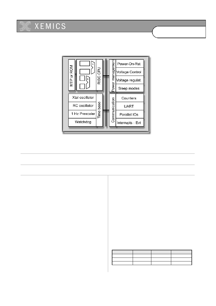
XE88LC03
Ultra Low-Power Microcontroller
General Description
∑
The XE88LC03 is an ultra low-power low-voltage
microcontroller unit (MCU) with extremely high effi-
ciency, allowing for 1 MIPS at 300uA at 2.4 V, and 8
x 8 bits multiplying in one clock cycle.
∑
XE88LC03 is available with on chip Multiple-Time-
Programmable (MTP) program memory.
Applications
∑
Internet connected appliances
∑
Portable, battery operated instruments
∑
RF system supervisor
∑
Remote control
∑
HVAC control
Key product Features
∑
Ultra low-power MCU
∑
300 uA at 1 MIPS operation
∑
6 uA at 32 kHz operation
∑
1 uA time keeping
∑
Low-voltage operation (2.4 - 5.5 V supply voltage)
∑
22 kB (8 kW) MTP, 512 + 8 B RAM
∑
4 counters
∑
PWM, UART
∑
Analog matrix switching
∑
independant RC and crystal oscillators
∑
5 reset, 17 interrupt, 8 event sources
∑
100 years MTP Flash retention at 55∞C
Ordering Information
Reference
Memory type Temperature
Package
XE88LC03MI000
MTP Flash
-40∞C to 85∞C
die
XE88LC03MI015
MTP Flash
-40∞C to 85∞C
SO28
XE88LC03MI026
MTP Flash
-40∞C to 85∞C
TQFP32
Datasheet XE88LC03
Data Acquisition Microcon
tr
oller
2
D0202-59
Datasheet XE88LC03
Data Acquisition Microcon
tr
oller
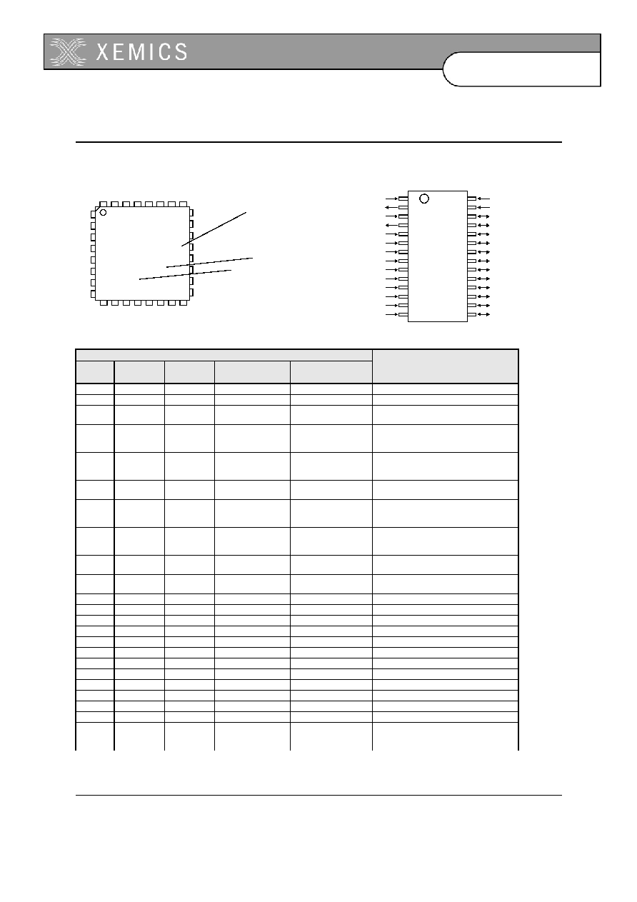
1 Detailed Pin Description
Pin
Description
Position
in SO28
Position in
TQFP32
Function
name
Second function
name
Type
1
13
Vbat
Power
Positive power supply
2
14
Vreg
Analog
Regulated supply
3
15
VPP
Vhigh/TEST
Special
Test mode/High voltage for MTP
programing
4
16
XOut
OscOut/ptck
Analog/Input
Connection to Xtal/
Peripheral clock for test and MTP
programing
5
17
XIn
OscIn/crck
Analog/Input
Connection to Xtal/
CoolRISC clock for test and MTP
programing
6
18
Vss
Power
Negative power supply, connected to
substrate
7
19
PA(0)
testin
Input
Input of Port A/
Data input for test and MTP programing/
Counter A input
8
20
PA(1)
testck
Input
Input of Port A/
Data clock for test and MTP programing/
Counter B input
9
21
PA(2)
Input
Input of Port A/
Counter C input/ Counter capture input
10
22
PA(3)
Input
Input of Port A/
Counter D input/ Counter capture input
11
23
PA(4)
Input
Input of Port A
12
24
PA(5)
Input
Input of Port A
13
25
PA(6)
Input
Input of Port A
14
26
PA(7)
Input
Input of Port A
15
27
PC(0)
Input/Output
Input-Output of Port C
16
28
PC(1)
Input/Output
Input-Output of Port C
17
29
PC(2)
Input/Output
Input-Output of Port C
18
30
PC(3)
Input/Output
Input-Output of Port C
31
PC(4)
Input/Output
Input-Output of Port C
32
PC(5)
Input/Output
Input-Output of Port C
1
PC(6)
Input/Output
Input-Output of Port C
2
PC(7)
Input/Output
Input-Output of Port C
19
3
PB(0)
testout
Input/Output/Analog
Input-Output-Analog of Port B/
Data output for test and MTP programing/
PWM output
Table 1.1:
Pin-out of the XE88LC03 in SO28 and TQFP32
(see Table "IO pins performances" on page 15 for drive capabilities of the pins)
1
2
3
4
5
6
28
27
26
25
24
23
22
21
20
19
18
17
16
15
XEM
I
C
S
X
E
8
8
L
C
0
3xI0
15
99
20
VBat
VReg
VPP
Xout
Xin
Vgnd
PA[0]
PA[1]
PA[2]
PA[3]
PA[4]
PA[5]
PA[6]
PA[7]
Res
RESET
PB[7]
PB[6]
PB[5]
PB[4]
PB[3]
PB[2]
PB[1]
PB[0]
PC[3]
PC[2]
PC[1]
PC[0]
Figure 1.1:
Pinout of the XE88LC03 in
SOP28 package
Figure 1.1:
Pinout of the XE88LC03 in
TQFP32 package
1
2
3
4
5
6
7
8
10
12
14
16
18
20
22
24
26
28
30
XEMICS
XE88LC03MI
N9K1444
9920
device type
production
packaging date
lot identification
3
D0202-59
Datasheet XE88LC03
Data Acquisition Microcon
tr
oller
20
4
PB(1)
Input/Output/Analog
Input-Output-Analog of Port B/
PWM output
21
5
PB(2)
Input/Output/Analog
Input-Output-Analog of Port B
22
6
PB(3)
SOU
Input/Output/Analog
Input-Output-Analog of Port B,
Output pin of USRT
23
7
PB(4)
S0/SCL
Input/Output/Analog
Input-Output-Analog of Port B/
Clock pin of USRT
24
8
PB(5)
S1/SIN
Input/Output/Analog
Input-Output-Analog of Port B/
Data input or input-output pin of USRT
25
9
PB(6)
Tx
Input/Output/Analog
Input-Output-Analog of Port B/
Emission pin of UART
26
10
PB(7)
Rx
Input/Output/Analog
Input-Output-Analog of Port B/
Reception pin of UART
27
11
RESET
Input
Reset pin (active high)
28
12
Reserved
Analog
To be connected to VSS
Pin
Description
Position
in SO28
Position in
TQFP32
Function
name
Second function
name
Type
Table 1.1:
Pin-out of the XE88LC03 in SO28 and TQFP32
(see Table "IO pins performances" on page 15 for drive capabilities of the pins)
4
D0202-59
Datasheet XE88LC03
Data Acquisition Microcon
tr
oller
2 Absolute maximum ratings
Stresses beyond these listed in this chapter may cause permanent damage to the device. No
functional operation is implied at or beyond these conditions. Exposure to these conditions for
an extended period may affect the device reliability.
Note:
1) For unprogrammed MTP devices. Blocking bits and software must be rewritten in MTP de-
vices if storage temperature exceedes storage temperature for programmed devices.
These devices are ESD sensitive. Although these devices feature proprietary ESD protection
structures, permanent damage may occur on devices subjected to high energy electrostatic
discharges. Proper ESD precautions have to be taken to avoid performance degradation or
loss of functionality.
Parameter
Value
Remarks
VBAT with respect to VSS
-0.3V to 6.0V
Input voltage on any input pin
VSS-0.3V to VBAT+0.3V
Storage temperature
-55
∞
C to 125
∞
C
1
Storage temperature for programmed MTP devices
-40
∞
C to 85
∞
C
1
Table 2.1:
Absolute maximum ratings
5
D0202-59
Datasheet XE88LC03
Data Acquisition Microcon
tr
oller
3 Electrical Characteristics
All specification are -40∞C to 85∞C unless otherwise noted. ROM operates up to 125∞C.
Note:
1) Power supply: 2.4 V - 5.5 V, temperature is 27∞C.
2) < 10 erase cycles.
3) More cycles possible during development, with restraint retention
4) With 2 MHz clock, all instructions are using exactly 1 clock cycle
5) Longer erase time may degrade retention
4 CPU
The XE88LC03 CPU is a low power RISC core. It has 16 internal registers for efficient imple-
mentation of the C compiler. Its instruction set is made of 35 generic instructions, all coded on
22 bits, with 8 addressing modes. All instructions are executed in one clock cycle, including
conditional jumps and 8x8 multiplication.
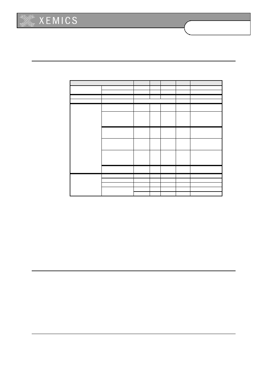
Operation conditions
min
typ
max
Unit
Remarks
Power supply
ROM version
2.4
5.5
V
MTP version
2.4
5.5
V
Operating speed
2.4 V to 5.5 V
0.032
2
MHz
Instruction cycle
any instruction
500
ns
4
Current requirement
CPU running
at 1 MIPS
310
uA
1
CPU running
at 32 kHz
on Xtal,
RC off
10
uA
1
CPU halt,
timer on Xtal,
RC off
1
uA
1
CPU halt,
timer on Xtal,
RC ready
1.7
uA
1
CPU halt,
Xtal off
timer on RC
at 100 kHz
1.4
uA
1
Voltage level
detection
15
uA
MTP Flash
instruction memory
Prog. voltage
11.5
V
Erase time
0.2
1
s
5
Write/Erase cycles
10
100
3
Data retention
10
years
85∞C, 2
100
years
55∞C, 2
Table 3.1:
Specifications and current requirement of the XE88LC03