Document Outline
- TABLE OF CONTENTS
- 1. General overview
- 2 XE88LC05/05A Performance
- 3. CPU
- 4 Memory mapping
- 5 System Block
- 6 Reset Block
- 7 Clock Generator
- 8 IRQ - Interrupt handler
- 9 Event handler
- 10 Low power RAM
- 11 Port A
- 12 Port B
- 13 Port C
- 14 UART
- 15 USRT
- 16. Acquisition chain
- 17. Vmult (Voltage Multiplier)
- 18. Signal D/A (DAS)
- 19. Bias D/A (DAB)
- 20. Counters/Timers/PWM
- 21 VLD (Voltage Level Detector)
- 22 Physical dimensions
Cool Solutions for Wireless Connectivity
XEMICS SA
∑
e-mail: info@xemics.com
∑
web: www.xemics.com
Datasheet XE88LC05/05A Sensing
Machine Data Acquisition MCU
with Zooming ADC and DACs
XE88LC05/05A
Sensing Machine
Data Acquisition with 16+10 bit ZoomingADCTM
and buffered 16 and 8 bit DACs
General Description
The XE88LC05A is a data acquisition ultra low-
power low-voltage system on a chip (SoC) with a
high efficiency microcontroller unit embedded
(MCU), allowing for 1 MIPS at 300uA and 2.4 V,
and multiplying in one clock cycle.
The XE88LC05A includes a high resolution
acquisition path with the 16+10 bits ZoomingADC
and two buffered DACs.
The XE88LC05A is available with on chip ROM or
Multiple-Time-Programmable (MTP) program
memory.
Applications
∑
Portable, battery operated instruments
∑
Current loop powered instruments
∑
Wheatstone bridge interfaces
∑
Pressure and chemical sensors
∑
HVAC
control
∑
Metering
∑
Sports watches, wrist instruments
Key product Features
∑
Low-power, high resolution ZoomingADC
∑
0.5 to 1000 gain with offset cancellation
∑
up to 16 bits analog to digital converter
∑
up to 13 inputs multiplexer
∑
Low-voltage
low-power
controller operation
∑
2 MIPS with 2.4 V to 5.5 V operation
∑
300 µA at 1 MIPS over voltage range
∑
22 kByte (8 kInstruction) MTP
∑
520 Byte RAM data memory
∑
RC and crystal oscillators
∑
5 reset, 22 interrupt, 8 event sources
∑
8 bit and 16 bit buffered DACs
∑
100 years MTP Flash retention at 55∞C
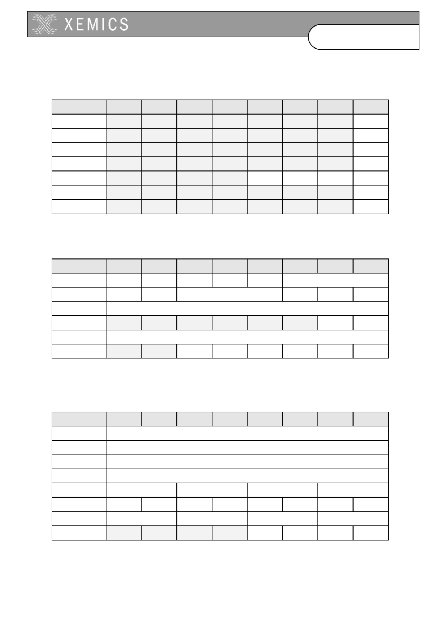
Ordering Information
Product Temperature
range
Memory
type
Package
XE88LC05MI028*
-40∞C to 85 ∞C
MTP
LQFP64
XE88LC05AMI000
-40∞C to 85 ∞C
MTP
die
XE88LC05AMI028
-40∞C to 85 ∞C
MTP
LQFP64
XE88LC05ARE000
-40∞C to 125 ∞C
ROM
die
XE88LC05ARE028
-40∞C to 125 ∞C
ROM
LQFP64
*Not for new designs

D0
304-40
Datasheet XE88LC05/05A Sensing
Machine Data Acquisition MCU
with Zooming ADC and DACs
TABLE OF CONTENTS
Chapter 1
XE88LC05/LC05A Overview
Chapter 2
XE88LC05/LC05A Performance
Chapter 3
XE88LC05/LC05A CPU
Chapter 4
XE88LC05/LC05A Memory
Chapter 5
System Block
Chapter 6
Reset generator
Chapter 7
Clock generation
Chapter 8
Interrupt handler
Chapter 9
Event handler
Chapter 10
Low power RAM
Chapter 11
Port A
Chapter 12
Port B
Chapter 13
Port C
Chapter 14
Universal Asynchronous Receiver/Transmitter (UART)
Chapter 15
Universal Synchronous Receiver/Transmitter (USRT)
Chapter 16
Acquisition Chain (ZoomingADCTM)
Chapter 17
Voltage multiplier
Chapter 18
Signal D/A (DAS)
Chapter 19
Bias D/A (DAB)
Chapter 20
Counters/Timers/PWM
Chapter 21
The Voltage Level Detector
Chapter 22
XE88LC05/LC05A Dimensions

1-1
LC05 - 1.2 ≠ 24 avril 2003
D0304-40
Datasheet
XE88LC05/05A
1. General overview
CONTENTS
1.1
Top schematic
1-2
1.1.1
General description
1-2
1.1.2
XE88LC05 vs XE88LC05A
1-4
1.2
Pin map
1-4
1.2.1
Bare die
1-4
1.2.2
LQFP-64
1-5
1.3
Pin assignment
1-6

1-2
D0304-40
Datasheet
XE88LC05/05A
1.1 Top schematic
1.1.1 General description
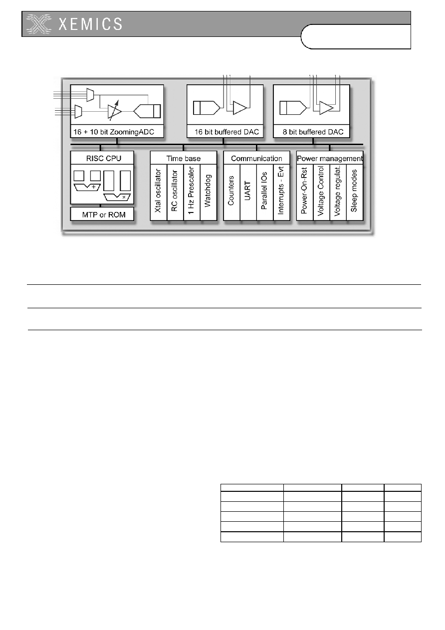
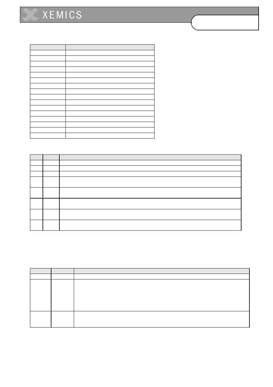
The top level block schematic of the circuit is shown in Figure 1-1. The heart of the circuit consists of
the Coolrisc816Æ CPU core. This core includes an 8x8 multiplier and 16 internal registers.
The bus controller generates all control signals for access to all data registers other than the CPU
internal registers.
The reset block generates the adequate reset signals for the rest of the circuit as a function of the set-
up contained in its control registers. Possible reset sources are the power-on-reset (POR), the
external pin RESET, the watchdog (WD), a bus error detected by the bus controller or a
programmable pattern on Port A. Different low power modes are implemented.
The clock generation and power management block sets up the clock signals and generates internal
supplies for different blocks. The clock can be generated from the RC oscillator (this is the start-up
condition), the crystal oscillator (XTAL) or an external clock source (given on the OSCIN pin).
The test controller generates all set-up signals for different test modes. In normal operation, it is used
as a set of 8 low power data registers. If power consumption is important for the application, the
variables that need to be accessed very often should be stored in these registers rather than in the
RAM.
The IRQ handler routes the interrupt signals of the different peripherals to the IRQ inputs of the CPU
core. It allows masking of the interrupt sources and it flags which interrupt source is active.
Events are generally used to restart the processor after a HALT period without jumping to a specified
address, i.e. the program execution resumes with the instruction following the HALT instruction. The
EVN handler routes the event signals of the different peripherals to the EVN inputs of the CPU core. It
allows masking of the interrupt sources and it flags which interrupt source is active.
The Port B is an 8 bit parallel IO port with analog capabilities. The URST, UART, and PWM block also
make use of this port.
The instruction memory is a 22-bit wide flash or ROM memory depending on the circuit version. Flash
and ROM versions have both 8k instruction memory. The data memory of this product is 512 byte
SRAM.
The Acquisition Chain is a high resolution acquisition path with the 16+10 bit fully differential
ZoomingADC
. The VMULT (voltage multiplier) powers a part of the Acquisition Chain.
The signal D/A (DAS) is a 16 bit D/A based on sigma-delta modulation. It includes a stand-alone
amplifier that can be used for analog output filtering.
The bias D/A (DAB) is an 8 bit low frequency D/A. It includes a stand-alone amplifier that is used to
drive large currents. It can be used to bias a sensor.
The Port A is an 8 bit parallel input port. It can also generate interrupts, events or a reset. It can be
used to input external clocks for the timer/counter/PWM block.
The Port C is a general purpose 8 bit parallel I/O port.
The USRT (universal synchronous receiver/transmitter) contains some simple hardware functions in
order to simplify the software implementation of a synchronous serial link.

1-3
D0304-40
Datasheet
XE88LC05/05A
INSTRUCTION MEMORY
B
U
S
C
O
N
T
R
O
L
L
E
R
TEST
CONTROLLER
RESET
BLOCK
WD
CLOCK
GENERATION/
POWER
MANAGEMENT
VREG
XTAL
RC
CPU
COOLRISC816
8
X
8
MULTIPLIER
16
CPU
REGISTERS
IRQ HANDLING
EVN HANDLING
PORT B
8 DATA REGISTERS
PORT A
PORT C
address
control
datain
dataout
reset
control
clocks
test
control
irq
evn
VPP/TEST
VBAT
VSS
RESET
OSCIN
OSCOUT
VREG
PB(7:0)
PA(7:0)
PC(7:0)
AC_R(3:0)
AC_A(7:0)
VMULT
DAS_OUT
DAS_AI_P
DAS_AI_M
DAS_AO
DAB_R_P
DAB_R_M
DAB_OUT
DAB_AI_P
DAB_AI_M
DAB_AO_P
DAB_AO_M
DATA
MEMORY
VLD
USRT
UART
COUNTERS
TIMERS
PWM
PB(
5
:4)
P
B
(7
:
6
)
PA
(3
:
0
)
PB(1:
0
)
POR
ACQUISITION
CHAIN
ZoomingADC
TM
VMULT
DAS
Signal D/A
DAB
Bias D/A
Figure 1-1. Block schematic of the XE88LC05/05A circuit.
The UART (universal asynchronous receiver/transmitter) contains a full hardware implementation of
the asynchronous serial link.
1-4
D0304-40
Datasheet
XE88LC05/05A
The counters/timers/PWM can take their clocks from internal or external sources (on Port A) and can
generate interrupts or events. The PWM is output on Port B.
The VLD (voltage level detector) detects the battery end of life with respect to a programmable
threshold.
1.1.2 XE88LC05 vs XE88LC05A
The XE88LC05A has a new RESET pin function. The action of the RESET pin of the XE88LC05A
resets the clock registers too and creates an additional short delay. See the RESET chapter for more
information.
1.2 Pin map
1.2.1 Bare die
(52.6,4123.5) PA(0)
(52.6, 3908.5) PA(1)
(52.6,3693.5) PA(2)
(52.6, 3478.5) PA(3)
(52.6, 3263.5) VBAT
(52.6, 3048.5) PA(4)
(52.6, 2833.5) PA(5)
(52.6, 2618.5) PA(6)
(52.6, 2403.5) PA(7)
(52.6, 2188.5) PC(0)
(52.6, 1973.5) PC(1)
(52.6, 1758.5) PC(2)
(52.6, 1543.5) PC(3)
(52.6, 1328.5) VSS
(52.6, 1113.5) PC(4)
(52.6, 898.5) PC(5)
(52.6, 683.5) PC(6)
(52.6, 468.5) PC(7)
AC_R(0) (3958.4, 4118.5)
AC_R(1) (3958.4, 3858.5)
VSS (3958.4, 3603.5)
AC_A(0) (3958.4, 3343.5)
AC_A(1) (3958.4, 3088.5)
AC_A(2) (3958.4, 2828.5)
AC_A(3) (3958.4, 2573.5)
AC_A(4) (3958.4, 2313.5)
VBAT (3958.4, 2058.5)
AC_A(5) (3958.4,1798.5)
AC_A(6) (3958.4, 1543.5)
AC_A(7) (3958.4, 1283.5)
AC_R(2) (3958.4, 1028.5)
AC_R(3) (3958.4, 768.5)
VPP/TEST (3958.4, 508.5)
VS
S
(
4
28.
5,
4
453
.4
)
OS
C
I
N
(
593
.
5
, 4
453
.
4
)
VS
S
(
7
58.
5,
4
453
.4
)
OS
C
OUT ( 923
.
5
, 4
453
.
4
)
R
E
SET
(
108
8
.
5,
44
53.4
)
V
M
U
LT
(
125
2
.
9,
44
53.4
)
VR
EG
(14
1
8
.5,
445
3.4
)
V
S
S
_
R
E
G
(15
88.
5,
4
453
.4
)
VS
S
(1
7
53.
5,
4
453
.4
)
VB
AT
(19
2
3
.5,
445
3.4
)
DAS_AO (3
114
.6, 445
3
.
4)
DAS_AI
_
M
(3
293
.5, 445
3
.
4)
DAS_
AI_P
(3
4
58.
5, 4
453.
4
)
DAS_OUT (3
6
28.5
,
4
4
5
3
.
4
)
(
3
9
8
.
5
,
4
7
.
6
)
P
B
(
0
)
(
5
3
3
.
5
,
4
7
.
6
)
P
B
(
1
)
(
6
6
8
.
5
,
4
7
.
6
)
P
B
(
2
)
(
7
9
8
.
5
,
4
7
.
6
)
P
B
(
3
)
(
9
3
3
.
5
,
4
7
.
6
)
P
B
(
4
)
(
1
0
63.
5,
47.
6)
V
B
A
T
(1
19
8
.
5
,
4
7
.
6
)
P
B
(
5
)
(1
32
8
.
5
,
4
7
.
6
)
P
B
(
6
)
(1
46
3
.
5
,
4
7
.
6
)
P
B
(
7
)
(
1
5
9
3
.
5,
47.
6)
D
A
B_R_
P
(17
2
8
.
5
,
47
.6)
DAB
_
R
_
M
(
1
8
58.
5,
47.
6)
D
A
B_O
U
T
(
2
0
42.
4,
47
.
6
)
D
A
B
_A
O
_
P
(
268
3.3,
4
7
.
6
)
D
A
B
_A
O
_
M
(
3
363
.5,
4
7
.
6
)
VSS
(34
9
8
.5,
47.
6)
DAB
_AI_P
(362
8.4,
47.
6
)
D
A
B
_A
I_M
4100
460
0
Figure 1-2. Die dimensions and pin coordinates (in µm)

1-5
D0304-40
Datasheet
XE88LC05/05A
1.2.2 LQFP-64
The XE88LC05/05A is delivered in a LQFP-64 package. The pin map is given below.
15
10
5
1
PC(7)
PC(6)
PC(5)
PC(4)
PC(3)
PC(2)
PC(1)
PC(0)
PA(7)
PA(6)
PA(5)
PA(4)
PA(3)
PA(2)
PA(1)
PA(0)
VPP/TEST
NC
AC_R(3)
AC_R(2)
AC_A(7)
AC_A(6)
AC_A(5)
AC_A(4)
AC_A(3)
AC_A(2)
AC_A(1)
AC_A(0)
AC_R(1)
AC_A(0)
NC
NC
NC
NC
DA
S_OUT
DA
S_
A
I
_
P
DA
S
_
AI_M
DA
S_
AO
VB
A
T
V
SS
V
SS_
REG
VR
EG
NC
VMULT
RE
SE
T
O
S
C
OUT
OS
C
I
N
NC
NC
DA
B_
A
I
_
M
DA
B_
A
I
_
P
DA
B_
A
O
_
M
DA
B_
A
O
_
P
DA
B_
O
U
T
DA
B_
R_
M
DA
B_
R_
P
P
B
(7
)
P
B
(6
)
P
B
(5
)
P
B
(4
)
P
B
(3
)
P
B
(2
)
P
B
(1
)
P
B
(0
)
35
40
45
30
25
20
50
55
60
Figure 1-3. LQFP-64 pin map
Package pin
name
Package pin
name
1 PA(0) 33
VPP/TEST
2 PA(1) 34 NC
3 PA(2) 35
AC_R(3)
4 PA(3) 36
AC_R(2)
5 PA(4) 37
AC_A(7)
6 PA(5) 38
AC_A(6)
7 PA(6) 39
AC_A(5)
8 PA(7) 40
AC_A(4)
9 PC(0) 41
AC_A(3)
10 PC(1) 42
AC_A(2)
11 PC(2) 43
AC_A(1)
12 PC(3) 44
AC_A(0)
13 PC(4) 45
AC_R(1)
14 PC(5) 46
AC_R(0)
15 PC(6) 47 NC
16 PC(7) 48 NC
17 PB(0) 49 NC
18 PB(1) 50 NC
19 PB(2) 51
DAS_OUT
20 PB(3) 52
DAS_AI_P

1-6
D0304-40
Datasheet
XE88LC05/05A
Package pin
name
Package pin
name
21 PB(4) 53
DAS_AI_M
22 PB(5) 54
DAS_AO
23 PB(6) 55 VBAT
24 PB(7) 56 VSS
25 DAB_R_P 57 VSS_REG
26 DAB_R_M 58 VREG
27 DAB_OUT 59
NC
28 DAB_AO_P 60 VMULT
29 DAB_AO_M 61 RESET
30 DAB_AI_P 62 OSCOUT
31 DAB_AI_M 63 OSCIN
32 NC 64 NC
Table 1-1. Bonding plan of the LQFP-64 package (LQFP 64L 10x10mm thick 1.6 mm)
1.3 Pin assignment
The table below gives a short description of the different pin assignments.
Pin
Assignment
VBAT
Positive power supply
VSS VSS_REG
Negative power supply
VREG
Connection for the mandatory external capacitor of the voltage regulator
VPP/TEST
High voltage supply for flash memory programming (NC in ROM versions)
RESET
Resets the circuit when the voltage is high
OSCIN/OSCOUT
Quartz crystal connections, also used for flash memory programming
PA(7:0)
Parallel input port A pins
PB(7:0)
Parallel I/O port B pins
PC(7:0)
Parallel I/O port C pins
AC_A(7:0)
Acquisition chain input pins
AC_R(3:0)
Acquisition chain reference pins
VMULT
Connection for the external capacitor if VBAT is below 3V
DAB_OUT
Bias D/A output
DAB_R_x
Bias D/A reference (x=P: plus, x=M: minus)
DAB_Ax_y
Bias D/A amplifier IO (x=I: input, x=O: output ; y=P: plus, y=M: minus)
DAS_OUT
Signal D/A output
DAS_AI_x
Signal D/A amplifier inputs (x=P: plus, x=M: minus)
DAS_AO
Signal D/A amplifier output
Table 1-2. Pin assignment
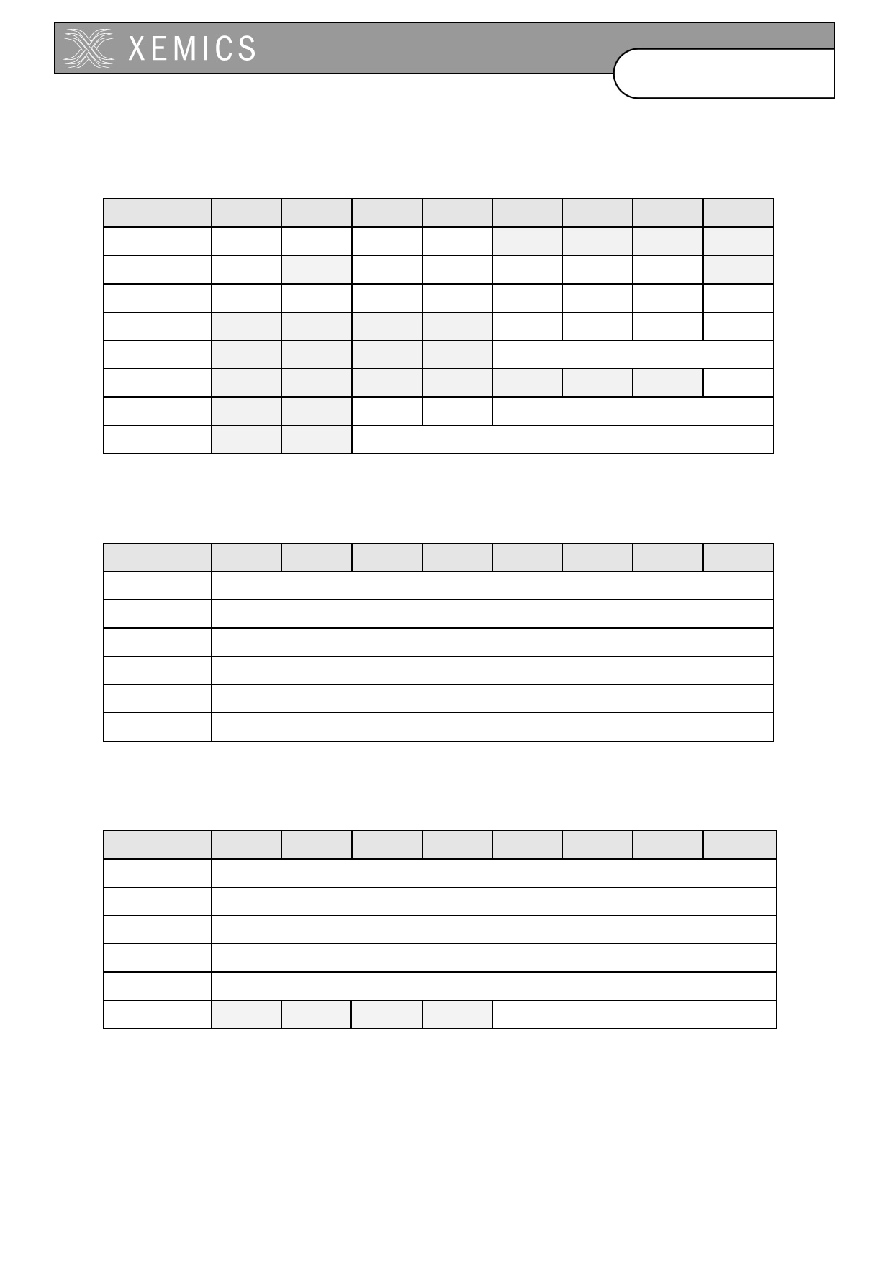
Table 1-3 gives a more detailed pin map for the different pins. It also indicates the possible I/O
configuration of these pins. The indications in blue bold are the configuration at start-up.
The pins CNTx pins are possible counter inputs, PWMx are possible PWM outputs.
1-7
D0304-40
Datasheet
XE88LC05/05A
pin function
I/O configuration
lqfp-64
first
second
third
AI
AO
DI
DO
OD
PU
POWER
1
PA(0)
CNTA
X
X
2
PA(1)
CNTB
X
X
3
PA(2)
CNTC
X
X
4
PA(3)
CNTD
X
X
5
PA(4)
X
X
6
PA(5)
X
X
7
PA(6)
X
X
8
PA(7)
X
X
9
PC(0)
X
X
10
PC(1)
X
X
11
PC(2)
X
X
12
PC(3)
X
X
13
PC(4)
X
X
14
PC(5)
X
X
15
PC(6)
X
X
16
PC(7)
X
X
17
PB(0)
PWM0 X
X
X
X X X
18
PB(1)
PWM1 X
X
X
X X X
19
PB(2)
X
X
X
X X X
20
PB(3)
X
X
X
X X X
21
PB(4)
USRT_S0
X
X
X
X X X
22
PB(5)
USRT_S1
X
X
X
X X X
23
PB(6)
UART_Tx
X
X
X
X X X
24
PB(7)
UART_Rx
X
X
X
X X X
25
DAB_R_P
X
26
DAB_R_M
X
27
DAB_OUT
X
28
DAB_AO_P
X
29
DAB_AO_M
X
30
DAB_AI_P
X
31
DAB_AI_M
X
33
VPP
TEST
X
35
AC_R(3)
X
36
AC_R(2)
X
37
AC_A(7)
X
38
AC_A(6)
X
39
AC_A(5)
X
40
AC_A(4)
X
41
AC_A(3)
X
42
AC_A(2)
X
43
AC_A(1)
X
44
AC_A(0)
X
45
AC_R(1)
X
46
AC_R(0)
X
51
DAS_OUT
X
52
DAS_AI_P
X
53
DAS_AI_M
X
54
DAS_AO
X
55
VBAT
X
1-8
D0304-40
Datasheet
XE88LC05/05A
pin function
I/O configuration
lqfp-64
first
second
third
AI
AO
DI
DO
OD
PU
POWER
56
VSS
X
57
VSS_REG
X
58
VREG
X
60
VMULT
X
61
RESET
X
62
OSCOUT
X
63
OSCIN
X
Pin map table legend:
blue bold: configuration at start up
AI: analog input
AO: analog output
DI: digital input
DO: digital output
OD: nMOS open drain output
PU: pull-up resistor
POWER: power supply
Table 1-3. Pin description table

2-1
LC05 - 1.0 ≠ 18 october 2002
D0304-40
Datasheet
XE88LC05/05A
2 XE88LC05/05A
Performance
2.1
Absolute maximum ratings
2-2
2.2 Operating
range
2-2
2.3 Supply
configurations
2-3
2.3.1 Flash circuit
2-3
2.3.2 ROM circuit
2-3
2.4 Current
consumption
2-5
2.5 Operating
speed
2-6
2.5.1 Flash version
2-6
2.5.2 ROM circuit version
2-6

2-2
D0304-40
Datasheet
XE88LC05/05A
2.1 Absolute maximum ratings
Table 2-1. Absolute maximum ratings
Min.
Max.
Note
Voltage applied to VBAT with respect to VSS
-0.3
6.0
V
Voltage applied to VPP with respect to VSS
VBAT-0.3
12
V
Voltage applied to all pins except VPP and VBAT
VSS-0.3
VBAT+0.3
V
Storage temperature (ROM device or unprogrammed
flash device)
-55 150
∞C
Storage temperature (programmed flash device)
-40
85
∞C
Stresses beyond the absolute maximal ratings may cause permanent damage to the device.
Functional operation at the absolute maximal ratings is not implied. Exposure to conditions beyond
the absolute maximal ratings may affect the reliability of the device.
2.2 Operating
range
Table 2-2. Operating range for the flash device
Min.
Max.
Note
Voltage applied to VBAT with respect to VSS
2.4
5.5
V
Voltage applied to VBAT with respect to VSS during
the flash programming
3.3 5.5
V
1
Voltage applied to VPP with respect to VSS
VBAT
11.5
V
Voltage applied to all pins except VPP and VBAT
VSS
VBAT
V
Operating temperature range
-40
85
∞C
Capacitor on VREG (flash version)
0.8
1.2
µ
F
2
Capacitor on VMULT
1.0
3.0
nF
3
1. During the programming of the device, the supply voltage should at least be equal to the
supply voltage used during normal operation.
2. The capacitor on VREG is mandatory.
3. The capacitor on VMULT is optional. The capacitor has to be present if the multiplier is
enabled. The multiplier has to be enabled if VBAT<3.0V.
Table 2-3. Operating range for the ROM device
Min.
Max.
Note
Voltage applied to VBAT with respect to VSS
2.4
5.5
V
Voltage applied to all pins except VPP and VBAT
VSS
VBAT
V
Operating temperature range
-40
125
∞C
Capacitor on VREG
0.1
1.2
µ
F
1
Capacitor on VMULT
1.0
3.0
nF
2
1. The capacitor may be omitted when VREG is connected to VBAT.
2. The capacitor on VMULT is optional. The capacitor has to be present if the multiplier is
enabled. The multiplier has to be enabled if VBAT<3.0V.
All specifications in this document are valid for the complete operating range unless otherwise
specified.
2-3
D0304-40
Datasheet
XE88LC05/05A
Table 2-4. Operating range of the Flash memory
Min.
Max.
Note
Retention time at 85∞C
10
years 1
Retention time at 55∞C
100
years 1
Number of programming cycles
10
2
1. Valid only if programmed using a programming tool that is qualified
2. Circuits can be programmed more than 10 times but after that, the retention time is no
longer guaranteed. All qualification tests have been done after 10 cycles.
2.3 Supply
configurations
2.3.1 Flash
circuit
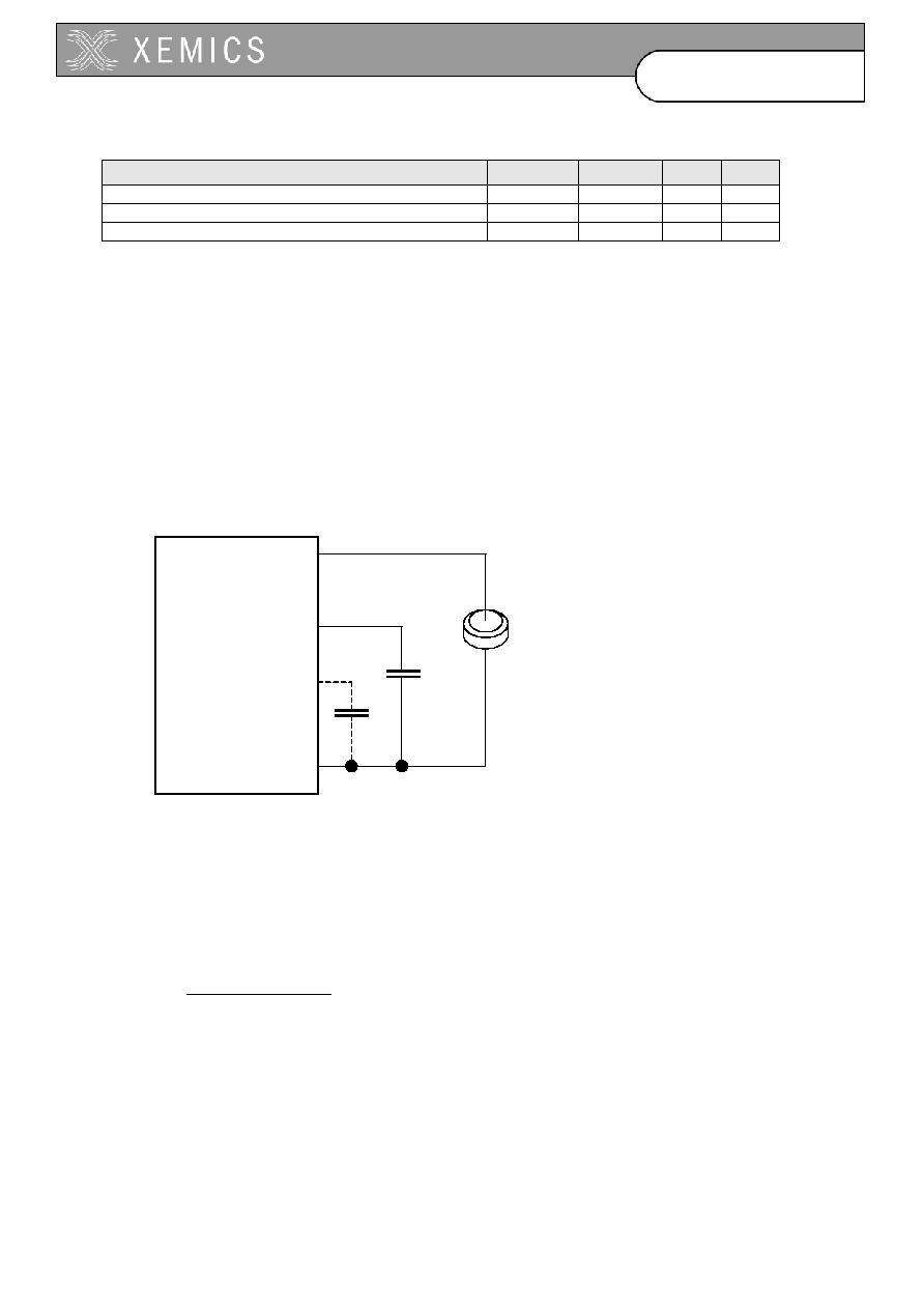
The flash version of the circuit can be run from a supply between 2.4V and 5.5V (Figure 2-1). The
capacitor on VREG has to be connected at all times (value in Table 2-2) to guarantee proper
operation of the device. The capacitor on VMULT is only required if the circuit is to be operated below
3V.
VBAT
VREG
VMULT
VSS
2.4V ≠ 5.5V
C
vreg
C
vmult
Figure 2-1. Supply configuration for the flash circuit.
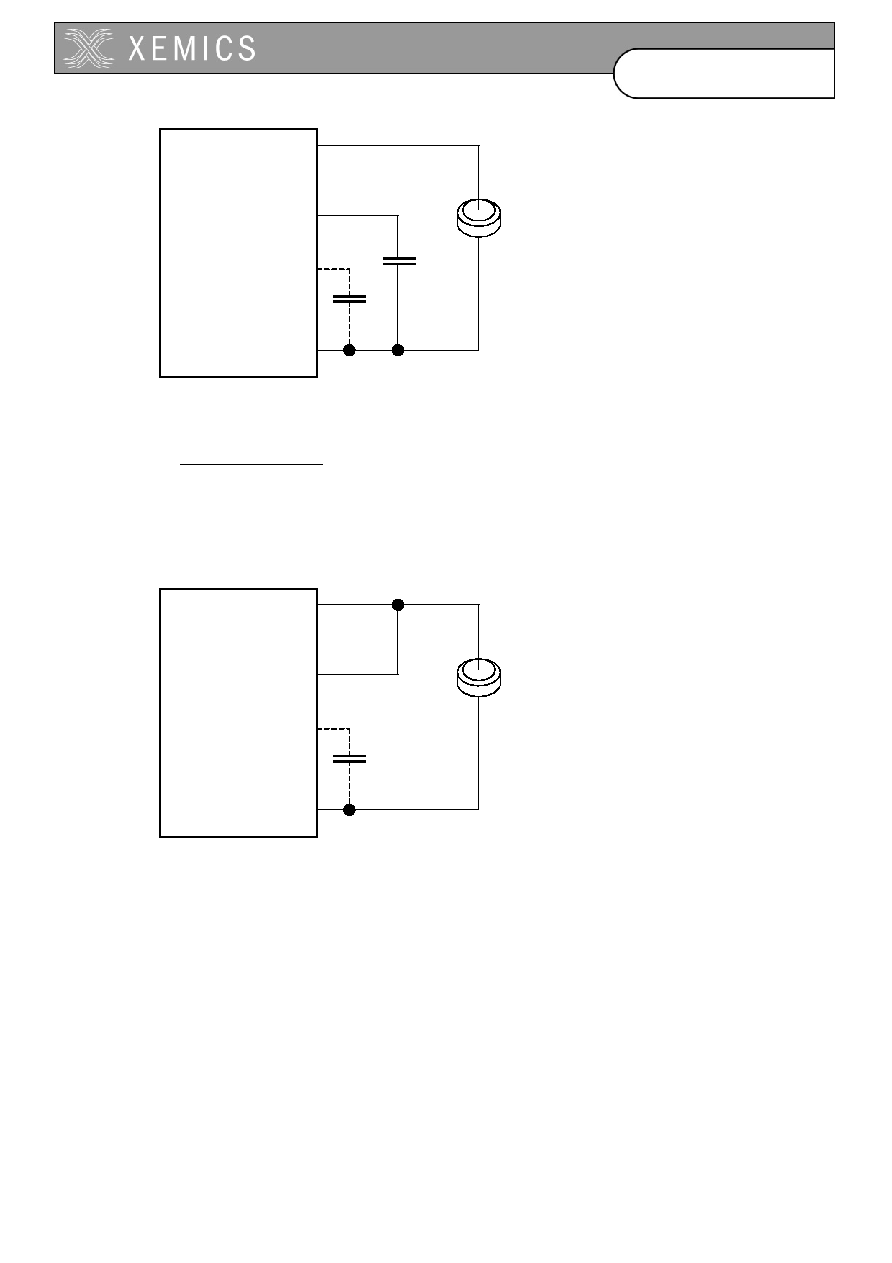
2.3.2 ROM
circuit
For the ROM version, two possible operating modes exist: with and without voltage regulator. Using
the voltage regulator, low power consumption will be obtained even with supply voltages above 2.4V.
Without the voltage regulator (i.e. VREG short-circuited to VBAT), a higher speed can be obtained.
2.3.2.1
Low power operation
In this case, the internal voltage regulator is used in order to maintain low power consumption
independent from the supply voltage. The capacitor on VREG has to be connected at all times (value
in Table 2-3) to guarantee proper operation of the device. The capacitor on VMULT has to be
connected only when VBAT<3V.
2-4
D0304-40
Datasheet
XE88LC05/05A
VBAT
VREG
VMULT
VSS
2.4V ≠ 5.5V
C
vreg
C
vmult
Figure 2-2. Supply voltage connections for low power operation of the ROM version.
2.3.2.2
High speed operation
In this case, the internal voltage regulator is not used. The operation speed of the circuit can be
increased with increasing supply voltage but the supply current will also increase. The capacitor on
VMULT has to be connected only when VBAT<3V. In this case, the supply voltage can decrease
down to 2.15V. Beware however that the zoomingADC
TM
will not run below 2.4V (see Figure 2-4). In
this configuration, the circuit can not be used above 3.3V.
VBAT
VREG
VMULT
VSS
2.15V ≠ 3.3V
C
vmult
Figure 2-3. Supply voltage connections for high speed operation of the ROM version.
2-5
D0304-40
Datasheet
XE88LC05/05A
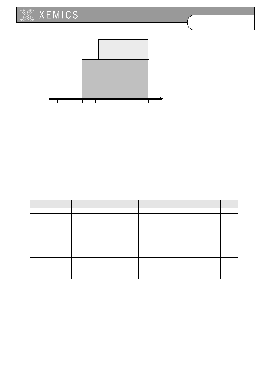
0 2.15 2.4 3.3 VBAT (V)
CPU
parallel and serial ports
RC and crystal oscillator
VLD
Counters and PWM
DAS (without amplifier)
acquisition chain
voltage multiplier
DAB
Figure 2-4. Operation range of the different circuit blocks
2.4 Current
consumption
The tables below give the current consumption for the circuit in different configurations. The figures
are indicative only and may change as a function of the actual software implemented in the circuit.
Table 2-5 gives the current consumption for the flash version of the circuit. The peripherals are
disabled. The parallel ports A and B are configured in input with pull up, the parallel port C is
configured as an output. Their pins are not connected externally. The pin RESET is connected to VSS
and the pin VPP/TEST is connected to VBAT. The inputs of the acquisition chain are connected to
VSS.
Table 2-5. Typical current consumption of the XE88LC05 version (8k instructions flash memory)
Operation mode
CPU
RC
Xtal
Consumption comments
Note
High speed CPU
1 MIPS
1 MHz
Off
310
µ
A 2.4V<>5.5V,
27
∞
C
Low power CPU
32 kIPS
Off
32 kHz
10
µ
A
2.4V <>5.5V, 27
∞
C
Low power time
keeping
HALT Off 32
kHz 1.0
µ
A
2.4V <>5.5V, 27
∞
C
Fast wake-up
time keeping
HALT Ready 32kHz
1.7
µ
A
2.4V <>5.5V, 27
∞
C
Immediate wake-
up time keeping
HALT 100
kHz Off
1.4
µ
A
2.4V <>5.5V, 27
∞
C
VLD static current
15
µ
A
2.4V <>5.5V, 27
∞
C
16 bit resolution
data acquisition
HALT 2
MHz Off
190
µ
A 3.0V,
27
∞
C
1
12 bit , gain 100,
data acquisition
HALT 2
MHz Off
460
µ
A 3.0V,
27
∞
C
2
1. PGA disabled, ADC enabled, 16 bit resolution
2. PGA 1 disabled, PGA 2 and 3 enabled, ADC enabled, 12 bit resolution
For more information concerning the current consumption of the zoomingADC
TM
, see the chapter
power consumption in the acquisition chain documentation which shows the current consumption of
this block as a function of temperature and voltage and for different configurations of the PGA and
ADC.
The power consumption of the ROM version of the circuit is identical if it is configured as shown in
Figure 2-2. In the high speed configuration, the current consumption will increase proportional with
VBAT.

2-6
D0304-40
Datasheet
XE88LC05/05A
2.5 Operating
speed
2.5.1 Flash
version
The speed of the devices is not highly dependent upon the supply voltage. However, by limiting the
temperature range, the speed can be increased. The minimal guaranteed speed as a function of the
supply voltage and maximal temperature operating temperature is given in Figure 2-5.
0
1
2
3
4
2
2.5
3
3.5
4
4.5
5
5.5
supply voltage VBAT (V)
sp
eed
(MIPS)
85∞C
45∞C
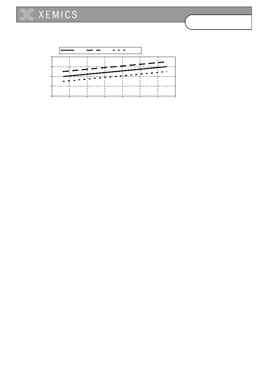
Figure 2-5. Guaranteed speed as a function of the supply voltage and maximal temperature.
2.5.2
ROM circuit version
2.5.2.1
Low power supply configuration
In the low power supply configuration as shown in Figure 2-2, the operating speed does not depend
highly on the supply voltage as shown in Figure 2-6.
0
0.5
1
1.5
2
2.5
3
3.5
2
2.5
3
3.5
4
4.5
5
5.5
supply voltage VBAT (V)
speed (MIPS)
85∞C
45∞C
125∞C
Figure 2-6. Guaranteed speed as a function of supply voltage and for different maximal temperatures
using the voltage regulator.
2.5.2.2
High speed supply configuration
In the high speed supply configuration of Figure 2-3, the guaranteed speed of the circuit is shown in
Figure 2-7.
2-7
D0304-40
Datasheet
XE88LC05/05A
0
1
2
3
4
2
2.2
2.4
2.6
2.8
3
3.2
3.4
supply voltage VBAT (V)
speed (MIPS)
85∞C
45∞C
125∞C
Figure 2-7. Guaranteed speed as a function of supply voltage and for three temperature ranges when
VREG=VBAT.

3-1
D0304-40
Datasheet
XE88LC05/05A
3. CPU
CONTENTS
3.1 CPU
description
3-2
3.2
CPU internal registers
3-2
3.3
CPU instruction short reference
3-4

3-2
D0304-40
Datasheet
XE88LC05/05A
3.1 CPU
description
The CPU of the XE8000 series is a low power RISC core. It has 16 internal registers for efficient
implementation of the C compiler. Its instruction set is made up of 35 generic instructions, all coded
on 22 bits, with 8 addressing modes. All instructions are executed in one clock cycle, including
conditional jumps and 8x8 multiplication. The circuit therefore runs on 1 MIPS on a 1MHz clock.
The CPU hardware and software description is given in the document "Coolrisc816 Hardware and
Software Reference Manual". A short summary is given in the following paragraphs.
The good code efficiency of the CPU core makes it possible to compute a polynomial like
Y
B
B
X
Y
A
A
Z
+
+
+
=
1
0
1
0
)
(
in less than 300 clock cycles (software code generated by the
XEMICS C-compiler, all numbers are signed integers on 16 bits).
3.2
CPU internal registers
As shown in Figure 3-1, the CPU has 16 internal 8-bit registers. Some of these registers can be
concatenated to a 16-bit word for use in some instructions. The function of these registers is defined
in Table 3-1. The status register stat (Table 3-2) is used to manage the different interrupt and event
levels. An interrupt or an event can both be used to wake up after a HALT instruction. The difference
is that an interrupt jumps to a special interrupt function whereas an event continues the software
execution with the instruction following the HALT instruction.
The program counter (PC) is a 16 bit register that indicates the address of the instruction that has to
be executed. The stack (ST
n
) is used to memorise the return address when executing subroutines or
interrupt routines.
Instruction
memory
22bit
CPU
CP
U inter
n
al
r
e
g
i
ster
s
a
stat
iph
ipl
i3h
i3l
i2h
i2l
i1h
i1l
i0h
i0l
r3
r2
r1
r0
Data memory
da
t
a
b
u
s
inst
ru
cti
o
n bu
s
PC
ST
1
ST
2
ST
3
ST
4
program counter stack
Figure 3-1. CPU internal registers
3-3
D0304-40
Datasheet
XE88LC05/05A
Register name Register function
r0 general
purpose
r1 general
purpose
r2 general
purpose
r3
data memory offset
i0h
MSB of the data memory index i0
i0l
LBS of the data memory index i0
i1h
MSB of the data memory index i1
i1l
LBS of the data memory index i1
i2h
MSB of the data memory index i2
i2l
LBS of the data memory index i2
i3h
MSB of the data memory index i3
i3l
LBS of the data memory index i3
iph
MSB of the program memory index ip
ipl
LBS of the program memory index ip
stat status
register
a accumulator
Table 3-1. CPU internal register definition
bit
name function
7
IE2
enables (when 1) the interrupt request of level 2
6
IE1
enables (when 1) the interrupt request of level 1
5
GIE
enables (when 1) all interrupt request levels
4
IN2
interrupt request of level 2. The interrupts labelled "low" in the interrupt handler are
routed to this interrupt level. This bit has to be cleared when the interrupt is served.
3
IN1
interrupt request of level 1. The interrupts labelled "mid" in the interrupt handler are
routed to this interrupt level. This bit has to be cleared when the interrupt is served.
2
IN0
interrupt request of level 0. The interrupts labelled "hig" in the interrupt handler are
routed to this interrupt level. This bit has to be cleared when the interrupt is served.
1
EV1
event request of level 1. The events labelled "low" in the event handler are routed to
this event level. This bit has to be cleared when the event is served.
0
EV0
event request of level 1. The events labelled "hig" in the event handler are routed to
this event level. This bit has to be cleared when the event is served.
Table 3-2. Status register description
The CPU also has a number of flags that can be used for conditional jumps. These flags are defined
in Table 3-3.
symbol name
function
Z
zero
Z=1 when the accumulator a content is zero
C
carry
This flag is used in shift or arithmetic operations.
For a shift operation, it has the value of the bit that was shifted out (LSB for shift
right, MSB for shift left).
For an arithmetic operation with unsigned numbers:
it is 1 at occurrence of an overflow during an addition (or equivalent).
it is 0 at occurrence of an underflow during a subtraction (or equivalent).
V
overflow This flag is used in shift or arithmetic operations.
For arithmetic or shift operations with signed numbers, it is 1 if an overflow or
underflow occurs.
Table 3-3. Flag description

3-4
D0304-40
Datasheet
XE88LC05/05A
3.3
CPU instruction short reference
Table 3-4 shows a short description of the different instructions available on the Coolrisc816. The
notation
cc
in the conditional jump instruction refers to the condition description as given in Table 3-6.
The notation
reg, reg1, reg2, reg3
refers to one of the CPU internal registers of Table 3-1. The
notation
eaddr
and
DM(eaddr)
refer to one of the extended address modes as defined in Table 3-5.
The notation DM(xxx) refers to the data memory location with address xxx.
Instruction
Modification Operation
Jump addr[15:0]
-,-,-, -
PC := addr[15:0]
Jump ip
-,-,-, -
PC := ip
J
cc
addr[15:0]
-,-,-, -
if
cc
is true then PC := addr[15:0]
J
cc
ip
-,-,-, -
if
cc
is true then PC := ip
Call addr[15:0]
-,-,-, -
ST
n+1
:= ST
n
(n>1); ST
1
:= PC+1; PC := addr[15:0]
Call ip
-,-,-, -
ST
n+1
:= ST
n
(n>1); ST
1
:= PC+1; PC := ip
Calls addr[15:0]
-,-,-, -
ip := PC+1; PC := addr[15:0]
Calls ip
-,-,-, -
ip := PC+1; PC := ip
Ret
-,-,-, -
PC := ST
1
; ST
n
:= ST
n+1
(n>1)
Rets
-,-,-, -
PC := ip
Reti
-,-,-, -
PC := ST
1
; ST
n
:= ST
n+1
(n>1); GIE :=1
Push
-,-,-, -
PC := PC+1; ST
n+1
:= ST
n
(n>1); ST
1
:= ip
Pop
-,-,-, -
PC := PC+1; ip := ST
1
; ST
n
:= ST
n+1
(n>1)
Move
reg
,#data[7:0]
-,-, Z, a
a := data[7:0];
reg
:= data[7:0]
Move
reg1
,
reg2
-,-, Z, a
a :=
reg2
;
reg1
:=
reg2
Move
reg
,
eaddr
-,-, Z, a
a :=
DM(eaddr)
;
reg
:=
DM(eaddr)
Move
eaddr
,
reg
-,-,-, -
DM(eaddr)
:=
reg
Move addr[7:0],#data[7:0]
-,-,-, -
DM(addr[7:0]) := data[7:0]
Cmvd
reg1
,
reg2
-,-, Z, a
a :=
reg2
; if C=0 then
reg1
:= a;
Cmvd
reg
,
eaddr
-,-, Z, a
a :=
DM(eaddr)
;
if C=0 then
reg
:= a
Cmvs
reg1
,
reg2
-,-, Z, a
a :=
reg2
; if C=1 then
reg1
:= a;
Cmvs
reg
,
eaddr
-,-, Z, a
a :=
DM(eaddr)
;
if C=1 then
reg
:= a
Shl
reg1
,
reg2
C, V, Z, a
a :=
reg2
<<1;
a[0] := 0; C :=
reg2[7]
;
reg1
:= a
Shl
reg
C, V, Z, a
a :=
reg
<<1; a[0] := 0; C :=
reg[7]
;
reg
:= a
Shl
reg
,
eaddr
C, V, Z, a
a :=
DM(eaddr)
<<1; a[0] :=0; C :=
DM(eaddr)[7]
;
reg
:= a
Shlc
reg1
,
reg2
C, V, Z, a
a :=
reg2
<<1;
a[0] := C; C :=
reg2[7]
;
reg1
:= a
Shlc
reg
C, V, Z, a
a :=
reg
<<1; a[0] := C; C :=
reg[7]
;
reg
:= a
Shlc
reg
,
eaddr
C, V, Z, a
a :=
DM(eaddr)
<<1; a[0] := C; C :=
DM(eaddr)[7]
;
reg
:= a
Shr
reg1
,
reg2
C, V, Z, a
a :=
reg2
>>1;
a[7] := 0; C :=
reg2[0]
;
reg1
:=a
Shr
reg
C, V, Z, a
a :=
reg
>>1; a[7] := 0; C :=
reg[0]
;
reg
:= a
Shr
reg
,
eaddr
C, V, Z, a
a :=
DM(eaddr)
>>1; a[7] := 0; C :=
DM(eaddr)[0]
;
reg
:= a
Shrc
reg1
,
reg2
C, V, Z, a
a :=
reg2
>>1;
a[7] := C; C :=
reg2[0]
;
reg1
:= a
Shrc
reg
C, V, Z, a
a :=
reg
>>1; a[7] := C; C :=
reg[0]
;
reg
:= a
Shrc
reg
,
eaddr
C, V, Z, a
a :=
DM(eaddr)
>>1; a[7] := C; C :=
DM(eaddr)[0]
;
reg
:= a
Shra
reg1
,
reg2
C, V, Z, a
a :=
reg2
>>1;
a[7] :=
reg2[7]
; C :=
reg2[0]
;
reg1
:= a
Shra
reg
C, V, Z, a
a :=
reg
>>1; a[7] :=
reg[7]
; C :=
reg[0]
;
reg
:= a
Shra
reg
,
eaddr
C, V, Z, a
a :=
DM(eaddr)
>>1; a[7] :=
DM(eaddr)[7]
; C :=
DM(eaddr)[0]
;
reg
:= a
Cpl1
reg1
,
reg2
-,-, Z, a
a := NOT(
reg2
);
reg1
:= a
Cpl1
reg
-,-, Z, a
a := NOT(
reg
);
reg
:= a
Cpl1
reg
,
eaddr
-,-, Z, a
a := NOT(
DM(eaddr)
);
reg
:= a
Cpl2
reg1
,
reg2
C, V, Z, a
a := NOT(
reg2
)+1; if a=0 then C:=1 else C := 0;
reg1
:= a
Cpl2
reg
C, V, Z, a
a := NOT(
reg
)+1; if a=0 then C:=1 else C := 0;
reg
:= a
Cpl2
reg
,
eaddr
C, V, Z, a
a := NOT(
DM(eaddr)
)+1; if a=0 then C:=1 else C := 0;
reg
:= a
Cpl2c
reg1
,
reg2
C, V, Z, a
a := NOT(
reg2
)+C; if a=0 and C=1 then C:=1 else C := 0;
reg1
:= a
Cpl2c
reg
C, V, Z, a
a := NOT(
reg
)+C; if a=0 and C=1 then C:=1 else C := 0;
reg
:= a
Cpl2c
reg
,
eaddr
C, V, Z, a
a := NOT(
DM(eaddr)
)+C; if a=0 and C=1 then C:=1 else C := 0;
reg
:= a
Inc
reg1
,
reg2
C, V, Z, a
a :=
reg2
+1; if a=0 then C := 1 else C := 0;
reg1
:= a
Inc
reg
C, V, Z, a
a :=
reg
+1; if a=0 then C := 1 else C := 0;
reg
:= a
Inc
reg
,
eaddr
C, V, Z, a
a :=
DM(eaadr)
+1; if a=0 then C := 1 else C := 0;
reg
:= a
Incc
reg1
,
reg2
C, V, Z, a
a :=
reg2
+C; if a=0 and C=1 then C := 1 else C := 0;
reg1
:= a
Incc
reg
C, V, Z, a
a :=
reg
+C; if a=0 and C=1 then C := 1 else C := 0;
reg
:= a
Incc
reg
,
eaddr
C, V, Z, a
a :=
DM(eaadr)
+C; if a=0 and C=1 then C := 1 else C := 0;
reg
:= a
Dec
reg1
,
reg2
C, V, Z, a
a :=
reg2
-1; if a=hFF then C := 0 else C := 1;
reg1
:= a

3-5
D0304-40
Datasheet
XE88LC05/05A
Dec
reg
C, V, Z, a
a :=
reg
-1; if a=hFF then C := 0 else C := 1;
reg
:= a
Dec
reg
,
eaddr
C, V, Z, a
a :=
DM(eaddr)
-1; if a=hFF then C := 0 else C := 1;
reg
:= a
Decc
reg1
,
reg2
C, V, Z, a
a :=
reg2
-(1-C); if a=hFF and C=0 then C := 0 else C := 1;
reg1
:= a
Decc
reg
C, V, Z, a
a :=
reg
-(1-C); if a=hFF and C=0 then C := 0 else C := 1;
reg
:= a
Decc
reg
,
eaddr
C, V, Z, a
a :=
DM(eaddr)
-(1-C); if a=hFF and C=0 then C := 0 else C := 1;
reg
:= a
And
reg
,#data[7:0]
-,-, Z, a
a :=
reg
and data[7:0];
reg
:= a
And
reg1
,
reg2
,
reg3
-,-, Z, a
a :=
reg2
and
reg3
;
reg1
:= a
And
reg1
,
reg2
-,-, Z, a
a :=
reg1
and
reg2
;
reg1
:= a
And
reg
,
eaddr
-,-, Z, a
a :=
reg
and
DM(eaddr)
;
reg
:= a
Or
reg
,#data[7:0]
-,-, Z, a
a :=
reg
or data[7:0];
reg
:= a
Or
reg1
,
reg2
,
reg3
-,-, Z, a
a :=
reg2
or
reg3
;
reg1
:= a
Or
reg1
,
reg2
-,-, Z, a
a :=
reg1
or
reg2
;
reg1
:= a
Or
reg
,
eaddr
-,-, Z, a
a :=
reg
or
DM(eaddr)
;
reg
:= a
Xor
reg
,#data[7:0]
-,-, Z, a
a :=
reg
xor data[7:0];
reg
:= a
Xor
reg1
,
reg2
,
reg3
-,-, Z, a
a :=
reg2
xor
reg3
;
reg1
:= a
Xor
reg1
,
reg2
-,-, Z, a
a :=
reg1
xor
reg2
;
reg1
:= a
Xor
reg
,
eaddr
-,-, Z, a
a :=
reg
or
DM(eaddr)
;
reg
:= a
Add
reg
,#data[7:0]
C, V, Z, a
a :=
reg
+data[7:0]; if overflow then C:=1 else C := 0;
reg
:= a
Add
reg1
,
reg2
,
reg3
C, V, Z, a
a :=
reg2
+
reg3
; if overflow then C:=1 else C := 0;
reg1
:= a
Add
reg1
,
reg2
C, V, Z, a
a :=
reg1
+
reg2
; if overflow then C:=1 else C := 0;
reg1
:= a
Add
reg
,
eaddr
C, V, Z, a
a :=
reg
+
DM(eaddr)
; if overflow then C:=1 else C := 0;
reg
:= a
Addc
reg
,#data[7:0]
C, V, Z, a
a :=
reg
+data[7:0]+C; if overflow then C:=1 else C := 0;
reg
:= a
Addc
reg1
,
reg2
,
reg3
C, V, Z, a
a :=
reg2
+
reg3
+C; if overflow then C:=1 else C := 0;
reg1
:= a
Addc
reg1
,
reg2
C, V, Z, a
a :=
reg1
+
reg2
+C; if overflow then C:=1 else C := 0;
reg1
:= a
Addc
reg
,
eaddr
C, V, Z, a
a :=
reg
+
DM(eaddr)
+C; if overflow then C:=1 else C := 0;
reg
:= a
Subd
reg
,#data[7:0]
C, V, Z, a
a := data[7:0]-
reg
; if underflow then C := 0 else C := 1;
reg
:= a
Subd
reg1
,
reg2
,
reg3
C, V, Z, a
a :=
reg2
-
reg3
; if underflow then C := 0 else C := 1;
reg1
:= a
Subd
reg1
,
reg2
C, V, Z, a
a :=
reg2
-
reg1
; if underflow then C := 0 else C := 1;
reg1
:= a
Subd
reg
,
eaddr
C, V, Z, a
a :=
DM(eaddr)
-
reg
; if underflow then C := 0 else C := 1;
reg
:= a
Subdc
reg
,#data[7:0]
C, V, Z, a
a := data[7:0]-
reg
-(1-C); if underflow then C := 0 else C := 1;
reg
:= a
Subdc
reg1
,
reg2
,
reg3
C, V, Z, a
a :=
reg2
-
reg3
-(1-C); if underflow then C := 0 else C := 1;
reg1
:= a
Subdc
reg1
,
reg2
C, V, Z, a
a :=
reg2
-
reg1
-(1-C); if underflow then C := 0 else C := 1;
reg1
:= a
Subdc
reg
,
eaddr
C, V, Z, a
a :=
DM(eaddr)
-
reg
-(1-C); if underflow then C := 0 else C := 1;
reg
:= a
Subs
reg
,#data[7:0]
C, V, Z, a
a :=
reg
-data[7:0]; if underflow then C := 0 else C := 1;
reg
:= a
Subs
reg1
,
reg2
,
reg3
C, V, Z, a
a :=
reg3
-
reg2
; if underflow then C := 0 else C := 1;
reg1
:= a
Subs
reg1
,
reg2
C, V, Z, a
a :=
reg1
-
reg2
; if underflow then C := 0 else C := 1;
reg1
:= a
Subs
reg
,
eaddr
C, V, Z, a
a :=
reg
-
DM(eaddr)
; if underflow then C := 0 else C := 1;
reg
:= a
Subsc
reg
,#data[7:0]
C, V, Z, a
a :=
reg
-data[7:0]-(1-C); if underflow then C := 0 else C := 1;
reg
:= a
Subsc
reg1
,
reg2
,
reg3
C, V, Z, a
a :=
reg3
-
reg2
-(1-C); if underflow then C := 0 else C := 1;
reg1
:= a
Subsc
reg1
,
reg2
C, V, Z, a
a :=
reg1
-
reg2
-(1-C); if underflow then C := 0 else C := 1;
reg1
:= a
Subsc
reg
,
eaddr
C, V, Z, a
a :=
reg
-
DM(eaddr)
-(1-C); if underflow then C := 0 else C := 1;
reg
:= a
Mul
reg
,#data[7:0]
u, u, u, a
a := (data[7:0]*
reg
)[7:0];
reg
:= (data[7:0]*
reg
)[15:8]
Mul
reg1
,
reg2
,
reg3
u, u, u, a
a := (
reg2
*
reg3
)[7:0];
reg1
:= (
reg2
*
reg3
)[15:8]
Mul
reg1
,
reg2
u, u, u, a
a := (
reg2
*
reg1
)[7:0];
reg1
:= (
reg2
*
reg1
)[15:8]
Mul
reg
,
eaddr
u, u, u, a
a := (
DM(eaddr)
*
reg
)[7:0];
reg
:= (
DM(eaddr)
*
reg
)[15:8]
Mula
reg
,#data[7:0]
u, u, u, a
a := (data[7:0]*
reg
)[7:0];
reg
:= (data[7:0]*
reg
)[15:8]
Mula
reg1
,
reg2
,
reg3
u, u, u, a
a := (
reg2
*
reg3
)[7:0];
reg1
:= (
reg2
*
reg3
)[15:8]
Mula
reg1
,
reg2
u, u, u, a
a := (
reg2
*
reg1
)[7:0];
reg1
:= (
reg2
*
reg1
)[15:8]
Mula
reg
,
eaddr
u, u, u, a
a := (
DM(eaddr)
*
reg
)[7:0];
reg
:= (
DM(eaddr)
*
reg
)[15:8]
Mshl
reg
,#shift[2:0]
u, u, u, a
a := (
reg
*2
shift
)[7:0];
reg
:= (
reg
*2
shift
)[15:8]
Mshr
reg
,#shift[2:0]
u, u, u, a
a := (
reg
*2
(8-shift
)[7:0];
reg
:= (
reg
*2
(8-shift
)[15:8]
Mshra
reg
,#shift[2:0]
u, u, u, a*
a := (
reg
*2
(8-shift
)[7:0];
reg
:= (
reg
*2
(8-shift
)[15:8]
Cmp
reg
,#data[7:0]
C, V, Z, a
a := data[7:0]-
reg
; if underflow then C :=0 else C:=1; V := C and (not Z)
Cmp
reg1
,
reg2
C, V, Z, a
a :=
reg2
-
reg1
; if underflow then C :=0 else C:=1; V := C and (not Z)
Cmp
reg
,
eaddr
C, V, Z, a
a :=
DM(eaddr)
-
reg
; if underflow then C :=0 else C:=1; V := C and (not Z)
Cmpa
reg
,#data[7:0]
C, V, Z, a
a := data[7:0]-
reg
; if underflow then C :=0 else C:=1; V := C and (not Z)
Cmpa
reg1
,
reg2
C, V, Z, a
a :=
reg2
-
reg1
; if underflow then C :=0 else C:=1; V := C and (not Z)
Cmpa
reg
,
eaddr
C, V, Z, a
a :=
DM(eaddr)
-
reg
; if underflow then C :=0 else C:=1; V := C and (not Z)
Tstb
reg
,#bit[2:0]
-, -, Z, a
a[bit] :=
reg[bit]
; other bits in a are 0
Setb
reg
,#bit[2:0]
-, -, Z, a
reg[bit]
:= 1; other bits unchanged; a :=
reg
Clrb
reg
,#bit[2:0]
-, -, Z, a
reg[bit]
:= 0; other bits unchanged; a :=
reg
Invb
reg
,#bit[2:0]
-, -, Z, a
reg[bit]
:= not
reg[bit]
; other bits unchanged; a :=
reg

3-6
D0304-40
Datasheet
XE88LC05/05A
Sflag
-,-,-, a
a[7] := C; a[6] := C xor V; a[5] := ST full; a[4] := ST empty
Rflag
reg
C, V, Z, a
a :=
reg
<< 1; ; a[0] := 0; C :=
reg[7]
Rflag
eaddr
C, V, Z, a
a :=
DM(eaddr)
<<1; a[0] :=0; C :=
DM(eaddr)[7]
Freq divn
-,-,-, -
reduces the CPU frequency (divn=nodiv, div2, div4, div8, div16)
Halt
-,-,-, -
halts the CPU
Nop
-,-,-,
-
no
operation
- = unchanged, u = undefined, *MSHR
reg
,# 1 doesn't shift by 1
Table 3-4. Instruction short reference
The Coolrisc816 has 8 different addressing modes. These modes are described in Table 3-5. In this
table, the notation ix refers to one of the data memory index registers i0, i1, i2 or i3. Using
eaddr
in an
instruction of Table 3-4 will access the data memory at the address
DM(eaddr)
and will
simultaneously execute the index operation.
extended address
eaddr
accessed data memory
location
DM(eaddr)
index
operation
addr[7:0] DM(h00&addr[7:0])
- direct
addressing
(ix) DM(ix)
-
indexed addressing
(ix, offset[7:0])
DM(ix+offset)
-
indexed addressing with immediate offset
(ix,r3) DM(ix+r3)
-
indexed addressing with register offset
(ix)+ DM(ix)
ix := ix+1
indexed addressing with index post-increment
(ix,offset[7:0])+ DM(ix+offset)
ix := ix+offset indexed addressing with index post-increment by the offset
-(ix) DM(ix-1)
ix := ix-1
indexed addressing with index pre-decrement
-(ix,offset[7:0]) DM(ix-offset)
ix := ix -offset indexed addressing with index pre-decrement by the offset
Table 3-5. Extended address mode description
Eleven different jump conditions are implemented as shown in Table 3-6. The contents of the column
CC
in this table should replace the
CC
notation in the instruction description of Table 3-4.
CC
condition
CS
C=1
CC
C=0
ZS
Z=1
ZC
Z=0
VS
V=1
VC
V=0
EV
(EV1 or EV0)=1
After CMP op1,op2
EQ
op1=op2
NE
op1
op2
GT
op1>op2
GE
op1
op2
LT
op1<op2
LE
op1
op2
Table 3-6. Jump condition description

4-1
LC05 - 1.0 ≠ 17 october 2002
D0304-40
Datasheet
XE88LC05/05A
4 Memory
mapping
4.1
Memory organisation
4-2
4.2
Quick reference data memory register map
4-2
4.2.1
Low power data registers (h0000-h0007)
4-3
4.2.2
System, clock configuration and reset configuration (h0010-h001F)
4-4
4.2.3
Port A (h0020-h0027)
4-4
4.2.4
Port B (h0028-h002F)
4-4
4.2.5
Port C (h0030-h0033)
4-5
4.2.6
Flash programming (h0038-003B)
4-5
4.2.7
Event handler (h003C-h003F)
4-5
4.2.8
Interrupt handler (h0040-h0047)
4-6
4.2.9
USRT (h0048-h004F)
4-7
4.2.10
UART (h0050-h0057)
4-7
4.2.11
Counter/Timer/PWM registers (h0058-h005F)
4-7
4.2.12
Acquisition chain registers (h0060-h0067)
4-8
4.2.13
Signal D/A registers (h0074-h0077)
4-8
4.2.14
Bias D/A registers (h0078-h0079)
4-8
4.2.15
Voltage multiplier (h007C)
4-8
4.2.16
Voltage Level Detector registers (h007E-h007F)
4-9
4.2.17
RAM (h0080-h027F)
4-9

4-2
D0304-40
Datasheet
XE88LC05/05A
4.1 Memory
organisation
The XE88LC05 CPU is built with a Harvard architecture. The Harvard architecture uses separate
instruction and data memories. The instruction bus and data bus are also separated. The advantage
of such a structure is that the CPU can get a new instruction and read/write data simultaneously. The
circuit configuration is shown in Figure 4-1. The CPU has its 16 internal registers. The instruction
memory has a capacity of 8192 22-bit instructions. The data memory space has 8 low power
registers, the peripheral register space and 512 bytes of RAM.
Figure 4-1. Memory mapping
The CPU internal registers are described in the CPU chapter. A short reference of the low power
registers and peripheral registers is given in 4.2.
4.2 Quick reference data memory register map
The data register map is given in the tables below. A more detailed description of the different
registers is given in the detailed description of the different peripherals.
The tables give the following information:
1. The register name and register address
2. The different bits in the register
3. The access mode of the different bits (see Table 4-1 for code description)
4. The reset source and reset value of the different bits
µ
F
µ
F
0h027F
RAM
capacity:
512 bytes
0h0080
0h1FFF
Instruction
memory
capacity:
8k x 22bit
0h0000
CPU
CPU in
tern
al reg
i
sters
a
stat
iph
ipl
i3h
i3l
i2h
i2l
i1h
i1l
i0h
i0l
r3
r2
r1
r0
Low power
RAM
0h0000
0h007F
Peripheral
registers
0h0008
Da
ta mem
o
r
y
d
a
t
a
bus
i
n
s
t
ruct
i
on bu
s
4-3
D0304-40
Datasheet
XE88LC05/05A
The reset source coding is given in Table 4-2. To get a full description of the reset sources, please
refer to the reset block chapter.
code
access mode
r
bit can be read
w
bit can be written
r0
bit always reads 0
r1
bit always reads 1
c
bit is cleared by writing any value
c1
bit is cleared by writing a 1
ca
bit is cleared after reading
s
special function, verify the detailed description in the respective peripherals
Table 4-1. Access mode codes used in the register definitions
code
reset source
sys resetsystem
cold resetcold
pconf resetpconf
sleep resetsleep
Table 4-2. Reset source coding used in the register definitions
4.2.1
Low power data registers (h0000-h0007)
Name
Address
7
6
5
4
3
2
1
0
Reg00
h0000
Reg00[7:0]
rw, xxxxxxxx,-
Reg01
h0001
Reg01[7:0]
rw,xxxxxxxx,-
Reg02
h0002
Reg02[7:0]
rw,xxxxxxxx,-
Reg03
h0003
Reg03[7:0]
rw,xxxxxxxx,-
Reg04
h0004
Reg04[7:0]
rw,xxxxxxxx,-
Reg05
h0005
Reg05[7:0]
rw,xxxxxxxx,-
Reg06
h0006
Reg06[7:0]
rw,xxxxxxxx,-
Reg07
h0007
Reg07[/:0]
rw,xxxxxxxx,-
Table 4-3. Low power data registers
4-4
D0304-40
Datasheet
XE88LC05/05A
4.2.2
System, clock configuration and reset configuration (h0010-h001F)
Name
Address
7
6
5
4
3
2
1
0
RegSysCtrl
h0010
SleepEn
rw,0,cold
EnResPConf
rw,0,cold
EnBusError
rw,0,cold
EnResWD
rw,0,cold
r0
r0
r0
r0
RegSysReset
h0011
Sleep
rw,0,sys
ResetBusError
rc, 0, cold
ResetWD
rc, 0, cold
ResetfromportA
rc, 0, cold
ResPad
rc,0,cold
ResPadSleep
rc,0,cold
r0
RegSysClock
h0012
CpuSel
rw,0,sleep
ExtClk
r,0,cold
EnExtClock
rw,0,cold
BiasRC
rw,1,cold
ColdXtal
r,1,sleep
ColdRC
r,1,sleep
EnableXtal
rw,0,sleep
EnableRC
rw,1,sleep
RegSysMisc
h0013
r0
r0
r0
r0
RCOnPA0
rw,0,sleep
DebFast
rw,0,sleep
OutputCkXtal
rw,0,sleep
OutputCpuCk
rw,0,sleep
RegSysWd
h0014
r0
r0
r0
r0
WatchDog[3:0]
s,0000,cold
RegSysPre0
h0015
r0
r0
r0
r0
r0
r0
r0
ResPre
c1r0,0,-
RegSysRcTrim1
h001B
r0
r0
Reserved
rw,0,cold
RcFreqRange
rw,0,cold
RcFreqCoarse[3:0]
rw,0000,cold
RegSysRcTrim2
h001C
r0
r0
RcFreqFine[5:0]
rw,10000,cold
Table 4-4. Reset block and clock block registers
4.2.3
Port A (h0020-h0027)
Name
Address
7
6
5
4
3
2
1
0
RegPAIn
h0020
PAIn[7:0]
r
RegPADebounce
h0021
PADebounce[7:0]
rw,00000000,pconf
RegPAEdge
h0022
PAEdge[7:0]
rw,00000000,sys
RegPAPullup
h0023
PAPullup[7:0]
rw,00000000,pconf
RegPARes0
h0024
PARes0[7:0]
rw, 00000000, sys
RegPARes1
h0025
PARes1[7:0]
rw,00000000,sys
Table 4-5. Port A registers
4.2.4
Port B (h0028-h002F)
Name
Address
7
6
5
4
3
2
1
0
RegPBOut
h0028
PBOut[7:0]
rw,00000000,pconf
RegPBIn
h0029
PBIn[7:0]
r
RegPBDir
h002A
PBDir[7:0]
rw,00000000,pconf
RegPBOpen
h002B
PBOpen[7:0]
rw,00000000,pconf
RegPBPullup
h002C
PBPullup[7:0]
rw,00000000,pconf
RegPBAna
h002D
r0
r0
r0
r0
PBAna[3:0]
rw,0000,pconf
Table 4-6. Port B registers
4-5
D0304-40
Datasheet
XE88LC05/05A
4.2.5
Port C (h0030-h0033)
Name
Address
7
6
5
4
3
2
1
0
RegPCOut
h0030
PCOut[7:0]
rw,00000000,pconf
RegPCIn
h0031
PCIn[7:0]
r,-,-
RegPCDir
h0032
PD1Dir[7:0]
rw,00000000,pconf
Table 4-7. Port C registers
4.2.6
Flash programming (h0038-003B)
These four registers are used during flash programming only. Refer to the flash programming
algorithm documentation for more details.
4.2.7
Event handler (h003C-h003F)
Name
Address
7
6
5
4
3
2
1
0
RegEvn
h003C
CntIrqA
rc1,0,sys
CntIrqC
rc1,0,sys
128Hz
rc1,0,sys
PAEvn[1]
rc1,0,sys
CntIrqB
rc1,0,sys
CntIrqD
rc1,0,sys
1Hz
rc1,0,sys
PAEvn[0]
rc1,0,sys
RegEvnEn
h003D
EvnEn[7:0]
rw,00000000,sys
RegEvnPriority
h003E
EvnPriority[7:0]
r,11111111,sys
RegEvnEvn
h003F
r0
r0
r0
r0
r0
r0
EvnHigh
r,0,sys
EvnLow
r,0,sys
Table 4-8. Event handler registers
The origin of the different events is summarised in the table below.
Event
Event source
CntIrqA
Counter/Timer A (counter block)
CntIrqB
Counter/Timer B (counter block)
CntIrqC
Counter/Timer C (counter block)
CntIrqD
Counter/Timer D (counter block)
128Hz
Low prescaler (clock block)
1Hz
Low prescaler (clock block)
PAEvn[1:0] Port
A
Table 4-9. Event source description

4-6
D0304-40
Datasheet
XE88LC05/05A
4.2.8
Interrupt handler (h0040-h0047)
Name
Address
7
6
5
4
3
2
1
0
RegIrqHig
h0040
IrqAC
rc1,0,sys
128Hz
rc1,0,sys
r0
CntIrqA
rc1,0,sys
CntIrqC
rc1,0,sys
r0
UartIrqTx
rc1,0,sys
UartIrqRx
rc1,0,sys
RegIrqMid
h0041
UsrtCond1
rc1,0,sys
UrstCond2
rc1,0,sys
PAIrq[5]
rc1,0,sys
PAIrq[4]
rc1,0,sys
1Hz
rc1,0,sys
VldIrq
rc1,0,sys
PAIrq[1]
rc1,0,sys
PAIrq[0]
rc1,0,sys
RegIrqLow
h0042
PAIrq[7]
rc1,0,sys
PAIrq[6]
rc1,0,sys
CntIrqB
rc1,0,sys
CntIrqD
rc1,0,sys
PAIrq[3]
rc1,0,sys
PAIrq[2]
rc1,0,sys
r0
r0
RegIrqEnHig
h0043
IrqEnHig[7:0]
rw,0000000,sys
RegIrqEnMid
h0044
IrqEnMid[7:0]
rw,0000000,sys
RegIrqEnLow
h0045
IrqEnLow[7:0]
rw,0000000,sys
RegIrqPriority
h0046
IrqPriority[7:0]
r,11111111,sys
RegIrqIrq
h0047
r0
r0
r0
r0
r0
IrqHig
r,0,sys
IrqMid
r,0,sys
IrqLow
r,0,sys
Table 4-10. Interrupt handler registers
The origin of the different interrupts is summarised in the table below.
Event
Event source
CntIrqA
Counter/Timer A (counter block)
CntIrqB
Counter/Timer B (counter block)
CntIrqC
Counter/Timer C (counter block)
CntIrqD
Counter/Timer D (counter block)
128Hz
Low prescaler (clock block)
1Hz
Low prescaler (clock block)
PAIrq[7:0] Port
A
UartIrqRx UART
reception
UartIrqTx
UART transmission
UrstCond1
USRT condition 1
UsrtCond2
USRT condition 2
VldIrq
Voltage level detector
IrqAC
Acquisition chain end of conversion interrupt
Table 4-11. Interrupt source description
4-7
D0304-40
Datasheet
XE88LC05/05A
4.2.9 USRT
(h0048-h004F)
Name
Address
7
6
5
4
3
2
1
0
RegUsrtS1
h0048
r0
r0
r0
r0
r0
r0
r0
UsrtS1
s,1,sys
RegUsrtS0
h0049
r0
r0
r0
r0
r0
r0
r0
UsrtS0
s,1,sys
RegUsrtCond1
h004A
r0
r0
r0
r0
r0
r0
r0
UsrtCond1
rc,0,sys
RegUsrtCond2
h004B
r0
r0
r0
r0
r0
r0
r0
UsrtCond2
rc,0,sys
RegUsrtCtrl
h004C
r0
r0
r0
r0
UsrtWaitS0
r,0,sys
UsrtEnWaitCond1
rw,0,sys
UsrtEnWaitS0
rw,0,sys
UsrtEnable
rw,0,sys
RegUsrtBufferS1
h004D
r0
r0
r0
r0
r0
r0
r0
UsrtBufferS1
r,0,sys
RegUsrtEdgeS0
h004E
r0
r0
r0
r0
r0
r0
r0
UsrtEdgeS0
r,0,sys
Table 4-12. USRT register description
4.2.10 UART
(h0050-h0057)
Name
Address
7
6
5
4
3
2
1
0
RegUartCtrl
h0050
UartEcho
rw,0,sys
UartEnRx1
rw,0,sys
UartEnTx
rw,0,sys
UartXRx
rw,0,sys
UartXTx
rw,0,sys
UartBR[2:0]
rw,101,sys
RegUartCmd
h0051
SelXtal
rw,0,sys
UartEnRx2
rw,0,sys
UartRcSel[2:0]
rw,000,sys
UartPM
rw,0,sys
UartPE
rw,0,sys
UartWL
rw,1,sys
RegUartTx
h0052
UartTx[7:0]
rw,0000000,sys
RegUartTxSta
h0053
r0
r0
r0
r0
r0
r0
UartTxBusy
r,0,sys
UartTxFull
r,0,sys
RegUartRx
h0054
UartRx[7:0]
r,00000000,sys
RegUartRxSta
h0055
r0
r0
UartRxSErr
r,0,sys
UartRxPErr
r,0,sys
UartRxFErr
r,0,sys
UartRxOerr
rc,0,sys
UartRxBusy
r,0,sys
UartRxFull
r,0,sys
Table 4-13. UART register description
4.2.11
Counter/Timer/PWM registers (h0058-h005F)
Name
Address
7
6
5
4
3
2
1
0
RegCntA
h0058
CounterA[7:0]
s,xxxxxxxx,-
RegCntB
h0059
CounterB[7:0]
s,xxxxxxxx,-
RegCntC
h005A
CounterC[7:0]
s,xxxxxxxx,-
RegCntD
h005B
CounterD[7:0]
s,xxxxxxxx,-
RegCntCtrlCk
h005C
CntDCkSel[1:0]
rw,xx,-
CntCCkSel[1:0]
rw,xx,-
CntBCkSel[1:0]
rw,xx,-
CntACkSel[1:0]
rw,xx,-
RegCntConfig1
h005D
CntDDownUp
rw,x,-
CntCDownUp
rw,x,-
CntBDownUp
rw,x,-
CntADownUp
rw,x,-
CascadeCD
rw,x,-
CascadeAB
rw,x,-
CntPWM1
rw,0,sys
CntPWM0
rw,0,sys
RegCntConfig2
h005E
CapSel[1:0]
rw,00,sys
CapFunc[1:0]
rw,00,sys
Pwm1Size[1:0]
rw,xx,-
Pwm0Size[1:0]
rw,xx,-
RegCntOn
h005F
r0
r0
r0
r0
CntDEnable
rw,0,sys
CntCEnable
rw,0,sys
CntBEnable
rw,0,sys
CntAEnable
rw,0,sys
Table 4-14. Counter/timer/PWM register description.

4-8
D0304-40
Datasheet
XE88LC05/05A
4.2.12
Acquisition chain registers (h0060-h0067)
Name
Address
7
6
5
4
3
2
1
0
RegAcOutLsb
h0060
OUT[7:0]
r,0,sys
RegAcOutMsb
h0061
OUT[15:8]
r,0,sys
RegAcCfg0
h0062
START
w r0,0,sys
SET_NELCONV[1:0]
rw,01,sys
SET_OSR[2:0]
rw,010,sys
CONT
rw,0,sys
r0
RegAcCfg1
h0063
IB_AMP_ADC[1:0]
rw,11,sys
IB_AMP_PGA[1:0]
rw,11,sys
ENABLE[3:0]
rw,0000,sys
RegAcCfg2
h0064
FIN
rw,00,sys
PGA2_GAIN[1:0]
rw,00,sys
PGA2_OFFSET[3:0]
rw,0000,sys
RegAcCfg3
h0065
PGA1_GAIN
Rw,0,sys
PGA3_GAIN[6:0]
rw,0000000,sys
RegAcCfg4
h0066
r0
PGA3_OFFSET
rw,0000000,sys
RegAcCfg5
h0067
BUSY
r,0,sys
DEF
w r0
AMUX[4:0]
rw,00000,sys
VMUX
rw,0,sys
Table 4-15. Acquisition chain register description.
4.2.13
Signal D/A registers (h0074-h0077)
Name
Address
7
6
5
4
3
2
1
0
RegDasInLsb
h0074
DasInLsb(7:0)
rw,00000000,sys
RegDasInMsb
h0075
DasInMsb(7:0)
rw,00000000,sys
RegDasCfg0
h0076
NsOrder(1:0)
rw,00,sys
CodeLmax(2:0)
rw,000,sys
Enable(1:0)
rw,00,sys
Fin
rw,0,sys
RegDasCfg1
h0077
r0
r0
r0
r0
r0
r0
BW
rw,0,sys
Inv
rw,0,sys
Table 4-16. Signal D/A register description
4.2.14
Bias D/A registers (h0078-h0079)
Name
Address
7
6
5
4
3
2
1
0
RegDabIn
h0078
DabIn(7:0)
rw,00000000,sys
RegDabCfg
h0079
r0
r0
r0
r0
r0
r0
Enable(1:0)
rw,00,sys
Table 4-17. Bias D/A register description
4.2.15
Voltage multiplier (h007C)
Name
Address
7
6
5
4
3
2
1
0
RegVmultCfg0
h007C
r0
r0
r0
r0
r0
Enable
rw,0,sys
Fin[1:0]
rw,00,sys
Table 4-18. VMULT register.

4-9
D0304-40
Datasheet
XE88LC05/05A
4.2.16
Voltage Level Detector registers (h007E-h007F)
Name
Address
7
6
5
4
3
2
1
0
RegVldCtrl
h007E
r0
r0
r0
r0
VldRange
rw,0,sys
VldTune[2:0]
rw,000,sys
RegVldStat
h007F
r0
r0
r0
r0
r0
VldResult
r,0,sys
VldValid
r,0,sys
VldEn
rw,0,sys
Table 4-19. Voltage level detector register description
4.2.17 RAM
(h0080-h027F)
The 512 RAM bytes can be accessed for read and write operations. The RAM has no reset function.
Variables stored in the RAM should be initialised before use since they can have any value at circuit
start up.

5-1
system_ff - 1.0 ≠ 27 september 2002
D0304-40
Datasheet
XE88LC05/05A
5 System
Block
5.1
Overview
5-2
5.2
Operating mode
5-2

5-2
D0304-40
Datasheet
XE88LC05/05A
5.1 Overview
The XE8000 chips have three operating modes. There is the normal, the low current and the very low
current modes (see Figure 5-1). The different modes are controlled by the reset and clock blocks (see
the documentation of the respective blocks).
5.2 Operating
mode
Start-up
All bits are reset in the design when a POR (power-on-reset) is active.
RC is enabled, Xtal is disabled and the CPU is reset (pmaddr = 0000).
If Port A is used to return from the sleep mode, all bits with resetcold don't change (see sleep mode).
Reset
All bits with resetsystem and resetpconf (if enabled) are reset. Clock configuration doesn't change
except cpuck. The CPU is reset.
Active mode
This is the mode where the CPU and all peripherals can work and execute the embedded software.
Standby mode
Executing a HALT instruction moves the XE88LC05 into the Standby mode. The CPU is stopped, but
the clocks remain active. Therefore, the enabled peripherals remain active e.g. for time keeping. A
reset or an interrupt/event request (if enabled) cancels the standby mode.
Sleep mode
This is a very low-power mode because all circuit clocks and all peripherals are stopped. Only some
service blocks remain active. No time-keeping is possible. Two instructions are necessary to move
into sleep mode. First, the SleepEn (sleep enable) bit in RegSysCtrl has to be set to 1. The sleep
mode can then be activated by setting the Sleep bit in RegSysReset to 1.
There are three possibe ways to wake-up from the sleep mode:
1. The por (power-on-reset caused by a power-down followed by power-on). The RAM
information is lost.
2. The
padreset
3. The Port A reset combination (if the Port A is present in the product). See Port A
documentation for more details.
Note: If the Port A is used to return from the sleep mode, all bits with resetcold don't change
(RegSysCtrl, RegSysReset (except bit sleep), EnExtClock and BiasRc in RegSysClock,
RegSysRcTrim1 and RegSysRcTrim2). The SleepFlag bit in RegSysReset, reads back a 1
if the circuit was in sleep mode since the flag was last cleared (see reset block for more
details).
Note: For a lower power consumption, disable the BiasRc bit in RegSysClock before to going to
sleep mode. The start-up time of the oscillator will then be longer however.
Note: It is recommended to insert a NOP instruction after the instruction that sets the circuit in sleep
mode because this instruction can be executed when the sleep mode is left using the
resetfromportA.

5-3
D0304-40
Datasheet
XE88LC05/05A
START-UP
RESET
ACTIVE
STAND-BY
SLEEP
Halt instruction
Interrupt/event
set bit sleep
por
padreset
portA reset
por
normal mode
low current
very low current
por
padreset
portA reset
watchdog reset
buserror reset
padreset
portA reset
watchdog reset
por
without
condition
without
condition
Figure 5-1. XE88LC05 operating modes.

6-1
reset_ff - 1.1 ≠ 16 April 2003
D0304-40
Datasheet
XE88LC05/05A
6 Reset
Block
6.1
Features
6-2
6.2
Overview
6-2
6.3
Register map
6-2
6.4
Reset handling capabilities
6-3
6.5
Reset source description
6-4
6.5.1
Power On Reset
6-4
6.5.2
RESET pin
6-4
6.5.3
Programmable Port A input combination
6-4
6.5.4
Watchdog reset
6-4
6.5.5
BusError reset
6-4
6.5.6
Sleep mode
6-4
6.6
Control register description and operation
6-4
6.7
Watchdog
6-5
6.8
Start-up and watchdog specifications
6-5
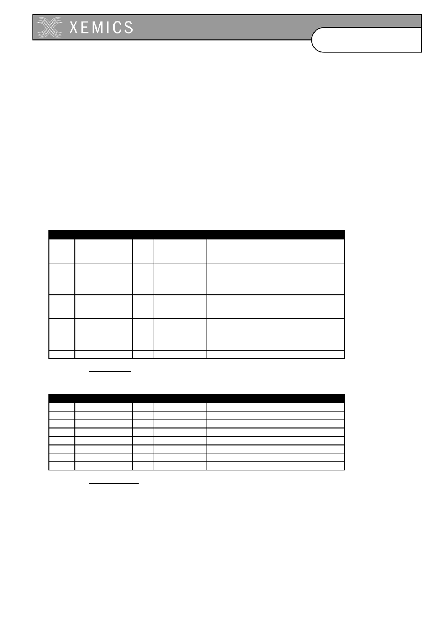
6-2
D0304-40
Datasheet
XE88LC05/05A
6.1 Features
∑
Power On Reset (POR)
∑
External reset from the RESET pin
∑
Programmable Watchdog timer reset
∑
Programmable BusError reset
∑
Sleep mode management
∑
Programmable Port A input combination reset
6.2 Overview
The reset block is the reset manager. It handles the different reset sources and distributes them
through the system. It also controls the sleep mode of the circuit.
6.3 Register
map
Pos.
RegSysCtrl
Rw
Reset
Function
7
SleepEn
r w
0 resetcold
enables Sleep mode
0: sleep mode is disabled
1: sleep mode is enabled
6
EnResPConf
r w
0 resetcold
enables the resetpconf signal when the
resetglobal is active
0: resetpconf is disabled
1: resetpconf is enabled
5
EnBusError
r w
0 resetcold
enables reset from BusError
0: BusError reset source is disabled
1: BusError reset source is enabled
4
EnResWD
r w
0 resetcold
enables reset from Watchdog
0: Watchdog reset source is disabled
1: Watchdog reset source is enabled
this bit can not be set to 0 by SW
3 ≠ 0
-
r
0000
unused
Table 6-1. RegSysCtrl register.
Pos.
RegSysReset
Rw
Reset
Function
7
Sleep
rw
0 resetsystem
Sleep mode control (reads always 0)
6 -
r 0
unused
5
ResetBusError
r c
0 resetcold
reset source was BusError
4
ResetWD
r c
0 resetcold
reset source was Watchdog
3
ResetfromportA
r c
0 resetcold
reset source was Port A combination
2
ResPad
r c
0 resetcold
reset source was reset pad
1
ResPadSleep
r c
0 resetcold
reset source was reset pad in sleep mode
0 -
r 0
unused
Table 6-2. RegSysReset register
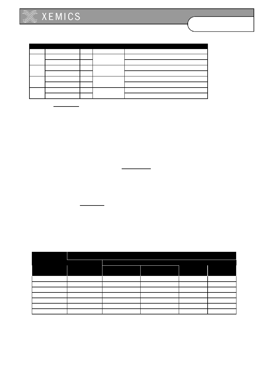
6-3
D0304-40
Datasheet
XE88LC05/05A
Pos.
RegSysWD
Rw
Reset
Function
7 ≠ 4
-
r
0000
unused
WDKey[3] w
Watchdog Key bit 3
3
WDCounter[3] r
0 resetcold
Watchdog counter bit 3
WDKey[2] w
Watchdog Key bit 2
2
WDCounter[2] r
0 resetcold
Watchdog counter bit 2
WDKey[1] w
Watchdog Key bit 1
1
WDCounter[1] r
0 resetcold
Watchdog counter bit 1
WDKey[0] w
Watchdog Key bit 0
0
WDCounter[0] r
0 resetcold
Watchdog counter bit 0
Table 6-3. RegSysWD register
6.4 Reset handling capabilities
There are 5 reset sources:
∑ Power On Reset (POR)
∑ External reset from the RESET pin
∑ Programmable Port A input combination
∑ Programmable watchdog timer reset
∑ Programmable BusError reset on processor access outside the allocated memory map
Another reset source is the bit Sleep in the RegSysReset register. This source is fully controlled by
software and is only used during the sleep mode.
Four internal reset signals are generated from these sources and distributed through the system:
∑ resetcold:
is asserted on POR
∑ resetsystem: is asserted when resetcold or any other enabled reset source is active
∑ resetpconf: is asserted when resetsystem is active and if the
EnResPConf bit in the
RegSysCtrl register is set. This reset is generally used in the different ports.
It allows to maintain the port configuration unchanged while the rest of the
circuit is reset.
∑ resetsleep: is asserted when the circuit is in sleep mode
For the
circuits XE88LC01A and XE88LC05A
(2) For the circuits XE88LC01 and XE88LC05
Table 6-4 shows a summary of the dependency of the internal reset signals on the various reset
sources. In all the tables describing the different registers, the reset source is indicated.
Internal reset signals
resetpconf
Asserted
reset source
resetsystem
when
EnResPConf=0
when
EnResPConf=1
resetsleep
resetcold
POR Asserted
Asserted
Asserted
Asserted
Asserted
RESET pin (1)
Asserted
Asserted Asserted
Asserted
Asserted
RESET pin (2)
Asserted
-
Asserted
-
-
PortA input
Asserted
-
Asserted
-
-
Watchdog Asserted
-
Asserted -
-
BusError Asserted -
Asserted - -
Sleep -
- -
Asserted
-
(1) For the circuits XE88LC01A and XE88LC05A
(2) For the circuits XE88LC01 and XE88LC05
Table 6-4. Internal reset assertion as a function of the reset source.

6-4
D0304-40
Datasheet
XE88LC05/05A
6.5 Reset source description
6.5.1
Power On Reset
The power on reset (POR) monitors the external supply voltage. It activates a reset on a rising edge
of this supply voltage. The reset is inactivated only if the internal voltage regulator has started up. No
precise voltage level detection is performed by the POR block.
6.5.2 RESET
pin
The reset can be activated by applying a high input state on the RESET pin.
6.5.3
Programmable Port A input combination
A reset signal can be generated by Port A. See the description of the Port A for further information.
6.5.4 Watchdog
reset
The Watchdog will generate a reset if the
EnResetWD
bit in the RegSysCtrl register has been set and
if the watchdog is not cleared in time by the processor. See chapter 6.7 describing the watchdog for
further information.
6.5.5 BusError
reset
The address space is assigned as shown in the register map of the product. If the
EnBusError
bit in
the RegSysCtrl register is set and a non-existant address is accessed by the software, a reset is
generated.
6.5.6 Sleep
mode
Entering the sleep mode will reset a part of the circuit. The reset is used to configure the circuit for
correct wake-up after the sleep mode. If the SleepEn bit in the RegSysCtrl register has been set, the
sleep mode can be entered by setting the bit Sleep in RegSysReset. During the sleep mode, the
resetsleep signal is active. For detailed information on the sleep mode, see the system
documentation.
6.6 Control register description and operation
Two registers are dedicated for reset status and control, RegSysReset and RegSysCtrl. The bits
Sleep, and SleepEn are also located in those registers and are described in the chapter dedicated to
the different operating modes of the circuit (system block).
The RegSysReset register gives information on the source which generated the last reset. It can be
read at the beginning of the application program to detect if the circuit is recovering from an error or
exception condition, or if the circuit is starting up normally.
∑ when ResBusError is 1, a forbidden address access generated the reset.
∑ when ResWD is 1, the watchdog generated the reset.
∑ when ResPortA is 1, a PortA combination generated the reset.
∑ when ResPad is 1, a reset pin generated the reset.
∑ when ResPadSleep is 1, a reset pin in sleep mode generated the reset.
Note: If no bit is set to 1, the reset source was the internal POR.
Note: Several bits might be set or not, if the register was not cleared in between 2 reset
occurrences. Write any value in RegSysReset to clear it.

6-5
D0304-40
Datasheet
XE88LC05/05A
Note: When a reset pin wakes up the chip from the sleep mode, ResPad and ResPadSleep
bits are equal at 1.
The last bit concerns the sleep mode control (see system documentation for the sleep mode
description).
∑ when Sleep is set to 1, and SleepEn is 1, the sleep mode is entered. The bit always reads
back a 0.
The RegSysCtrl register enables the different available reset sources and the sleep mode.
∑ EnResWD enables the reset due to the watchdog (can not be disabled once enabled).
∑ EnBusError enables the reset due to a bus error condition.
∑ EnResPConf enables the reset of the port configurations when reset by Port A, a Bus Error
or the watchdog.
∑ SleepEn unlocks the Sleep bit. As long as SleepEn is 0, the Sleep bit has no effect.
6.7 Watchdog
The watchdog is a timer which has to be cleared at least every 2 seconds by the software to prevent a
reset being generated by the timeout condition.
The watchdog can be enabled by software by setting the EnResWD bit in the RegSysCtrl register to
1. It can then only be disabled by a power on reset.
The watchdog timer can be cleared by writing consecutively the values Hx0A and Hx03 to the
RegSysWD register. The sequence must strictly be respected to clear the watchdog.
In assembler code, the sequence to clear the watchdog is:
move AddrRegSysWD, #0x0A
move AddrRegSysWD, #0x03
Only writing Hx0A followed by Hx03 resets the WD. If some other write instruction is done to the
RegSysWD between the writing of the Hx0A and Hx03 values, the watchdog timer will not be cleared.
It is possible to read the status of the watchdog in the RegSysWD register. The watchdog is a 4 bit
counter with a count range between 0 and 7. The system reset is generated when the counter is
reaching the value 8.
6.8 Start-up and watchdog specifications
At start-up of the circuit, the POR (power-on-reset) block generates a reset signal during t
POR
. The
circuit starts software execution after this period (see system chapter). The POR is intended to force
the circuit in a correct state at start-up. For precise monitoring of the supply voltage, the voltage level
detector (VLD) has to be used.

6-6
D0304-40
Datasheet
XE88LC05/05A
Symbol
Parameter
Min
Typ
Max
Unit
Comments
T
POR
POR reset duration
5
20
ms
T
RESET
RESET pin reset duration
20
200
µs
3
T
RESET
RESET pin reset duration
5
20
ms
4
Vbat_sl_M Supply ramp up of MTP version
20
V/ms
1
Vbat_sl_R
Supply ramp up of ROM version
0.25
V/ms
1
WDtime
Watchdog timeout period
2
s
2
Table 6-5. Electrical and timing specifications
Note: 1) The Vbat_sl defines the minimum slope required on VBAT. Correct start-up of the circuit is
not guaranteed if this slope is too slow. In such a case, a delay has to be built using the RESET pin.
Note: 2) The minimal watchdog timeout period is guaranteed when the internal oscillators are used.
The watchdog takes its clock from the low prescaler. In case an external clock source is used, the RC
oscillator must be enabled also (EnRC=1 in RegSysClock). Otherwise, the watchdog is stopped (see
the clock block documentation).
Note: 3) For the circuit versions XE88LC01 and XE88LC05. Gives the time the reset is active after
the falling edge of the RESET pin.
Note: 4) For the circuit versions XE88LC01A and XE88LC05A. Gives the time the reset is active after
the falling edge of the RESET pin.

7-1
clock_gen_ff - 1.0 ≠ 19 august 2002
D0304-40
Datasheet
XE88LC05/05A
7 Clock
Generator
7.1
Features
7-2
7.2
Overview
7-2
7.3
Register map
7-2
7.4
Interrupts and events map
7-3
7.5
Clock sources
7-4
7.5.1
RC oscillator
7-4
7.5.2
Xtal oscillator
7-6
7.5.3
External clock
7-7
7.6
Clock source selection
7-8
7.7
RegSysMisc Description
7-8
7.8
Prescalers
7-9
7.9
32 kHz frequency selector
7-9

7-2
D0304-40
Datasheet
XE88LC05/05A
7.1 Features
∑
3 available clock sources (RC oscillator, quartz oscillator and external clock).
∑
2 divider chains: high-prescaler (8 bits) and low-prescaler (15 bits).
∑
CPU clock disabling in halt mode.
7.2 Overview
The XE88LC05 chips can work on different clock sources (RC oscillator, quartz oscillator and external
clock). The clock generator block is in charge of distributing the necessary clock frequencies to the
circuit. Figure 7-1 represents the functionality of the clock block.
The internal RC oscillator drives the high prescaler. This prescaler generates frequency divisions
down to 1/256 of its input frequency. A 32kHz clock is generated by enabling the quartz oscillator (if
present in the product) or by selecting the appropriate tap on the high prescaler. The low prescaler
generates clock signals from 32kHz down to 1Hz. The clock source for the CPU can be selected from
the RC oscillator, the external clock or the 32kHz clock.
7.3 Register
map
pos.
RegSysClock
rw
Reset
function
7
CpuSel
rw 0 resetsleep Select speed for cpuck, 0=RC, 1=xtal or
external clock
6 Extclk
r 0
resetcold
External clock detected, 1=available
5
EnExtClock
rw
0 resetcold
Enable for external clock, 1=enabled
4
BiasRc
rw
1 resetcold
Enable Rcbias (reduces start-up time of RC).
3
ColdXtal
r
1 resetsleep
Xtal in start phase
2
ColdRC
r
1 resetsleep
RC in start phase
1
EnableXtal
rw
0 resetsleep
Enable Xtal oscillator, 0=disabled, 1=enabled
0
EnableRc
rw
1 resetsleep
Enable RC oscillator, 0=disabled, 1=enabled
Table 7-1: RegSysClock register
pos.
RegSysMisc
rw
Reset
Function
7-4 --
r 0000
Unused
3
RCOnPA0
rw
0 resetsleep
Start RC on PA[0], 0=disabled, 1=enabled
2 DebFast
rw
0
resetsleep
Debouncer clock speed, 0=256Hz, 1=8kHz
1 OutputCkXtal rw
0
resetsleep
Output Xtal Clock on PB[3], 0=disabled,
1=enabled if EnXtal=1 else PB[3]=0
0 OutputCpuCk rw
0
resetsleep
Output CPU clock on PB[2], 0=disabled,
1=enabled
Table 7-2: RegSysMisc register
pos.
RegSysPre0
rw
reset
Function
7-1 --
r 0000000
Unused
0 ResPre
w1
r0
0
Write 1 to reset low prescaler, but always
reads 0
Table 7-3: RegSysPre0 register
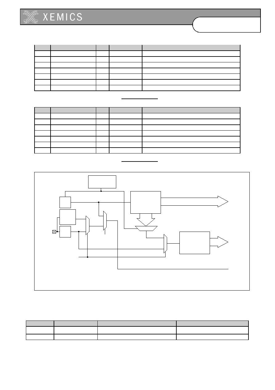
7-3
D0304-40
Datasheet
XE88LC05/05A
pos.
RegSysRcTrim1
rw
reset
Function
7-4 --
r 00
Unused
5 Reserved
rw
0
resetcold
Reserved
4
RcFreqRange
rw
0 resetcold
Low/high freq. range (low=0)
3
RcFreqCoarse[3]
rw
0 resetcold
RC coarse trim bit 3
2
RcFreqCoarse[2]
rw
0 resetcold
RC coarse trim bit 2
1
RcFreqCoarse[1]
rw
0 resetcold
RC coarse trim bit 1
0
RcFreqCoarse[0]
rw
0 resetcold
RC coarse trim bit 0
Table 7-4: RegSysRCTrim1 register
pos.
RegSysRcTrim2
Rw
reset
function
7-6 --
r 00
Unused
5
RcFreqFine[5]
rw
1 resetcold
RC fine trim bit 5
4
RcFreqFine[4]
rw
0 resetcold
RC fine trim bit 4
3
RcFreqFine[3]
rw
0 resetcold
RC fine trim bit 3
2
RcFreqFine[2]
rw
0 resetcold
RC fine trim bit 2
1
RcFreqFine[1]
rw
0 resetcold
RC fine trim bit 1
0
RcFreqFine[0]
rw
0 resetcold
RC fine trim bit 0
Table 7-5: RegSysRCTrim2 register
OSCIN
RC
Xtal
High prescaler
CpuCk
CpuSel
0
1
RegSysRcTrim1
RegSysRcTrim2
0
1
CkRc
CkXtal
EnXtal and
not(ExtClk or EnExtClk)
Low prescaler
32kHz
to
1Hz
CkRc
to
CkRc/256
External
Clock
0
1
Figure 7-1. Clock block structure
7.4 Interrupts and events map
Interrupt
Interrupt source
Mapping in the interrupt manager Mapping in the event manager
IrqPre1 Ck128Hz
RegIrqHig(6)
RegEvn(5)
IrqPre2 Ck1Hz
RegIrqMid(3)
RegEvn(1)
Table 7-6: Interrupts and events map

7-4
D0304-40
Datasheet
XE88LC05/05A
7.5 Clock
sources
7.5.1 RC
oscillator
7.5.1.1 Configuration
The RC oscillator is always turned on and selected for CPU and system operation at power-on reset
and when exiting sleep mode. It can be turned off after the Xtal (quartz oscillator) has been started,
after selection of the external clock or by entering sleep mode.
The RC oscillator has two frequency ranges: sub-MHz (100 kHz to 1 MHz) and above-MHz (1 MHz to
10 MHz). Inside a range, the frequency can be tuned by software for coarse and fine adjustment. See
registers RegSysRcTrim1 and RegSysRcTrim2.
Bit EnableRC in register RegSysClock controls the propagation of the RC clock signal and the
operation of the oscillator. The user can stop the RC oscillator by resetting the bit EnableRC. Entering
the sleep mode disables the RC oscillator.
Note: Before turning off the RC oscillator, the cpusel bit in RegSysClock must be set to one.
Note: The RC oscillator bias can be maintained while the oscillator is switched off by setting the bit
BiasRc in RegSysClock. This allows a faster restart of the RC oscillator at the cost of increased
power consumption when the oscillator is disabled (see section 7.5.1.3).
7.5.1.2
RC oscillator frequency tuning
The RC oscillator frequency can be set using the bits in the RegSysRcTrim1 and RegSysRcTrim2
registers. Figure 7-2 shows the nominal frequency of the RC oscillator as a function of these bits. The
absolute value of the frequency for a given register content may change by
±
50% from chip to chip
due to the tolerances on the integrated capacitors and resistors. However, the modification of the
frequency as a function of a modification of the register content is fairly precise for frequencies below
2MHz. This means that the curves in Figure 7-2 can shift up and down but that the slope remains
unchanged.
The bit RcFreqRange modifies the oscillator frequency by a factor of 10. The upper curve in the
figure corresponds to RcFreqRange=1.
The RcFreqCoarse modifies the frequency of the oscillator by a factor (RcFreqCoarse+1). The figure
represents the frequency for 5 different values of the bits RcFreqCoarse: for each value the
frequency is multiplied by 2.
Incrementing the RcFreqFine code increases the frequency by about 1.4%.
The frequency of the oscillator is therefor given by:
f
RC
=f
Rcmin
(1+9
RcFreqRange)
(1+RcFreqCoarse)
(1.014)
RcFreqFine
with f
Rcmin
the RC oscillator frequency if the registers are all 0. At higher frequencies, the frequency
may deviate from the value predicted by the equation.
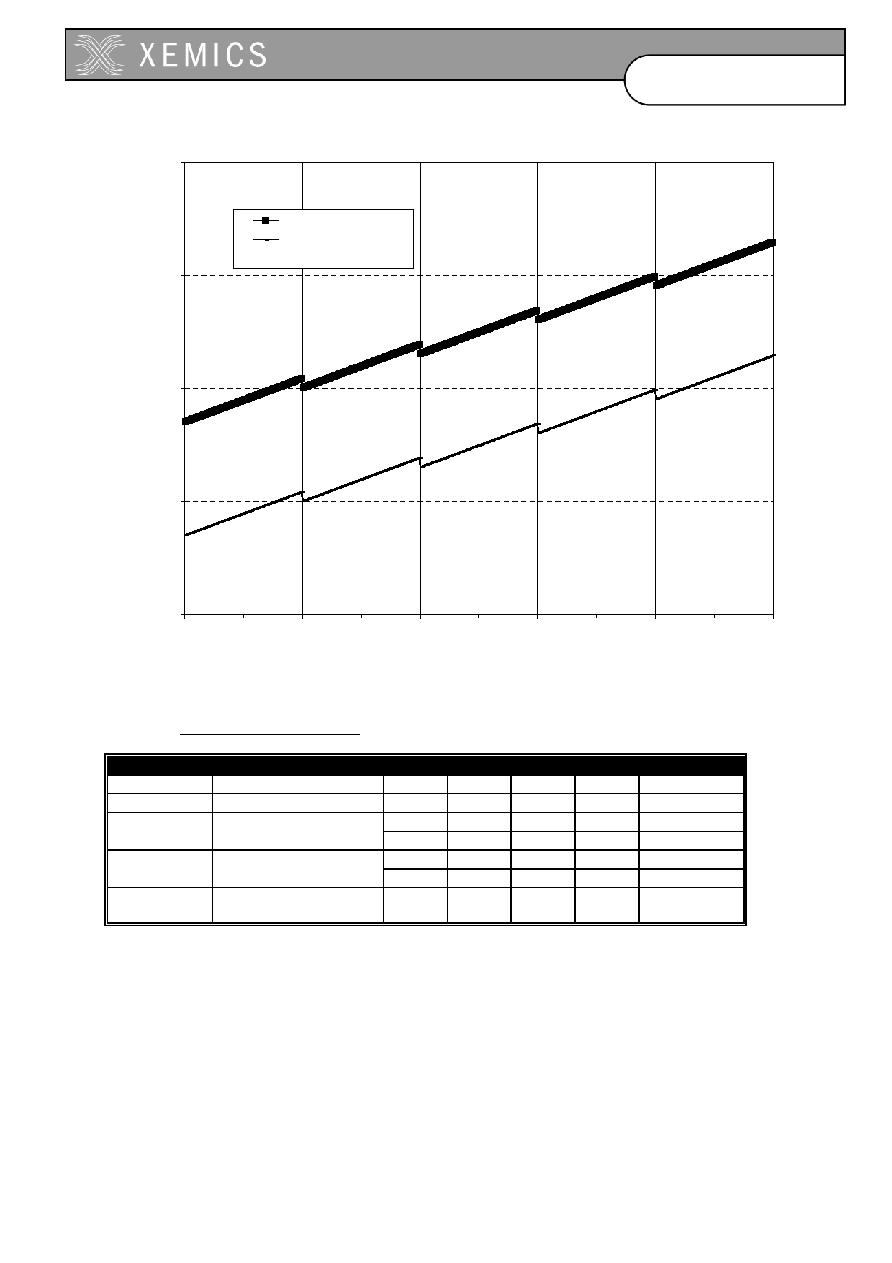
7-5
D0304-40
Datasheet
XE88LC05/05A
00
00
00
01
00
00
10
00
00
11
00
00
11
11
11
01
00
00
10
000
0
11
000
0
11
11
11
01
00
00
100
00
0
11
00
00
11
11
11
010
00
0
10
00
00
11
00
00
11
11
11
01
00
00
10
00
00
11
00
00
11
11
11
00
000
0
01
00
00
100
00
0
11
00
00
11
111
1
01
000
0
10
00
00
11
00
00
11
11
11
01
00
00
10
00
00
11
00
00
11
11
11
01
00
00
10
00
00
11
00
00
11
11
11
01
00
00
10
000
0
11
00
00
11
11
11
0000
0001
0011
0111
1111
1E+04
1E+05
1E+06
1E+07
1E+08
RcFreqCoarse(3:0)
Nominal RC oscillator frequency [Hz]
RcFreqRange='1'
RcFreqRange='0'
RcFreqFine(5:0)
RcFreqFine(5:0)
Figure 7-2. RC oscillator nominal frequency tuning.
7.5.1.3
RC oscillator specifications
symbol
description
min
typ
max
unit
Comments
f
RCmin
Lowest RC frequency
40
80
120
kHz
Note 1
RcFreqFine
fine tuning step
1.4
2.0
%
RC_su startup
time
30
50
us
BiasRc=0
3
5
us
BiasRc=1
PSRR @ DC Supply voltage
TBD
%/V
Note 2
dependence
TBD
%/V
Note
3
f/
T
Temperature
dependence
0.1
%/
∞
C
Table 7-7. RC oscillator specifications
Note 1: this is the frequency tolerance when all trimming codes are 0.
Note 2: frequency shift as a function of VBAT with normal regulator function.
Note 3: frequency shift as a function of VBAT while the regulator is short-circuited to VBAT.
The tolerances on the minimal frequency and the drift with supply or temperature can be cancelled
using the software DFLL (digital frequency locked loop) which uses the crystal oscillator as a
reference frequency.
7-6
D0304-40
Datasheet
XE88LC05/05A
7.5.2 Xtal
oscillator
7.5.2.1 Xtal
configuration
The Xtal operates with an external crystal of 32'768 Hz.
During Xtal oscillator start-up, the first 32768 cycles are masked. The two bits EnableXtal and
ColdXtal in register RegSysClock control the oscillator.
At power-on reset or during sleep mode, EnableXtal is reset and ColdXtal is set (Xtal oscillator is not
selected at start-up). The user can start Xtal oscillator by setting EnableXtal. When the Xtal oscillator
starts, bit ColdXtal is reset after 32768 cycles. Before ColdXtal is reset by the system, the Xtal
frequency precision is not guaranteed. The Xtal oscillator can be stopped by the user by resetting bit
EnableXtal.
When the user enters into sleep mode, the Xtal is stopped.
When an external clock is detected (ExtClk = 1) or the EnExtClock is set 1, the EnableXtal bit can
not be set to 1.
7.5.2.2
Xtal oscillator specifications
The crystal oscillator has been designed for a crystal with the specifications given in Table 7-8. The
oscillator precision can only be guaranteed for this crystal.
Symbol
Description
Min
Typ
Max
Unit
Comments
Fs Resonance
frequency
32768
Hz
CL
CL for nominal
frequency
8.2 15
pF
Rm Motional
resistance 40 100
k
Cm Motional
capacitance 1.8 2.5 3.2
fF
C0 Shunt
capacitance
0.7 1.1 2.0
pF
Rmp Motional
resistance
of
6
th
overtone (parasitic)
4 8
k
Q Quality
factor
30k
50k
400k
-
Table 7-8. Crystal specifications.
For safe operation, low power consumption and to meet the specified precision, careful board layout
is required:
Keep lines OSCIN and OSCOUT short and insert a VSS line in between them.
Connect the crystal package to VSS.
No noisy or digital lines near OSCIN or OSCOUT.
Insert guards where needed.
Respect the board specifications of Table 7-9.
Symbol
Description
Min
Typ
Max
Unit
Comments
Rh_oscin
Resistance OSCIN-VSS
10
M
Rh_oscout
Resistance OSCOUT-VSS
10
M
Rh_
oscin_oscout
Resistance OSCIN-OSCOUT
50
M
Cp_oscin
Capacitance OSCIN-VSS
0.5 3.0
pF
Cp_oscout
Capacitance OSCOUT-VSS
0.5 3.0
pF
Cp_
oscin_oscout
Capacitance OSCIN-OSCOUT
0.2 1.0
pF
Table 7-9. Board layout specifications.

7-7
D0304-40
Datasheet
XE88LC05/05A
The oscillator characteristics are given in Table 7-10. The characteristics are valid only if the crystal
and board layout meet the specifications above.
Symbol
Description
Min
Typ
Max
Unit
Comments
f
Xtal
Nominal frequency
32768
Hz
St_xtal Start-up
time
1
2
s
Fstab
Frequency deviation
-100
300
ppm
Note 1
Table 7-10. Crystal oscillator characteristics.
Note 1. This gives the relative frequency deviation from nominal for a crystal with CL=8.2pF and
within the temperature range -40
∞
C to 85
∞
C. The crystal tolerance, crystal aging and crystal
temperature drift are not included in this figure.
7.5.3 External
clock
7.5.3.1
External clock configuration
The user can provide an external clock instead of the internal oscillators. Only the CPU can use the
external clock. The external clock input pin is OSCIN.
The system is configured for external clock by bit EnExtClock in register RegSysClock.
When EnExtClock is set to 1, the external clock is detected after 4 pulses on pin OSCIN. The ExtClk
bit shows when the external clock is available.
Note: when using the external clock, the Xtal is not available.
7.5.3.2
External clock specification
The external clock has to satisfy the specifications in the table below. Correct behavior of the circuit
can not be guaranteed if the external clock signal does not respect the specifications below.
Symbol
Description
Min
Typ
Max
Unit
Comments
F
EXT
External clock
frequency
2
MHz
PW_1
Pulse 1 width
0.2
µ
s
PW_0
Pulse 0 width
0.2
µ
s
Table 7-11. External clock specifications.
7-8
D0304-40
Datasheet
XE88LC05/05A
7.6 Clock source selection
There are three possible clock sources available for the CPU clock. The RC clock is always selected
after power-up or after Sleep mode. The CPU clock selection is done with the bit CpuSel in
RegSysClock (0= RC clock, 1= 32 kHz from Xtal if EnableXtal =1, ExtClk = 0 and EnExtClk = 0
else external clock).
Switching from one clock source to another is glitch free.
The next table summarizes the different clock configurations of the circuit:
Clock Sources
Clock targets
Cpuck
Note 1
Mode
name
EnExtClk
EnableRc
EnableXtal
CpuSel=0
CpuSel=1
High
Prescaler
Clock
input
Low
Prescaler
Clock
input
Sleep
0 0 0
Off
Off
Off
Off
Xtal
0 0 1
Off
Xtal
Off
Xtal
RC
0 1 0
RC
RC RC
High
presc.
RC + Xtal
0 1 1
RC
Xtal RC
Xtal
External 1 0 X Off External Off
Off
RC +
External
1 1 X
RC
External RC High
presc.
Table 7-12: Table of clocking modes.
Note 1: The CPU clock can be divided by using the freq instruction (see coolrisc instruction set)
Switching from one clock source to another and stopping the unused clock source must be performed
using 3 MOVE instructions to RegSysClock. First select the new clock source, secondly change the
CpuSel bit and finally stop the unused one.
7.7 RegSysMisc
Description
The RCOnPA0 bit in RegSysMisc can be used to enable the RC oscillator on an event external to
the circuit. If RCOnPA0 is 1, the RC oscillator is enabled (EnableRC bit is set to 1) as soon as the
value on port A pin PA[0] is equal to 1. The port A pin can be debounced (see port A documentation).
Bit DebFast in the RegSysMisc register allows to chose the debouncer clock between 256Hz and
8kHz (DebFast = 0 and DebFast = 1 respectively). The Debouncer clock is used to debounce PA
inputs (see port A documentation).
Bit OutputCkXtal allows to show the Xtal clock on PB[3]. The EnableXtal bit must be set to 1 else
PB[3] equals 0 (see port B documentation to set up the port B).
Bit OutputCpuCk allows to show the CpuClock on PB[2] (see port B documentation).

7-9
D0304-40
Datasheet
XE88LC05/05A
7.8 Prescalers
The clock generator block embeds two divider chains: the high prescaler and the low prescaler.
The high prescaler is made of an 8 stage dividing chain and the low prescaler of a 15 stage dividing
chain.
Features:
∑
High prescaler can only be driven with RC clock (bit EnableRc have to be set, see Table 7-12).
∑
Low prescaler can be driven from the high prescaler or directly with the Xtal clock when bit
EnableXtal is set to 1, bit EnExtClock is set to 0 and ExtClk is equal at 0.
∑
Bit
ResPre in the RegSysPre0 register allows to reset synchronously the low prescaler, the low
prescaler is also automatically cleared when bit EnableXtal is set. Both dividing chains are reset
asynchronously by the resetsleep signal.
∑
Bit
ColdXtal=1 indicates the Xtal is in its start up phase. It is active for 37268 Xtal cycles after
setting EnableXtal.
7.9 32 kHz frequency selector
A decoder is used to select from the high prescaler the frequency tap that is the closest to 32 kHz to
operate the low prescaler when the Xtal is not running. In this case, the RC oscillator frequency of
±
50% will also be valid for the low prescaler frequency outputs.

8-1
irq_ff - 1.0 ≠ 28 august 2002
D0304-40
Datasheet
XE88LC05/05A
8 IRQ - Interrupt handler
8.1
Features
8-2
8.2
Overview
8-2
8.3
Register map
8-2
8-2
D0304-40
Datasheet
XE88LC05/05A
8.1 Features
The XE8000 chips support 24 interrupt sources, divided into 3 levels of priority.
8.2 Overview
A CPU interruption is generated and memorized when an interrupt becomes active. The 24 interrupt
sources are divided into 3 levels of priority: High (8 interrupt sources), Mid (8 interrupt sources), and
Low (8 interrupt sources). Those 3 levels of priority are directly mapped to those supported by the
CoolRiscÆ (IN0, IN1 and IN2; see CoolRiscÆ documentation for more information).
RegIrqHig, RegIrqMid, and RegIrqLow are 8-bit registers containing flags for the interrupt sources.
Those flags are set when the interrupt is enabled (i.e. if the corresponding bit in the registers
RegIrqEnHig, RegIrqEnMid or RegIrqEnLow is set) and a rising edge is detected on the
corresponding interrupt source.
Once memorized, an interrupt flag can be cleared by writing a `1' in the corresponding bit of
RegIrqHig, RegIrqMid or RegIrqLow. Writing a `0' does not modify the flag. To definitively clear the
interrupt, one has to clear the CoolRisc interrupt in the CoolRisc status register. All interrupts are
automatically cleared after a reset.
Two registers are provided to facilitate the writing of interrupt service software. RegIrqPriority
contains the number of the highest priority interrupt set (its value is 0xFF when no interrupt is set).
RegIrqIrq indicates the priority level of the current interrupts. RegIrqIrq and RegIrqPriority `s values
are dependent upon the memorized state of the interrupts (as reflected in flags in RegIrqHig,
RegIrqMid and RegIrqLow).
8.3 Register
map
pos.
RegIrqHig
rw
reset
function
7 RegIrqHig[7] r
c1
0 resetsystem
interrupt #23 (high priority)
clear interrupt #23 when 1 is written
6 RegIrqHig[6] r
c1
0 resetsystem
interrupt #22 (high priority)
clear interrupt #22 when 1 is written
5 RegIrqHig[5] r
c1
0 resetsystem
interrupt #21 (high priority)
clear interrupt #21 when 1 is written
4 RegIrqHig[4] r
c1
0 resetsystem
interrupt #20 (high priority)
clear interrupt #20 when 1 is written
3 RegIrqHig[3] r
c1
0 resetsystem
interrupt #19 (high priority)
clear interrupt #19 when 1 is written
2 RegIrqHig[2] r
c1
0 resetsystem
interrupt #18 (high priority)
clear interrupt #18 when 1 is written
1 RegIrqHig[1] r
c1
0 resetsystem
interrupt #17 (high priority)
clear interrupt #17 when 1 is written
0 RegIrqHig[0] r
c1
0 resetsystem
interrupt #16 (high priority)
clear interrupt #16 when 1 is written
Table 8-1: RegIrqHig

8-3
D0304-40
Datasheet
XE88LC05/05A
pos.
RegIrqMid
rw
reset
function
7 RegIrqMid[7] r
c1
0 resetsystem
interrupt #15 (mid priority)
clear interrupt #15 when 1 is written
6 RegIrqMid[6] r
c1
0 resetsystem
interrupt #14 (mid priority)
clear interrupt #14 when 1 is written
5 RegIrqMid[5] r
c1
0 resetsystem
interrupt #13 (mid priority)
clear interrupt #13 when 1 is written
4 RegIrqMid[4] r
c1
0 resetsystem
interrupt #12 (mid priority)
clear interrupt #12 when 1 is written
3 RegIrqMid[3] r
c1
0 resetsystem
interrupt #11 (mid priority)
clear interrupt #11 when 1 is written
2 RegIrqMid[2] r
c1
0 resetsystem
interrupt #10 (mid priority)
clear interrupt #10 when 1 is written
1 RegIrqMid[1] r
c1
0 resetsystem
interrupt #9 (mid priority)
clear interrupt #9 when 1 is written
0 RegIrqMid[0] r
c1
0 resetsystem
interrupt #8 (mid priority)
clear interrupt #8 when 1 is written
Table 8-2: RegIrqMid
pos.
RegIrqLow
rw
reset
function
7 RegIrqLow[7] r
c1
0 resetsystem
interrupt #7 (low priority)
clear interrupt #7 when 1 is written
6 RegIrqLow[6] r
c1
0 resetsystem
interrupt #6 (low priority)
clear interrupt #6 when 1 is written
5 RegIrqLow[5] r
c1
0 resetsystem
interrupt #5 (low priority)
clear interrupt #5 when 1 is written
4 RegIrqLow[4] r
c1
0 resetsystem
interrupt #4 (low priority)
clear interrupt #4 when 1 is written
3 RegIrqLow[3] r
c1
0 resetsystem
interrupt #3 (low priority)
clear interrupt #3 when 1 is written
2 RegIrqLow[2] r
c1
0 resetsystem
interrupt #2 (low priority)
clear interrupt #2 when 1 is written
1 RegIrqLow[1] r
c1
0 resetsystem
interrupt #1 (low priority)
clear interrupt #1 when 1 is written
0 RegIrqLow[0] r
c1
0 resetsystem
interrupt #0 (low priority)
clear interrupt #0 when 1 is written
Table 8-3: RegIrqLow
pos.
RegIrqEnHig
rw
reset
function
7
RegIrqEnHig[7]
rw
0 resetsystem
1= enable interrupt #23
6
RegIrqEnHig[6]
rw
0 resetsystem
1= enable interrupt #22
5
RegIrqEnHig[5]
rw
0 resetsystem
1= enable interrupt #21
4
RegIrqEnHig[4]
rw
0 resetsystem
1= enable interrupt #20
3
RegIrqEnHig[3]
rw
0 resetsystem
1= enable interrupt #19
2
RegIrqEnHig[2]
rw
0 resetsystem
1= enable interrupt #18
1
RegIrqEnHig[1]
rw
0 resetsystem
1= enable interrupt #17
0
RegIrqEnHig[0]
rw
0 resetsystem
1= enable interrupt #16
Table 8-4: RegIrqEnHig

8-4
D0304-40
Datasheet
XE88LC05/05A
pos.
RegIrqEnMid
rw
reset
function
7
RegIrqEnMid[7]
rw
0 resetsystem
1= enable interrupt #15
6
RegIrqEnMid[6]
rw
0 resetsystem
1= enable interrupt #14
5
RegIrqEnMid[5]
rw
0 resetsystem
1= enable interrupt #13
4
RegIrqEnMid[4]
rw
0 resetsystem
1= enable interrupt #12
3
RegIrqEnMid[3]
rw
0 resetsystem
1= enable interrupt #11
2
RegIrqEnMid[2]
rw
0 resetsystem
1= enable interrupt #10
1
RegIrqEnMid[1]
rw
0 resetsystem
1= enable interrupt #9
0
RegIrqEnMid[0]
rw
0 resetsystem
1= enable interrupt #8
Table 8-5: RegIrqEnMid
pos.
RegIrqEnLow
rw
reset
function
7
RegIrqEnLow[7]
rw
0 resetsystem
1= enable interrupt #7
6
RegIrqEnLow[6]
rw
0 resetsystem
1= enable interrupt #6
5
RegIrqEnLow[5]
rw
0 resetsystem
1= enable interrupt #5
4
RegIrqEnLow[4]
rw
0 resetsystem
1= enable interrupt #4
3
RegIrqEnLow[3]
rw
0 resetsystem
1= enable interrupt #3
2
RegIrqEnLow[2]
rw
0 resetsystem
1= enable interrupt #2
1
RegIrqEnLow[1]
rw
0 resetsystem
1= enable interrupt #1
0
RegIrqEnLow[0]
rw
0 resetsystem
1= enable interrupt #0
Table 8-6: RegIrqEnLow
pos.
RegIrqPriority
rw
reset
function
7-0 RegIrqPriority r 11111111
resetsystem
code of highest priority set
Table 8-7: RegIrqPriority
pos.
RegIrqIrq
rw
Reset
function
7-3 -
r 00000
unused
2
IrqHig
r
0 resetsystem
one or more high priority interrupt is
set
1
IrqMid
r
0 resetsystem
one or more mid priority interrupt is
set
0
IrqLow
r
0 resetsystem
one or more low priority interrupt is
set
Table 8-8: RegIrqIrq

9-1
evn_ff - 1.0 ≠ 28 august 2002
D0304-40
Datasheet
XE88LC05/05A
9 Event
handler
9.1
Features
9-2
9.2
Overview
9-2
9.3
Register map
9-2

9-2
D0304-40
Datasheet
XE88LC05/05A
9.1 Features
The XE8000 chips support 8 event sources, divided into 2 levels of priority.
9.2 Overview
A CPU event is generated and memorized when an event source becomes active. The 8 event
sources are divided into 2 levels of priority: High (4 event sources) and Low (4 event sources). Those
2 levels of priority are directly mapped to those supported by the CoolRisc (EV0 and EV1; see
CoolRisc documentation for more information).
RegEvn is an 8-bit register containing flags for the event sources. Those flags are set when the event
is enabled (i.e. if the corresponding bit in the registers RegEvnEn is set) and a rising edge is detected
on the corresponding event source.
Once memorized, writing a `1' in the corresponding bit of RegEvn clears an event flag. Writing a `0'
does not modify the flag. All interrupts are automatically cleared after a reset.
Two registers are provided to facilitate the writing of event service software. RegEvnPriority contains
the number of the highest priority event set (its value is 0xFF when no event is set). RegEvnEvn
indicates the priority level of the current interrupts. RegEvnEvn and RegEvnPriority `s values are
dependent upon the memorized state of the events (as reflected in flags in RegEvn).
9.3 Register
map
pos.
RegEvn
rw
reset
function
7 RegEvn[7]
r
c1
0 resetsystem
event #7 (high priority)
clear event #7 when written 1
6 RegEvn[6]
r
c1
0 resetsystem
event #6 (high priority)
clear event #6 when written 1
5 RegEvn[5]
r
c1
0 resetsystem
event #5 (high priority)
clear event #5 when written 1
4 RegEvn[4]
r
c1
0 resetsystem
event #4 (high priority)
clear event #4 when written 1
3 RegEvn[3]
r
c1
0 resetsystem
event #3 (low priority)
clear event #3 when written 1
2 RegEvn[2]
r
c1
0 resetsystem
event #2 (low priority)
clear event #2 when written 1
1 RegEvn[1]
r
c1
0 resetsystem
event #1 (low priority)
clear event #1 when written 1
0 RegEvn[0]
r
c1
0 resetsystem
event #0 (low priority)
clear event #0 when written 1
Table 9-1: RegEvn

9-3
D0304-40
Datasheet
XE88LC05/05A
pos.
RegEvnEn
rw
reset
function
7
RegEvnEn[7]
rw
0 resetsystem
1= enable event #7
6
RegEvnEn[6]
rw
0 resetsystem
1= enable event #6
5
RegEvnEn[5]
rw
0 resetsystem
1= enable event #5
4
RegEvnEn[4]
rw
0 resetsystem
1= enable event #4
3
RegEvnEn[3]
rw
0 resetsystem
1= enable event #3
2
RegEvnEn[2]
rw
0 resetsystem
1= enable event #2
1
RegEvnEn[1]
rw
0 resetsystem
1= enable event #1
0
RegEvnEn[0]
rw
0 resetsystem
1= enable event #0
Table 9-2: RegEvnEn
pos.
RegEvnPriority
rw
reset
function
7-0 RegEvnPriority r 11111111
resetsystem
code of highest event set
Table 9-3: RegEvnPriority
pos.
RegEvnEvn
rw
reset
function
7-2 -
r 00000
unused
1
EvnHig
r
0 resetsystem
one or more high priority event is set
0
EvnLow
r
0 resetsystem
one or more low priority event is set
Table 9-4: RegEvnEvn

10-1
reg_ff - 1.0 ≠ 28 august 2002
D0304-40
Datasheet
XE88LC05/05A
10 Low power RAM
10.1
Features
10-2
10.2
Overview
10-2
10.3
Register map
10-2

10-2
D0304-40
Datasheet
XE88LC05/05A
10.1 Features
∑
Low power RAM locations.
10.2 Overview
In order to save power consumption, 8 8-bit registers are provided in page 0. These memory locations
should be reserved for often-updated variables. Accessing these register locations requires much less
power than the other general purpose RAM locations.
10.3 Register map
pos.
Reg00
rw
reset
function
7-0 Reg00
rw XXXXXXXX
low-power data memory
Table 10-1: Reg00
pos.
Reg01
rw
reset
function
7-0 Reg01
rw XXXXXXXX
low-power data memory
Table 10-2: Reg01
pos.
Reg02
rw
reset
function
7-0 Reg02
rw XXXXXXXX
low-power data memory
Table 10-3: Reg02
pos.
Reg03
rw
reset
function
7-0 Reg03
rw XXXXXXXX
low-power data memory
Table 10-4: Reg03
pos.
Reg04
rw
reset
function
7-0 Reg04
rw XXXXXXXX
low-power data memory
Table 10-5: Reg04
pos.
Reg05
rw
reset
function
7-0 Reg05
rw XXXXXXXX
low-power data memory
Table 10-6: Reg05
pos.
Reg06
rw
®reset
function
7-0 Reg06
rw XXXXXXXX
low-power data memory
Table 10-7: Reg06
pos.
Reg07
rw
reset
function
7-0 Reg07
rw XXXXXXXX
low-power data memory
Table 10-8: Reg07

11-1
pa_ff - 1.0 ≠ 16 may 2002
D0304-40
Datasheet
XE88LC05/05A
11 Port A
11.1
Features
11-2
11.2
Overview
11-2
11.3
Register map
11-3
11.4
Interrupts and events map
11-3
11.5
Port A (PA) Operation
11-4
11.6
Port A electrical specification
11-5

11-2
D0304-40
Datasheet
XE88LC05/05A
11.1 Features
∑
Input port, 8 bits wide
∑
Each bit can be set individually for debounced or direct input
∑
Each bit can be set individually for pull-up or not
∑
Each bit is an interrupt request source on the rising or falling edge
∑
A system reset can be generated on an input pattern
∑
PA[0] and PA[1] can generate two events for the CPU, individually maskable
∑
PA[0] to PA[3] can be used as clock inputs for the counters/timers/PWM (product dependent)
∑
PA[0] can be used to enable the RC oscillator
11.2 Overview
Port A is a general purpose 8 bit wide digital input port, with interrupt capability. Figure 11-1 shows its
structure.
Figure 11-1:structure of Port A
VBat
1
0
resetfromporta
8x
RegPAPullup
RegPADebounce
RegPAIn
RegPACtrl
RegPAEdge
RegPARes1
RegPARes0
0
1
8x
1
00
01
11
10
0
interrupts
events
cntclocks
8
8
8
8
8
debounce
1
0
DebFast
(RegSysMisc(2))
256 Hz
8 kHz
8
8
8
Port A
8x
PAReset[x]
RC
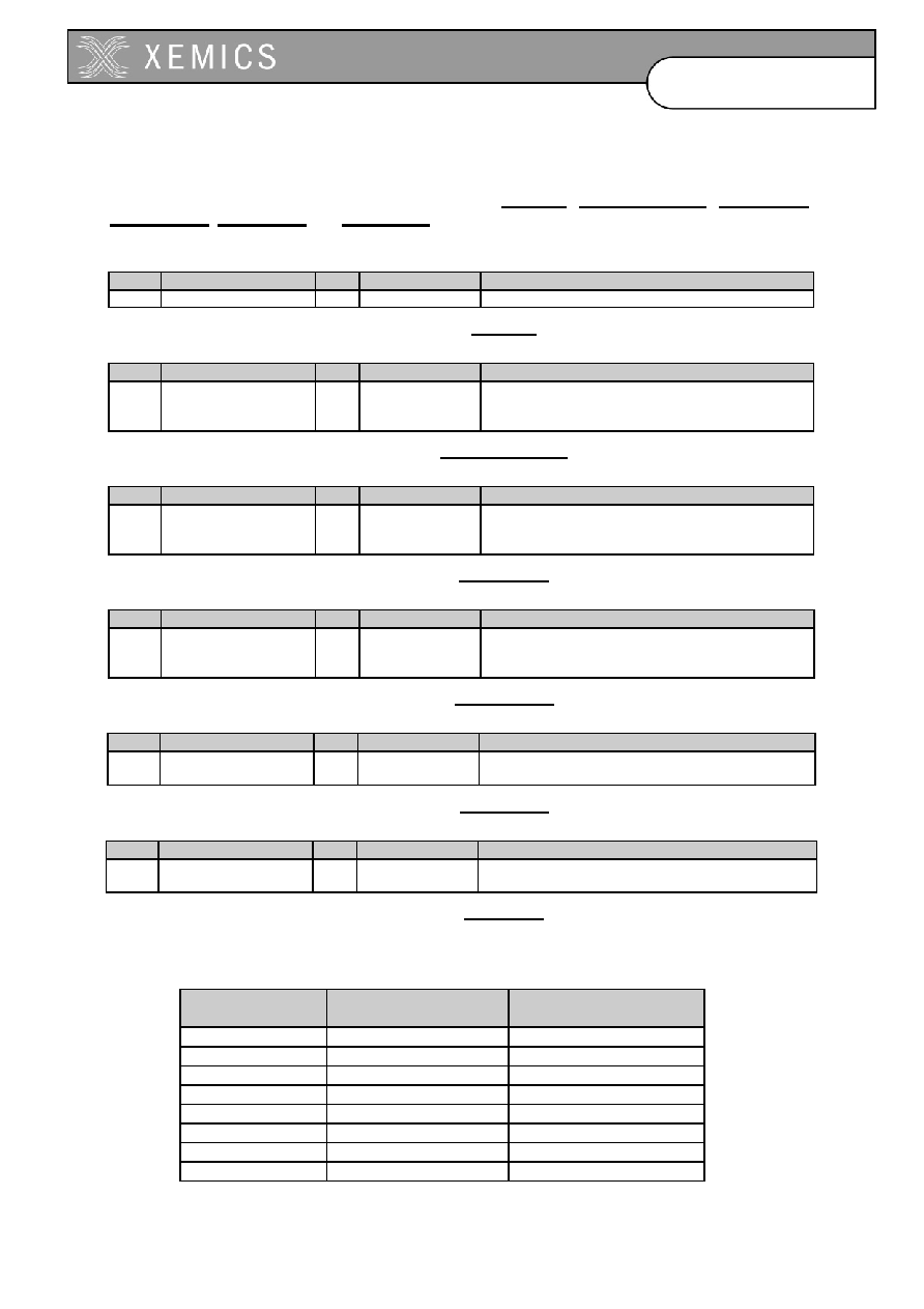
11-3
D0304-40
Datasheet
XE88LC05/05A
11.3 Register map
There are six registers in the Port A (PA), namely RegPAIn, RegPADebounce, RegPAEdge,
RegPAPullup, RegPARes0 and RegPARes1. Table 11-1 to Table 11-6 show the mapping of control
bits and functionality.
pos.
RegPAIn
rw
reset
description
7:0
PAIn[7:0]
r
pad PA[7] to PA[0] input value
Table 11-1: RegPAIn
pos.
RegPADebounce
rw
reset
description
7:0 PADebounce[7:0]
r
w
00000000
resetpconf
PA[7] to PA[0]
1: debounce enabled
0: debounce disabled
Table 11-2: RegPADebounce
pos.
RegPAEdge
rw
reset
description
7:0 PAEdge[7:0]
r
w
00000000
resetsystem
PA[7] to PA[0] edge configuration
0: positive edge
1: negative edge
Table 11-3: RegPAEdge
pos.
RegPAPullup
rw
reset
description
7:0 PAPullup[7:0]
r
w
00000000
resetpconf
PA[7] to PA[0] pullup enable
0: pullup disabled
1: pullup enabled
Table 11-4: RegPAPullup
pos.
RegPARes0
rw
Reset
description
7:0 PARes0[7:0]
r
w
00000000
resetsystem
PA[7] to PA[0] reset configuration
Table 11-5: RegPARes0
pos.
RegPARes1
rw
reset
Description
7:0 PARes1[7:0]
r
w 00000000
resetsystem
PA[7] to PA[0] reset configuration
Table 11-6: RegPARes
11.4 Interrupts and events map
Interrupt source
Default mapping in
the interrupt manager
Default mapping in the
event manager
pa_irqbus[5] RegIrqMid[5]
pa_irqbus[4] RegIrqMid[4]
pa_irqbus[1] RegIrqMid[1]
RegEvn[4]
pa_irqbus[0] RegIrqMid[0]
RegEvn[0]
pa_irqbus[7] RegIrqLow[7]
pa_irqbus[6] RegIrqLow[6]
pa_irqbus[3] RegIrqLow[3]
pa_irqbus[2] RegIrqLow[2]
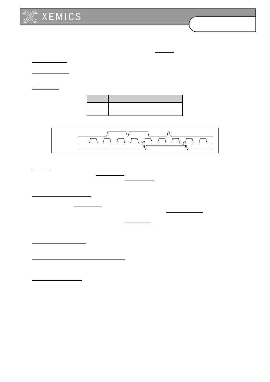
11-4
D0304-40
Datasheet
XE88LC05/05A
11.5 Port A (PA) Operation
The Port A input status (debounced or not) can be read from RegPAin.
Debounce mode:
Each bit in Port A can be individually debounced by setting the corresponding bit in
RegPADebounce. After reset, the debounce function is disabled. After enabling the debouncer, the
change of the input value is accepted only if the input value is identical at two consecutive sampling
on the rising edge of the selected clock. Selection of the clock is done by the bit DebFast in Register
RegSysMisc (see clock block documentation for more precision on the frequency).
DebFast
Clock filter
0 256
Hz
1 8
kHz
Table 11-7: debounce frequency selection
Figure 11-2: digital debouncer
Pull-ups:
When the corresponding bit in RegPAPullup is set to 0, the inputs are floating (pull-up resistors are
disconnected). When the corresponding bit in RegPAPullup is set to 1, a pull-up resistor is connected
to the input pin. Port A starts up with the pull-up resistors disconnected.
Port A as an interrupt source:
Each Port A input is an interrupt request source and can be set on rising or falling edge with the
corresponding bit in RegPAEdge. After reset, the rising edge is selected for interrupt generation by
default. The interrupt source can be debounced by setting register RegPADebounce.
Note: care must be taken when modifying RegPAEdge because this register performs an edge
selection. The change of this register may result in a transition which may be interpreted as a valid
interruption.
Port A as an event source:
The interrupt signals of the pins PA[0] and PA[1] are also available as events on the event controller.
Port A as a clock source (product dependent):
Images of the PA[0] to PA[3] input ports (debounced or not) are available as clock sources for the
counter/timer/PWM peripheral (see the counter block documentation for more information).
Port A as a reset source:
Port A can be used to generate a system reset by placing a predetermined word on Port A externally.
The reset is built using a logical and of the 8 PARes[x] signals:
resetfromportA = PAReset[7] AND PAReset[6] AND PAReset[5] AND ... AND PAReset[0]
Input
CkDebounce
Debounced
1
1
2
1
1
2

11-5
D0304-40
Datasheet
XE88LC05/05A
PAReset[x] is itself a logical function of the corresponding pin PA[x]. One of four logical functions can
be selected for each pin by writing into two registers RegPARes0 and RegPARes1 as shown in
Table 11-8.
PARes1[x]
PARes0[x]
PAReset[x]
0 0 0
0 1
PA[x]
1 0
not(PA[x])
1 1 1
Table 11-8: Selection bits for reset signal
A reset from Port A can be inhibited by placing a 0 on both PARes1[x] and PARes0[x] for at least 1
pin. Setting both PARes1[x] and PARes0[x] to 1, makes the reset independent of the value on the
corresponding pin. Setting both registers to hFF, will reset the circuit independent from the Port A
input value. This makes it possible to do a software reset.
Note: depending of the value of PA[0] to PA[7], the change of RegPARes0 and RegPARes1 can
cause a reset. Therefore it is safe to have always one (RegPARes0[x], RegPARes1[x]) equal to `00'
during the setting operations.
Port A as a RC enable:
PA[0] can be used to enable the RC oscillator. When RCOnPA0 bit in RegSysMisc is set to 1 and the
value of PA[0] (debounced or not) is equal to 1, the EnRc bit in RegSysClock is automatically set to
1.
11.6 Port A electrical specification
Sym
description
min
typ
max
unit Comments
V
INH
Input high voltage
0.7*VBAT
VBAT
V
VBAT
2.4V
V
INL
Input low voltage
VSS
0.2*VBAT
V
VBAT
2.4V
R
PU
Pull-up resistance
20
50
80
k
Cin
Input capacitance
3.5
pF
Note 1
Note 1: this value is indicative only since it depends on the package.
Table 11-9. Port A electrical specification.

12-1
pb_ff - 1.0 ≠ 02 september 2002
D0304-40
Datasheet
XE88LC05/05A
12 Port B
12.1
Features
12-2
12.2
Overview
12-2
12.3
Register map
12-2
12.4
Port B capabilities
12-3
12.5
Port B analog capability
12-3
12.5.1
Port B analog configuration
12-3
12.5.2
Port B analog function specification
12-4
12.6
Port B function capability
12-4
12.7
Port B digital capabilities
12-5
12.7.1
Port B digital configuration
12-5
12.7.2
Port B digital function specification
12-6
12-2
D0304-40
Datasheet
XE88LC05/05A
12.1 Features
∑ Input / output / analog port, 8 bits wide
∑ Each bit can be set individually for input or output
∑ Each bit can be set individually for open-drain or push-pull
∑ Each bit can be set individually for pull-up or not (for input or open-drain mode)
∑ In open-drain mode, pull-up is not active when corresponding pad is set to zero
∑ The 8 pads can be connected by pairs to four internal analog lines (4 line analog bus)
∑ Two internal freq. (cpuck and 32 kHz) can be output on PB[2] and PB[3]
Product dependant:
∑ Two PWM signal can be output on pads PB[0] and PB[1]
∑ The synchronous serial interface (USRT) uses pads PB[5], PB[4]
∑ The UART interface uses pads PB[6] and PB[7] for Tx and Rx
12.2 Overview
Port B is a multi-purpose 8 bit Input/output port. In addition to digital functions, all pins can be used for
analog signals. All port terminals can be selected by pairs as digital input or output or as analog to
share one of four possible analog lines.
12.3 Register map
Pos.
RegPBOut
rw
reset
description in digital mode
description in analog mode
7 ≠ 0
PBOut[7-0]
r w
0 resetpconf
Pad PB[7-0] output value
Analog bus selection for pad PB[7-0]
Table 12-1: RegPBOut
Pos.
RegPBIn
rw
reset
description in digital mode
description in analog mode
7 ≠ 0
PBIn[7-0]
r w
Pad PB[7-0] input status
Unused
Table 12-2: RegPBIn
Pos.
RegPBDir
rw
reset
description in digital mode
description in analog mode
7 ≠ 0
PBDir [7-0]
r w
0 resetpconf
Pad PB[7-0] direction (0=input)
Analog bus selection for pad PB[7-0]
Table 12-3: RegPBDir
Pos.
RegPBOpen
rw
reset
description in digital mode
description in analog mode
7 ≠ 0
PBOpen[7-0]
r w
0 resetpconf
Pad PB[7-0] open drain (1 = open
drain)
Unused
Table 12-4: RegPBOpen
Pos.
RegPBPullup
rw
reset
description in digital mode
description in analog mode
7 ≠0
PBPullup[7]
r w
0 resetpconf
Pull-up for pad PB[7-0] (1=active)
Connect pad PB[7-0] on selected ana
bus
Table 12-5: RegPBPullup
Pos.
RegPBAna
rw
reset
description in digital mode
description in analog mode
7 ≠ 4
--
r
0000
Unused
Unused
3
PBAna [3]
r w
0 resetpconf
Set PB[7:6] in analog mode
Set PB[7:6] in analog mode
2
PBAna [2]
r w
0 resetpconf
Set PB[5:4] in analog mode
Set PB[5:4] in analog mode
1
PBAna [1]
r w
0 resetpconf
Set PB[3:2] in analog mode
Set PB[3:2] in analog mode
0
PBAna [0]
r w
0 resetpconf
Set PB[1:0] in analog mode
Set PB[1:0] in analog mode
Table 12-6: RegPBAna
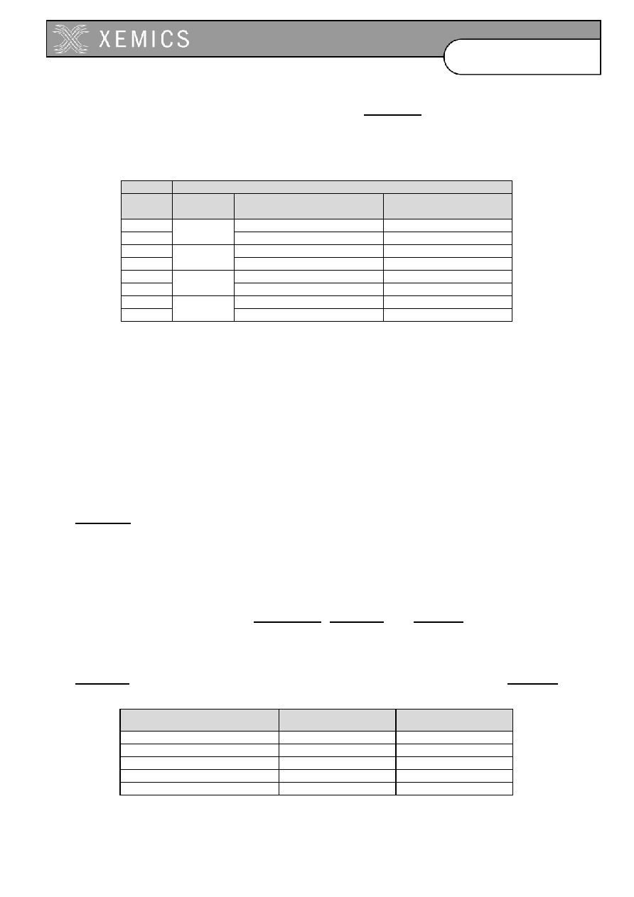
12-3
D0304-40
Datasheet
XE88LC05/05A
Note: Depending on the status of the EnResPConf bit in RegSysCtrl, the reset conditions of the
registers are different. See the reset block documentation for more details on the resetpconf signal.
12.4 Port B capabilities
Port B
usage (priority)
name
analog
(high)
functions
(medium)
digital
(low) (default)
PB[7] uart
Rx
I/O
PB[6]
analog
uart Tx
I/O
PB[5] usrt
S1
I/O
PB[4]
analog
usrt S0
I/O
PB[3] 32
kHz
I/O
PB[2]
analog
clock CPU
I/O
PB[1]
PWM1 Counter C (C+D)
I/O
PB[0]
analog
PWM0 Counter A (A+B)
I/O
Table 12-7: Different Port B functionality
Table 12-7 shows the different usage that can be made of the port B with the order of priority. If a pair
of pins is selected to be analog, it overwrites the function and digital set-up. If the pin is not selected
as analog, but a function is enabled, it overwrites the digital set-up. If neither the analog nor function
are selected for a pin, it is used as an ordinary digital I/O. This is the default configuration at start-up.
12.5 Port B analog capability
12.5.1
Port B analog configuration
Port B terminals can be attached to a 4 line analog bus by setting the PBAna[x] bits to 1 in the
RegPBAna register.
The other registers then define the connection of these 4 analog lines to the different pads of Port B.
This can be used to implement a simple LCD driver or A/D converter. Analog switching is available
only when the circuit is powered with sufficient voltage (see specification below). Below the specified
supply voltage, only voltages that are close to VSS or VBAT can be switched.
When PBAna[x] is set to 1, a pair of Port B terminals is switched from digital I/O mode to analog
mode. The usage of the registers RegPBPullup, RegPBOut and RegPBDir define the analog
configuration (see Table 12-8).
When PBAna[x] = 1, then PBPullup[x] connects the pin to the analog bus. PBDir[x] and PBPOut[x]
select which of the 4 analog lines is used. For odd values of x, the selection bits are in the register
RegPBOut (see Table 12-8). For even values of x, the selection bits are in the register RegPBDir
(see Table 12-9).
if x is odd, PBOut[x, x-1]
PBPullup[x]
PB[x] selection on
00
1
analog line 0
01
1
analog line 1
10
1
analog line 2
11
1
analog line 3
XX 0
High
impedance
Table 12-8: Selection of the analog lines for PB[x] when x is odd and PBAna[x] = 1
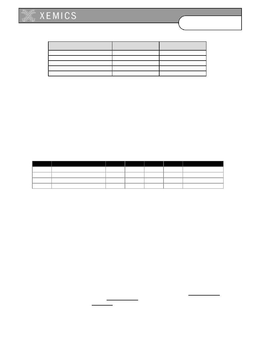
12-4
D0304-40
Datasheet
XE88LC05/05A
if x is even, PBDir[x+1, x]
PBPullup[x]
PB[x] selection on
00
1
analog line 0
01
1
analog line 1
10
1
analog line 2
11
1
analog line 3
XX 0
High
impedance
Table 12-9: Selection of the analog lines for PB[x] when x is even and PBAna[x] = 1
Example:
Set the pads PB[2] and PB[3] on the analog line 3. (the values X depend on the configuration
of others pads)
-
apply high impedance in the analog mode (move RegPBPullup,#0bXXXX00XX)
-
go to analog mode (move RegPBAna,#0bXXXXXX1X)
-
select the analog line3 (move RegPBDir,#0bXXXX11XX and move
RegPBOut,#0bXXXX11XX)
-
connect the analog line to the pins (move RegPBPullup,#0bXXXX11XX)
12.5.2
Port B analog function specification
The table below defines the on-resistance of the switches between the pin and the analog bus for
different conditions. The series resistance between 2 pins of Port B connected to the same analog
line is twice the resistance given in the table.
sym
description
min
typ
max
unit
Comments
Ron
switch resistance
11
k
Note 1
Ron switch
resistance
15
k
Note 2
Cin
input capacitance (off)
3.5
pF
Note 3
Cin
input capacitance (on)
4.5
pF
Note 4
Table 12-10. Analog input specifications.
Note 1: This is the series resistance between the pad and the analog line in 2 cases
1.
VBAT
2.4V and the VMULT peripheral is present on the circuit and enabled.
2.
VBAT
3.0V and the VMULT peripheral is not present on the circuit.
Note 2: This is the series resistance in case VBAT
2.8V and the peripheral VMULT is not present
on the circuit.
Note 3: This is the input capacitance seen on the pin when the pin is not connected to an analog line.
This value is indicative only since it is product and package dependent.
Note 4: This is the input capacitance seen on the pin when the pin is connected to an analog line and
no other pin is connected to the same analog line. This value is indicative only since it is product and
package dependent.
12.6 Port B function capability
The Port B can be used for different functions implemented by other peripherals. The description
below is applicable only in so far the circuit contains these peripherals.
When the counters are used to implement a PWM function (see the documentation of the counters),
the PB[0] and PB[1] terminals are used as outputs (PB[0] is used if CntPWM0 in RegCntConfig1 is
set to 1, PB[1] is used if CntPWM1 in RegCntConfig1 is set to 1) and the PWM generated values
overwrite the values written in RegPBout. However, PBDir(0) and PBDir(1) are not automatically
overwritten and have to be set to 1.

12-5
D0304-40
Datasheet
XE88LC05/05A
If OutputCkXtal is set in RegSysMisc, the Xtal clock is output on PB[3] (EnableXtal in RegSysClock
must be set to 1). This overrides the value contained in PBOut(3). However, PBDir(3) must be set to
1. The duty cycle of the clock signal is about 50%.
Similarly, if OutputCkCpu is set in RegSysMisc, the CPU frequency is output on PB[2]. This
overrides the value contained in PBOut(2). However, PBDir(2) must be set to 1.
The frequency of the CPU clock depends on the selection of the CpuSel bit in the RegSysClock
register (see clock_gen_ff).
Pins PB[5] and PB[4] can be used for S1 and S0 of the USRT (see USRT documentation) when the
UsrtEnable bit is set in RegUsrtCtrl. The PB[5] and PB[4] then become open-drain. This overrides
the values contained in PBOpen(5:4), PBOut(5:4) and PBDir(5:4). If there is no external pull-up
resistor on these pins, internal pull-ups should be selected by setting PBPullup(5:4). When S0 is an
output, the pin PB[4] takes the value of UsrtS0 in RegUrstS0. When S1 is an output, the pin PB[5]
takes the value of UsrtS1 in RegUrstS1.
Pins PB[6] and PB[7] can be used by the UART (see UART documentation). When UartEnTx in
RegUartCtrl is set to 1, PB[6] is used as output signal Tx. When UartEnRx in RegUartCtrl is set to 1,
PB[7] is used as input signal Rx. This overrides the values contained in PBOut(7:6) and PBDir(7:6).
12.7 Port B digital capabilities
12.7.1
Port B digital configuration
The direction of each bit within Port B (input only or input/output) can be individually set using the
RegPBDir register. If PBDir[x] = 1, both the input and output buffer are active on the corresponding
Port B. If PBDir[x] = 0, the corresponding Port B pin is an input only and the output buffer is in high
impedance. After reset (resetpconf) Port B is in input only mode (PBDir[x] are reset to 0).
The input values of Port B are available in RegPBIn (read only). Reading is always direct - there is no
debounce function in Port B. In case of possible noise on input signals, a software debouncer with
polling or an external hardware filter have to be realized. The input buffer is also active when the port
is defined as output and allows to read back the effective value on the pin.
Data stored in RegPBOut are output at Port B if PBDir[x] is 1. The default value after reset is low (0).
When a pin is in output mode (PBDir[x] is set to 1), the output can be a conventional CMOS (Push-
Pull) or a N-channel Open-drain, driving the output only low. By default, after reset (resetpconf) the
PBOpen[x] in RegPBOpen is cleared to 0 (push-pull). If PBOpen[x] in RegPBOpen is set to 1 then
the internal P transistor in the output buffer is electrically removed and the output can only be driven
low (PBOut[x]=0). When PBOut[x]=1, the pin is high Impedance. The internal pull-up or an external
pull-up resistor can be used to drive the pin high.
Note: Because the P transistor actually exists (this is not a real Open-drain output) the pull-up range
is limited to VDD + 0.2V (avoid forward bias the P transistor / diode).
Each bit can be set individually for pull-up or not using register RegPBPullup. Input is pulled up when
its corresponding bit in this register is set to 1. Default status after (resetpconf) is 0, which means
without pull up. To limit power consumption, pull-up resistors are only enabled when the associated
pin is either a digital input or an N-channel open-drain output with the pad set to 1. In the other cases
(push-pull output or open-drain output driven low), the pull up resistors are disabled independent of
the value in RegPBPullup.
After power-on reset, the Port B is configured as an input port without pull-up.

12-6
D0304-40
Datasheet
XE88LC05/05A
The input buffer is always active, except in analog mode. This means that the Port B input should be a
valid digital value at all times unless the pin is set in analog mode. Violating this rule may lead to
higher power consumption.
12.7.2
Port B digital function specification
Sym
description
min
typ
max
unit Comments
V
INH
Input high voltage
0.7*VBAT
VBAT
V
VBAT
2.4V
V
INL
Input low voltage
VSS
0.2*VBAT
V
VBAT
2.4V
V
OH
Output high voltage
VBAT-0.4
VBAT V
VBAT=1.2V,
I
OH
=0.3mA
VBAT=2.4V, I
OH
=5.0mA
VBAT=4.5V, I
OH
=8.0mA
V
OL
Output low voltage
VSS
VSS+0.4 V VBAT=1.2V,
I
OL
=0.3mA
VBAT=2.4V, I
OL
=12.0mA
VBAT=4.5V, I
OL
=15.0mA
R
PU
Pull-up resistance
20
50
80
k
Cin
Input capacitance
3.5
pF
Note 1
Note 1: this value is indicative only since it depends on the package.

13-1
pc_ff - 1.0 ≠ 29 august 2002
D0304-40
Datasheet
XE88LC05/05A
13 Port C
13.1
Features
13-2
13.2
Overview
13-2
13.3
Port C (PC) Operation
13-2
13.4
Register map
13-2
13.5
Port C electrical specification
13-3

13-2
D0304-40
Datasheet
XE88LC05/05A
13.1 Features
∑
Input / output port, 8 bits wide
∑
Each bit can be set individually for input or output
13.2 Overview
Port C (PC) is a general purpose 8 bit input/output digital port.
Figure 13-1 shows its structure.
Figure 13-1: structure of Port C
13.3 Port C (PC) Operation
The direction of each bit within Port C (input or output) can be individually set by using the RegPCDir
register. If PCDir[x] = 1, the corresponding Port C pin becomes an output. After reset, Port C is in
input mode (PCDir[x] are reset to 0).
Output mode:
Data is stored in RegPCOut prior to output at Port C.
Input mode:
The status of Port C is available in RegPCIn (read only). Reading is always direct - there is no digital
debounce function associated with Port C. In case of possible noise on input signals, a software
debouncer or an external filter must be realized.
By default after reset, Port C is configured as an input port.
13.4 Register map
There are three registers in the Port C (PC), namely RegPCIn, RegPCOut and RegPCDir. Table
13-1 to Table 13-3 show the mapping of control bits and functionality of these registers.
Pos.
RegPCIn
Rw
Reset
Description
7-0
PCIn
r
-
pad PC input value
Table 13-1. RegPCIn
RegPCIn
RegPCOut
RegPCDir
8
8
8
Port C
13-3
D0304-40
Datasheet
XE88LC05/05A
Pos.
RegPCOut
Rw
Reset
Description
7-0
PCOut
r w
0 resetpconf
pad PC output value
Table 13-2. RegPCOut
Pos.
RegPCDir
Rw
Reset
Description
7-0
PCDir
r w
0 resetpconf
pad PC direction (0=input)
Table 13-3. RegPCDir
13.5 Port C electrical specification
Sym
description
min
typ
max
unit Comments
V
INH
Input high voltage
0.7*VBAT
VBAT
V
VBAT
2.4V
V
INL
Input low voltage
VSS
0.2*VBAT
V
VBAT
2.4V
V
OH
Output high voltage
VBAT-0.4
VBAT V
VBAT=1.2V,
I
OH
=0.3mA
VBAT=2.4V, I
OH
=5.0mA
VBAT=4.5V, I
OH
=8.0mA
V
OL
Output low voltage
VSS
VSS+0.4 V VBAT=1.2V,
I
OL
=0.3mA
VBAT=2.4V, I
OL
=12.0mA
VBAT=4.5V, I
OL
=15.0mA
Cin
Input capacitance
3.0
pF
Note 1
Note 1: this value is indicative only since it depends on the package.
Table 13-4. Port C electrical specification

14-1
uart_ff - 1.0 ≠ 05 september 2002
D0304-40
Datasheet
XE88LC05/05A
14 UART
14.1
Features
14-2
14.2
Overview
14-2
14.3
Registers map
14-2
14.4
Interrupts map
14-3
14.5
Uart baud rate selection
14-3
14.5.1
Uart on the RC oscillator
14-3
14.5.2
Uart on the crystal oscillator
14-4
14.6
Function description
14-4
14.6.1
Configuration bits
14-4
14.6.2
Transmission 14-5
14.6.3
Reception
14-6
14.7
Interrupt or polling
14-6
14.8
Software hints
14-7
14-2
D0304-40
Datasheet
XE88LC05/05A
14.1 Features
∑
Full duplex operation with buffered receiver and transmitter.
∑
Internal baud rate generator with 12 programmable baud rates (300 - 115200).
∑
7 or 8 bits word length.
∑
Even, odd, or no-parity bit generation and detection
∑
1 stop bit
∑
Error receive detection: Start, Parity, Frame and Overrun
∑
Receiver echo mode
∑
2 interrupts (receive full and transmit empty)
∑
Enable receive and/or transmit
∑
Invert pad Rx and/or Tx
14.2 Overview
The UART pins are PB[7], which is used as Rx - receive and PB[6] as Tx - transmit.
14.3 Registers
map
pos.
RegUartCmd
rw
Reset
Description
7
SelXtal
rw
0 resetsystem
Select input clock: 0 = RC/external, 1 = xtal
6
UartEnRx2
rw
0 resetsystem
Enable Uart Reception
5-3
UartRcSel(2:0)
rw
000 resetsystem
RC prescaler selection
2
UartPM
rw
0 resetsystem
Select parity mode: 0 = odd, 1 = even
1
UartPE
rw
0 resetsystem
Enable parity: 1 = with parity, 0 = no parity
0
UartWL
rw
1 resetsystem
Select word length: 1 = 8 bits, 0 = 7 bits
Table 14-1: RegUartCmd
Pos.
RegUartCtrl
rw
reset
Description
7
UartEcho
rw
0 resetsystem
Enable echo mode:
1 = echo Rx->Tx, 0 = no echo
6
UartEnRx1
rw
0 resetsystem
Enable uart reception
5
UartEnTx
rw
0 resetsystem
Enable uart transmission
4
UartXRx
rw
0 resetsystem
Invert pad Rx
3
UartXTx
rw
0 resetsystem
Invert pad Tx
2-0
UartBR(2:0)
rw
101 resetsystem
Select baud rate
Table 14-2: RegUartCtrl
pos.
RegUartTx
rw
reset
Description
7-0 UartTx rw 00000000
resetsystem
Data to be sent
Table 14-3: RegUartTx
14-3
D0304-40
Datasheet
XE88LC05/05A
pos.
RegUartTxSta
rw
reset
description
7-2 - r 000000
Unused
1
UartTxBusy
r
0 resetsystem
Uart busy transmitting
0 UartTxFull r 0
resetsystem
RegUartTx full
Set by writing to RegUartTx
Cleared when transferring RegUartTx into
internal shift register
Table 14-4: RegUartTxSta
pos.
RegUartRx
rw
reset
description
7-0 UartRx r 00000000
resetsystem
Received data
Table 14-5: RegUartRx
pos.
RegUartRxSta
rw
Reset
description
7-6 - r 00
Unused
5
UartRxSErr
r
0 resetsystem
Start error
4
UartRxPErr
r
0 resetsystem
Parity error
3
UartRxFErr
r
0 resetsystem
Frame error
2
UartRxOErr
rc
0 resetsystem
Overrun error
Cleared by writing RegUartRxSta
1
UartRxBusy
r
0 resetsystem
Uart busy receiving
0 UartRxFull r 0
resetsystem
RegUartRx full
Cleared by reading RegUartRx
Table 14-6: RegUartRxSta
14.4 Interrupts
map
interrupt source
default mapping in the interrupt manager
Irq_uart_Tx
IrqHig(1)
Irq_uart_Rx
IrqHig(0)
Table 14-7: Interrupts map
14.5 Uart baud rate selection
In order to have correct baud rates, the Uart interface has to be fed with a stable and trimmed clock
source. The clock source can be the RC oscillator or the crystal oscillator. The precision of the baud
rate will depend on the precision of the selected clock source.
14.5.1
Uart on the RC oscillator
To select the RC oscillator for the Uart, the bit SelXtal in RegUartCmd has to be 0.
In order to obtain a correct baud rate, the RC oscillator frequency has to be set to one of the
frequencies given in the table on the next page. The precision of the obtained baud rate is directly
proportional to the frequency deviation with respect to the values in the table.
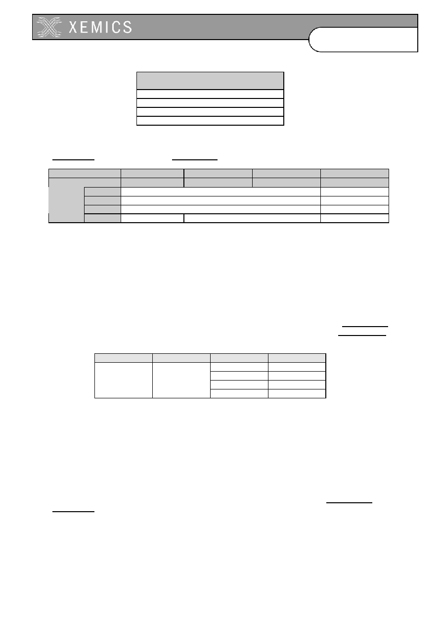
14-4
D0304-40
Datasheet
XE88LC05/05A
Frequency selection for correct Uart
baud rate with RC oscillator (Hz)
2'457'600
1'843'200
1'228'800
614'400
For each of these frequencies, the baud rate can be selected with the bits UartBR(2:0) in
RegUartCtrl and UartRcSel(2:0) in RegUartCmd as shown in Table 14-8
RC frequency (Hz)
2'457'600
1'228'800
614'400
1'843'200
UartRcSel
010
001
000
000
111 38400
115200
110 19200
57600
101 9600
28800
UartBR
100 Not
possible
4800
14400
Table 14-8: Uart baud rate with RC clock
Note: The precision of the baud rate is directly proportional to the frequency deviation of the used
clock from the ideal frequency given in the table. In order to increase the precision and stability of the
RC oscillator, the DFLL (digital frequency locked loop) can be used with the crystal oscillator as a
reference.
14.5.2
Uart on the crystal oscillator
In order to use the crystal oscillator as the clock source for the Uart, the bit SelXtal in RegUartCmd
has to be set. The crystal oscillator has to be enabled by setting the EnableXtal bit in RegSysClock.
The baud rate selection is done using the UartBR and UartRcSel bits as shown in Table 14-9.
Xtal freq. (Hz)
UartRcSel
UartBR
Baud rate
011 2400
010 1200
001 600
32768 001
000 300
Table 14-9: Uart baud rate with Xtal clock
Due to the odd ratio between the crystal oscillator frequency and the baud rate, the generated baud
rate has a systematic error of ≠2.48%.
14.6 Function
description
14.6.1 Configuration
bits
The configuration bits of the Uart serial interface can be found in the registers RegUartCmd and
RegUartCtrl.
The bit SelXtal is used to select the clock source (see chapter 14.5). The bits UartSelRc and UartBR
select the baud rate (see chapter 14.5).
The bits UartEnTx is used to enable or disable the transmission.

14-5
D0304-40
Datasheet
XE88LC05/05A
The bits UartEnRx1 and UartEnRx2 are used to enable or disable the reception. When one is set to
1, the reception is enabled.
The word length (7 or 8 data bits) can be chosen with UartWL. A parity bit is added during
transmission or checked during reception if UartPE is set. The parity mode (odd or even) can be
chosen with UartPM.
Setting the bits UartXRx and UartXTx inverts the Rx respectively Tx signals.
The bit UartEcho is used to send the received data automatically back. The transmission function
becomes then: Tx = Rx XOR UartXTx.
14.6.2 Transmission
In order to send data, the transmitter has to be enabled by setting the bit UartEnTx. Data to be sent
has to be written to the register RegUartTx. The bit UartTxFull in RegUartTxSta then goes to 1,
indicating to the transmitter that a new word is available. As soon as the transmitter has finished
sending the previous word, it then loads the contents of the register RegUartTx to an internal shift
register and clears the UartTxFull bit. An interrupt is generated on Irq_uart_Tx at the falling edge of
the UartTxFull bit. The bit UartTxBusy in RegUartTxSta shows that the transmitter is busy
transmitting a word.
A timing diagram is shown in Figure 14-1. Data are first sent LSB.
New data should be written to the register RegUartTx only while UartTxFull is 0, otherwise data will
be lost.
Asynchronous Transmission
write to RegUartTx
RegUartTx
word 1
reguarttx_shift
word 1
shift clock
Tx
start
b0
b1
b6/7
parity
stop
UartTxBusy
UartTxFull
Irq_uart_Tx
Asynchronous Transmission (back to back)
word 1
word 2
write to RegUartTx
RegUartTx
word 1
word 2
reguarttx_shift
word 1
word 2
shift clock
Tx
start
b0
b6/7
stop
start
UartTxBusy
UartTxFull
Irq_uart_Tx
Figure 14-1. Uart transmission timing diagram.

14-6
D0304-40
Datasheet
XE88LC05/05A
14.6.3 Reception
On detection of the start bit, the UartRxBusy bit is set. On detection of the stop bit, the received data
are transferred from the internal shift register to the register RegUartRx. At the same time, the
UartRxFull bit is set and an interrupt is generated on Irq_uart_Rx. This indicates that new data is
available in RegUartRx. The timing diagram is shown in Figure 14-2.
The UartRxFull bit is cleared when RegUartRx is read. If the register was not read before the
receiver transfers a new word to it, the bit UartRxOErr (overflow error) is set and the previous
contents of the register is lost. UartRxOErr is cleared by writing any data to RegUartRxSta.
The bit UartRxSErr is set if a start error has been detected. The bit is updated at data transfer to
RegUartRx.
The bit UartRxPErr is set if a parity error has been detected, i.e. the received parity bit is not equal to
the calculated parity of the received data. The bit is updated at data transfer to RegUartRx.
The bit UartRxFErr in RegUartRxSta shows that a frame error has been detected. No stop bit has
been detected.
Asynchronous Reception
read of RegUartRx (software)
reguartrx_shift
word 1
RegUartRx
word 1
shift clock
Rx
start
b0
b6/7
parity
stop
UartRxBusy
UartRxFull
Irq_uart_Rx
Figure 14-2. Uart reception timing diagram.
14.7 Interrupt or polling
The transmission and reception software can be driven by interruption or by polling the status bits.
Interrupt driven reception: each time an Irq_uart_Rx interrupt is generated, a new word is available in
RegUartRx. The register has to be read before a new word is received.
Interrupt driven transmission: each time the contents of RegUartTx is transferred to the transmission
shift register, an Irq_uart_Tx interrupt is generated. A new word can then be written to RegUartTx.
Reception driven by polling: the UartRxFull bit is to be read and checked. When it is 1, the
RegUartRx register contains new data and has to be read before a new word is received.
Transmission driven by polling: the UartTxFull bit is to read and checked. When it is 0, the
RegUartTx register is empty and a new word can be written to it.

14-7
D0304-40
Datasheet
XE88LC05/05A
14.8 Software
hints
Example of program for a transmission with polling:
1. The RegUartCmd register and the RegUartCtrl register are initialized (for example: 8 bit word
length, odd parity, 9600 baud, enable Uart transmission).
2. Write a byte to RegUartTx.
3. Wait until the UartTxFull bit in RegUartTxSta register equals 0.
4. Jump to 2 to write the next byte if the message is not finished.
5. End of transmission.
Example of program for a transmission with interrupt:
1. The RegUartCmd register and the RegUartCtrl register are initialized (for example: 8 bit word
length, odd parity, 9600 baud, enable Uart transmission).
2. Write a byte to RegUartTx.
3. After an interrupt and if the message is not finished, jump to 2
4. End of transmission.
Example of program for a reception with polling:
1. The
RegUartCmd register and the RegUartCtrl register are initialized (for example: 8 bit word
length, odd parity, 9600 baud, enable Uart reception).
2. Wait until the UartRxFull bit in the RegUartRxSta register equals 1.
3. Read the RegUartRxSta and check if there is no error.
4. Read data in RegUartRx.
5. If data is not equal to End-Of-Line, then jump to 2.
6. End of reception.
Example of program for a reception with interrupt:
1. The RegUartCmd register and the RegUartCtrl register are initialized (for example: 8 bit word
length, odd parity, 9600 baud, enable Uart reception).
2. When there is an interrupt, jump to 3
3. Read RegUartRxSta and check if there is no error.
4. Read data in RegUartRx.
5. If data is not equal to End-Of-Line, then jump to 2.
6. End of reception.

15-1
usrt_ff - 1.1 ≠ 30 september 2002
D0304-40
Datasheet
XE88LC05/05A
15 USRT
15.1
Features
15-2
15.2
Overview
15-2
15.3
Register map
15-2
15.4
Interrupts map
15-4
15.5
Conditional edge detection 1
15-4
15.6
Conditional edge detection 2
15-4
15.7
Interrupts or polling
15-5
15.8
Function description
15-5
15-2
D0304-40
Datasheet
XE88LC05/05A
15.1 Features
The USRT implements a hardware support for software implemented serial protocols:
∑
Control of two external lines S0 and S1 (read/write).
∑
Conditional edge detection generates interrupts.
∑
S0 rising edge detection.
∑
S1 value is stored on S0 rising edge.
∑
S0 signal can be forced to 0 after a falling edge on S0 for clock stretching in the low state.
∑
S0 signal can be stretched in the low state after a falling edge on S0 and after a S1 conditional
detection.
15.2 Overview
The USRT block supports software universal synchronous receiver and transmitter mode interfaces.
External lines S0 and S1 respectively correspond to clock line and data line. S0 is mapped to PB[4]
and S1 to PB[5] when the USRT block is enabled. It is independent from RegPBdir (Port B can be
input or output). When USRT is enabled, the configurations in port B for PB[4] and PB[5] are
overwritten by the USRT configuration. Internal pull-ups can be used by setting the PBPullup[5:4]
bits.
Conditional edge detections are provided.
RegUsrtS1 can be used to read the S1 data line from PB[5] in receive mode or to drive the output S1
line PB[5] by writing it when in transmit mode. It is advised to read S1 data when in receive mode from
the RegUsrtBufferS1 register, which is the S1 value sampled on a rising edge of S0.
15.3 Register map
Block configuration registers:
pos.
RegUsrtS1
rw
reset
function
7-1 -
r 0000000
Unused
0
UsrtS1
rw
1 resetsystem
Write: data S1 written to pad PB[5]),
Read: value on PB[5] (not UsrtS1 value).
Table 15-1: RegUsrtS1
pos.
RegUsrtS0
rw
Reset
function
7-1 -
r 0000000
Unused
0
UsrtS0
rw
1 resetsystem
Write: clock S0 written to pad PB[4],
Read: value on PB[4] (not UsrtS0 value).
Table 15-2: RegUsrtS0
The values that are read in the registers RegUsrtS1 and RegUsrtS0 are not necessarily the same as
the values that were written in the register. The read value is read back on the circuit pins, not in the
registers. Since the outputs are open drain, a value different from the register value may be forced by
an external circuit on the circuit pins.

15-3
D0304-40
Datasheet
XE88LC05/05A
pos.
RegUsrtCtrl
rw
reset
function
7-4 -
r "0000"
Unused
3
UsrtWaitS0
r
0 resetsystem
Clock stretching flag (0=no stretching),
cleared by writing RegUsrtBufferS1
2 UsrtEnWaitCond1
rw
0
resetsystem
Enable stretching on UsrtCond1 detection
(0=disable)
1
UsrtEnWaitS0
rw
0 resetsystem
Enable stretching operation (0=disable)
0 UsrtEnable
rw
0
resetsystem
Enable USRT operation (0=disable)
Table 15-3: RegUsrtCtrl
pos.
RegUsrtCond1
rw
reset
function
7-1 -
r 0000000
Unused
0 UsrtCond1
r/c
0
resetsystem
State
of condition 1 detection (1 =detected),
cleared when written.
Table 15-4: RegUsrtCond1
pos.
RegUsrtCond2
rw
reset
function
7-1 -
r 0000000
Unused
0 UsrtCond2
r/c
0
resetsystem
State
of condition 2 detection (1 =detected),
cleared when written.
Table 15-5: RegUsrtCond2
pos. RegUsrtBufferS1
rw
reset
function
7-1 -
r 0000000
Unused
r
Value on S1 at last S0 rising edge.
Clear RegUsrtEdgeS0 bit in RegUsrtEdgeS0
0 UsrtBufferS1
w
x
Clear UsrtWaitS0 bit in RegUsrtCtrl with any
value
Table 15-6: RegUsrtBufferS1
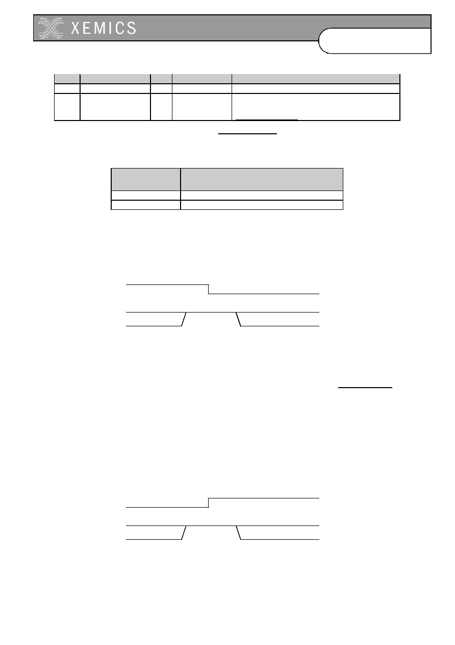
15-4
D0304-40
Datasheet
XE88LC05/05A
pos.
RegUsrtEdgeS0
rw
reset
function
7-1 -
r 0000000
Unused
0 UsrtEdgeS0 r 0
resetsystem
State of rising edge detection on S0
(1=detected). Cleared by reading
RegUsrtBufferS1
Table 15-7: RegUsrtEdgeS0
15.4 Interrupts map
interrupt
source
default mapping in the interrupt manager
Irq_cond1 RegIrqMid(7)
Irq_cond2 RegIrqMid(6)
Table 15-8: Interrupts map
15.5 Conditional edge detection 1
S1
S0
Figure 15-1: Condition 1
Condition 1 is satisfied when S0=1 at the falling edge of S1. The bit UsrtCond1 in RegUsrtCond1 is
set when the condition 1 is detected and the USRT interface is enabled (UsrtEnable=1). Condition 1
is asserted for both modes (receiver and transmitter). The UsrtCond1 bit is read only and is cleared
by all reset conditions and by writing any data to its address.
Condition 1 occurrence also generates an interrupt on Irq_cond1.
15.6 Conditional edge detection 2
S1
S0
Figure 15-2: Condition 2

15-5
D0304-40
Datasheet
XE88LC05/05A
Condition 2 is satisfied when S0=1 at the rising edge of S1. The bit UsrtCond2 in RegUsrtCond2 is
set when the condition 2 is detected and the USRT interface is enabled. Condition 2 is asserted for
both modes (receiver and transmitter). The UsrtCond2 bit is read only and is cleared by all reset
conditions and by writing any data to its address.
Condition 2 occurrence also generates an interrupt on Irq_cond2.
15.7 Interrupts or polling
In receive mode, there are two possibilities for detecting condition 1 or 2: the detection of the condition
can generate an interrupt or the registers can be polled (reading and checking the RegUsrtCond1
and RegUsrtCond2 registers for the status of USRT communication).
15.8 Function description
The bit UsrtEnable in RegUsrtCtrl is used to enable the USRT interface and controls the PB[4] and
PB[5] pins. This bit puts these two port B lines in the open drain configuration requested to use the
USRT interface.
If no external pull-ups are added on PB[4] and PB[5], the user can activate internal pull-ups by setting
PBPullup[4] and PBPullup[5] in RegPBPullup.
The bits UsrtEnWaitS0, UsrtEnWaitCond1, UsrtWaitS0 in RegUsrtCtrl are used for
transmitter/receiver control of USRT interface.
Figure 15-3 shows the unconditional clock stretching function which is enabled by setting
UsrtEnWaitS0.
S0
UsrtWaitS0
write Reg UsrtBufferS1
Figure 15-3: S0 Stretching (UsrtEnWaitS0=1)
When UsrtEnWaitS0 is 1, the S0 line will be maintained at 0 after its falling edge (clock stretching).
UsrtWaitS0 is then set to 1, indicating that the S0 line is forced low. One can release S0 by writing to
the RegUsrtBufferS1 register.
The same can be done in combination with condition 1 detection by setting the UsrtEnWaitCond1 bit.
Figure 15-4 shows the conditional clock stretching function which is enabled by setting
UsrtEnWaitCond1.

15-6
D0304-40
Datasheet
XE88LC05/05A
S0
UsrtWaitS0
write Reg UsrtBufferS1
S1
Figure 15-4: Conditional stretching (UsrtEnWaitCond1=1)
When UsrtEnWaitCond1 is 1, the S0 signal will be stretched in its low state after its falling edge if the
condition 1 has been detected before (UsrtCond1=1). UsrtWaitS0 is then set to 1, indicating that the
S0 line is forced low. One can release S0 by writing to the RegUsrtBufferS1 register.
Figure 15-5 shows the sampling function implemented by the UsrtBufferS1 bit. The bit UsrtBufferS1
in RegUsrtBufferS1 is the value of S1 sampled on PB[4] at the last rising edge of S0. The bit
UsrtEdgeS0 in RegUsrtEdgeS0 is set to one on the same S0 rising edge and is cleared by a read
operation of the RegUsrtBufferS1 register. The bit therefore indicates that a new value is present in
the RegUsrtBufferS1 which has not yet been read.
S0
UsrtBufferS1
read Reg UsrtBufferS1
S1
UsrtEdgeS0
Figure 15-5: S1 sampling

16-1
Acquisition chain ≠ 2.5 ≠ 30 Avril 2002
D0304-40
Datasheet
XE88LC05/05A
16. Acquisition
chain
16.1 ZoomingADC
Features............................................................................................... 16-2
16.2 Overview ......................................................................................................................... 16-2
16.3 Register
map .................................................................................................................. 16-2
16.4 ZoomingADC
Description .......................................................................................... 16-4
16.4.1 Acquisition Chain ............................................................................................................. 16-4
16.4.2 Peripheral Registers ........................................................................................................ 16-6
16.4.3 Continuous-Time vs. On-Request ................................................................................... 16-8
16.5 Input
Multiplexers .......................................................................................................... 16-9
16.6 Programmable
Gain Amplifiers .................................................................................. 16-10
16.6.1 PGA & ADC Enabling .................................................................................................... 16-12
16.6.2 PGA1 ............................................................................................................................. 16-12
16.6.3 PGA2 ............................................................................................................................. 16-12
16.6.4 PGA3 ............................................................................................................................. 16-12
16.7 ADC
Characteristics .................................................................................................... 16-13
16.7.1 Conversion Sequence ................................................................................................... 16-13
16.7.2 Sampling Frequency...................................................................................................... 16-14
16.7.3 Over-Sampling Ratio ..................................................................................................... 16-14
16.7.4 Elementary
Conversions................................................................................................ 16-14
16.7.5 Resolution ...................................................................................................................... 16-15
16.7.6 Conversion
Time & Throughput..................................................................................... 16-16
16.7.7 Output
Code Format ...................................................................................................... 16-16
16.7.8 Power
Saving Modes..................................................................................................... 16-18
16.8 Specifications
and
Measured Curves........................................................................ 16-18
16.8.1 Default Settings ............................................................................................................. 16-19
16.8.2 Specifications................................................................................................................. 16-20
16.8.3 Linearity ......................................................................................................................... 16-22
16.8.3.1 Integral non-linearity ...................................................................................................... 16-22
16.8.3.2 Differential non-linearity ................................................................................................. 16-25
16.8.4 Noise.............................................................................................................................. 16-26
16.8.5 Gain Error and Offset Error............................................................................................ 16-27
16.8.6 Power
Consumption ...................................................................................................... 16-28
16.8.7 Power Supply Rejection Ratio ....................................................................................... 16-30
16.9 Application Hints ......................................................................................................... 16-31
16.9.1 Input
Impedance ............................................................................................................ 16-31
16.9.2 PGA Settling or Input Channel Modifications ................................................................ 16-31
16.9.3 PGA Gain & Offset, Linearity and Noise........................................................................ 16-31
16.9.4 Frequency
Response..................................................................................................... 16-32
16.9.5 Power
Reduction ........................................................................................................... 16-33
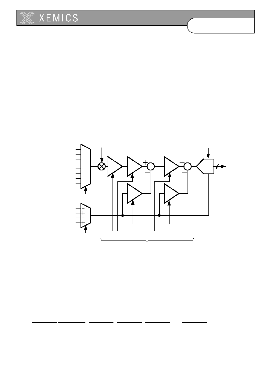
16-2
D0304-40
Datasheet
XE88LC05/05A
16.1 ZoomingADC
Features
The ZoomingADC
is a complete and versatile low-power analog front-end interface typically
intended for sensing applications. The key features of the ZoomingADC
are:
Programmable 6 to 16-bit dynamic range oversampled ADC
∑
Flexible gain programming between 0.5 and 1000
∑
Flexible and large range offset compensation
∑
4-channel differential or 8-channel single-ended input multiplexer
∑
2-channel differential reference inputs
∑
Power saving modes
∑
Direct interfacing to CoolRisc
microcontroller
16.2 Overview
PGA1
PGA2
PGA3
ADC
MU
X
MU
X
GD1
GD2
GD3
OFF2
OFF3
0
1
2
3
4
5
6
7
0
1
2
3
Analog
Inputs
16
V
IN
f
S
V
REF
V
IN,ADC
Gain1 Gain2
Gain3
Offset3
Offset2
Reference
Selection
Input
Selection
ZOOM
Reference
Inputs
V
D1
V
D2
f
S
Figure 16-1. ZoomingADC
general functional block diagram
The total acquisition chain consists of an input multiplexer, 3 programmable gain amplifier stages and
an oversampled A/D converter. The reference voltage can be selected on two different channels. Two
offset compensation amplifiers allow for a wide offset compensation range. The programmable gain
and offset allow one to zoom in on a small portion of the reference voltage defined input range.
16.3 Register
map
There are eight registers in the acquisition chain (AC), namely RegAcOutLsb, RegAcOutMsb,
RegAcCfg0, RegAcCfg1, RegAcCfg2, RegAcCfg3, RegAcCfg4 and RegAcCfg5. Table 16-2 to
Table 16-9 show the mapping of control bits and functionality of these registers while Table 16-1 gives
an overview of these eight.
16-3
D0304-40
Datasheet
XE88LC05/05A
The register map only gives a short description of the different configuration bits. More detailed
information is found in subsequent sections.
register name
RegAcOutLsb
RegAcOutMsb
RegAcCfg0
RegAcCfg1
RegAcCfg2
RegAcCfg3
RegAcCfg4
RegAcCfg5
Table 16-1: AC registers
pos.
RegAcOutLsb
rw
reset
description
7:0 Out[7:0]
r
00000000
resetsystem
LSB of the output code
Table 16-2: RegAcOutLsb
pos.
RegAcOutMsb
rw
reset
description
7:0 Out[15:8]
r
00000000
resetsystem
MSB of the output code
Table 16-3: RegAcOutMsb
pos.
RegAcCfg0
rw
reset
description
7
Start
w r0 0 resetsystem
starts a conversion
6:5
SET_NELCONV[1:0]
r w
01 resetsystem
sets the number of elementary conversions
4:2 SET_OSR[2:0]
r
w
010
resetsystem
sets the oversampling rate of an elementary
conversion
1
CONT
r w
0 resetsystem
continuous conversion mode
0 reserved
r
w
0
resetsystem
Table 16-4: RegAcCfg0
pos.
RegAcCfg1
rw
reset
description
7:6 IB_AMP_ADC[1:0]
r
w
11
resetsystem Bias current selection of the ADC converter
5:4 IB_AMP_PGA[1:0]
r
w
11
resetsystem
Bias current selection of the PGA stages
3:0 ENABLE[3:0]
r
w
0000
resetsystem
Enables the different PGA stages and the ADC
Table 16-5: RegAcCfg1
pos.
RegAcCfg2
rw
reset
description
7:6 FIN[1:0]
r
w
00
resetsystem
Sampling frequency selection
5:4 PGA2_GAIN[1:0]
r
w
00
resetsystem
PGA2 stage gain selection
3:0 PGA2_OFFSET[3:0]
r
w
0000
resetsystem
PGA2 stage offset selection
Table 16-6: RegAcCfg2
16-4
D0304-40
Datasheet
XE88LC05/05A
pos.
RegAcCfg3
rw
reset
description
7 PGA1_GAIN
r
w
0
resetsystem
PGA1 stage gain selection
6:0 PGA3_GAIN[6:0] r
w
0000000
resetsystem
PGA3 stage gain selection
Table 16-7: RegAcCfg3
pos.
RegAcCfg4
rw
reset
description
7 reserved
r
0
Unused
6:0 PGA3_OFFSET[6:0]
r
w 0000000
resetsystem
PGA3 stage offset selection
Table 16-8: RegAcCfg4
pos.
RegAcCfg5
rw
reset
description
7
BUSY
r
0 resetsystem
Activity flag
6
DEF
w r0 0
Selects default configuration
5:1 AMUX[4:0]
r
w
00000
resetsystem
Input channel configuration selector
0
VMUX
r w
0 resetsystem
Reference channel selector
Table 16-9: RegAcCfg5
16.4 ZoomingADC
Description
Figure 16-2 gives a more detailed description of the acquisition chain.
16.4.1 Acquisition
Chain
Figure 16-1 shows the general block diagram of the acquisition chain (AC). A control block (not shown
in Figure 16-1) manages all communications with the CoolRisc
microcontroller.
Analog inputs can be selected among eight input channels, while reference input is selected between
two differential channels.
The core of the zooming section is made of three differential programmable amplifiers (PGA). After
selection of a combination of input and reference signals V
IN
and V
REF
, the input voltage is modulated
and amplified through stages 1 to 3. Fine gain programming up to 1'000V/V is possible. In addition,
the last two stages provide programmable offset. Each amplifier can be bypassed if needed.
The output of the PGA stages is directly fed to the analog-to-digital converter (ADC), which converts
the signal V
IN,ADC
into digital.
Like most ADCs intended for instrumentation or sensing applications, the ZoomingADC
is an over-
sampled converter (See Note
1
). The ADC is a so-called incremental converter, with bipolar operation
(the ADC accepts both positive and negative input voltages). In first approximation, the ADC output
result relative to full-scale (FS) delivers the quantity:
1
Note: Over-sampled converters are operated with a sampling frequency f
S
much higher than the input signal's Nyquist rate
(typically f
S
is 20-1'000 times the input signal bandwidth). The sampling frequency to throughput ratio is large (typically 10-500).
These converters include digital decimation filtering. They are mainly used for high resolution, and/or low-to-medium speed
applications.
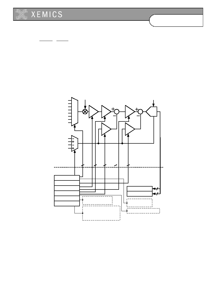
16-5
D0304-40
Datasheet
XE88LC05/05A
2
/
2
/
,
REF
ADC
IN
ADC
V
V
FS
OUT
(Eq. 1)
in two's complement (see Sections 16.4 and 16.7 for details). The output code OUT
ADC
is -FS/2 to
+FS/2 for V
IN,ADC
-V
REF
/2 to +V
REF
/2 respectively. As will be shown in section 16.6, V
IN,ADC
is related
to input voltage V
IN
by the relationship:
REF
TOT
IN
TOT
ADC
IN
V
GDoff
V
GD
V
-
=
,
(V)
(Eq.
2)
where GD
TOT
is the total PGA gain, and GDoff
TOT
is the total PGA offset.
PGA1
PGA2
PGA3
ADC
MU
X
Register Bank
Acquisition Chain
GD1
GD2
GD3
OFF2
OFF3
0
1
2
3
4
5
6
7
0
1
2
3
AC_A
AC_R
RegACOutLSB
RegACOutMSB
8
8
Sampling Frequency f
S
ADC Busy Flag
Default Settings
Conversion Start
Nbr of Elementary Cycles
Over-Sampling Ratio
Continuous vs. On-Request
Power Saving Modes
PGA Enabling
RegACCfg5
RegACCfg4
RegACCfg3
RegACCfg2
RegACCfg1
RegACCfg0
5
2
4
7
7
Inputs
V
IN
f
S
V
REF
V
IN,ADC
f
S
MU
X
Figure 16-2. ZoomingADC
detailed functional block diagram

16-6
D0304-40
Datasheet
XE88LC05/05A
16.4.2 Peripheral
Registers
Figure 16-2 shows a detailed functional diagram of the ZoomingADC
.
In table 16-10 the configuration of the peripheral registers is detailed. The system has a bank of eight
8-bit registers: six registers are used to configure the acquisition chain (
RegAcCfg0 to 5
), and two
registers are used to store the output code of the analog-to-digital conversion (
RegAcOutMsb
&
Lsb
). The register coding of the ADC parameters and performance characteristics are detailed in
Section 16.7.
Table 16-10. Peripheral registers to configure the acquisition chain (AC)
and to store the analog-to-digital conversion (ADC) result
Bit Position
Register
Name
7 6 5 4 3 2 1 0
RegAcOutLsb
OUT[7:0]
RegAcOutMsb
OUT[15:8]
RegAcCfg0
Default values:
START
0
SET_NELC[1:0]
01
SET_OSR[2:0]
010
CONT
0
TEST
0
RegAcCfg1
Default values:
IB_AMP_ADC[1:0]
11
IB_AMP_PGA[1:0]
11
ENABLE[3:0]
0001
RegAcCfg2
Default values:
FIN[1:0]
00
PGA2_GAIN[1:0]
00
PGA2_OFFSET[3:0]
0000
RegAcCfg3
Default values:
PGA1_G
0
PGA3_GAIN[6:0]
0000000
RegAcCfg4
Default values:
0
PGA3_OFFSET[6:0]
0000000
RegAcCfg5
Default values:
BUSY
0
DEF
0
AMUX[4:0]
00000
VMUX
0
With:
∑
OUT
: (r) digital output code of the analog-to-digital converter. (MSB =
OUT[15]
)
∑
START
: (w) setting this bit triggers a single conversion (after the current one is finished). This bit always
reads back 0.
∑
SET_NELC
: (rw) sets the number of elementary conversions to 2
SET_NELC[1:0]
. To compensate for offsets,
the input signal is chopped between elementary conversions (1,2,4,8).
∑
SET_OSR
: (rw) sets the over-sampling rate (OSR) of an elementary conversion to 2
(3+SET_OSR[2:0])
. OSR = 8,
16, 32, ..., 512, 1024.
∑
CONT
: (rw) setting this bit starts a conversion. A new conversion will automatically begin as long as the bit
remains at 1.
∑
TEST
: bit only used for test purposes. In normal mode, this bit is forced to 0 and cannot be overwritten.
∑
IB_AMP_ADC
: (rw) sets the bias current in the ADC to 0.25*(1+
IB_AMP_ADC[1:0]
) of the normal operation
current (25, 50, 75 or 100% of nominal current). To be used for low-power, low-speed operation.
∑
IB_AMP_PGA
: (rw) sets the bias current in the PGAs to 0.25*(1+
IB_AMP_PGA[1:0]
) of the normal
operation current (25, 50, 75 or 100% of nominal current). To be used for low-power, low-speed operation.
∑
ENABLE
: (rw) enables the ADC modulator (bit 0) and the different stages of the PGAs (PGAi by bit i=1,2,3).
PGA stages that are disabled are bypassed.
∑
FIN
: (rw) These bits set the sampling frequency of the acquisition chain. Expressed as a fraction of the
oscillator frequency, the sampling frequency is given as: 00 1/4 f
RC
, 01 1/8 f
RC
, 10 1/32 f
RC
, 11
~8kHz.
∑
PGA1_GAIN
: (rw) sets the gain of the first stage: 0 1, 1 10.
∑
PGA2_GAIN
: (rw) sets the gain of the second stage: 00 1, 01 2, 10 5, 11 10.
∑
PGA3_GAIN
: (rw) sets the gain of the third stage to
PGA3_GAIN[6:0]
1/12.
∑
PGA2_OFFSET
: (rw) sets the offset of the second stage between ≠1 and +1, with increments of 0.2. The MSB
gives the sign (0
positive, 1
negative); amplitude is coded with the bits
PGA2_OFFSET[5:0]
.

16-7
D0304-40
Datasheet
XE88LC05/05A
∑
PGA3_OFFSET
: (rw) sets the offset of the third stage between ≠5.25 and +5.25, with increments of 1/12. The
MSB gives the sign (0
positive, 1
negative); amplitude is coded with the bits
PGA3_OFFSET[5:0]
.
∑
BUSY
: (r) set to 1 if a conversion is running. Note that the flag is set at the effective start of the conversion.
Since the ADC is generally synchronized on a lower frequency clock than the CPU, there might be a small
delay (max. 1 cycle of the ADC sampling frequency) between the writing of the START or CONT bits and the
appearance of BUSY flag.
∑
DEF
: (w) sets all values to their defaults (PGA disabled, max speed, nominal modulator bias current, 2
elementary conversions, over-sampling rate of 32) and starts a new conversion without waiting the end of the
preceding one.
∑
AMUX(4:0):
(rw)
AMUX[4]
sets the mode (0 4 differential inputs, 1 7 inputs with
A(0)
= common
reference)
AMUX(3)
sets the sign (0 straight, 1 cross)
AMUX[2:0]
sets the channel.
∑
VMUX
: (rw) sets the differential reference channel (0
R(1)
and
R(0)
, 1
R(3)
and
R(2)
).
(r = read; w = write; rw = read & write)
16-8
D0304-40
Datasheet
XE88LC05/05A
16.4.3 Continuous-Time
vs.
On-Request
The ADC can be operated in two distinct modes: "continuous-time" and "on-request" modes (selected
using the bit
CONT
).
In "continuous-time" mode, the input signal is repeatedly converted into digital. After a conversion is
finished, a new one is automatically initiated. The new value is then written in the result register, and
the corresponding internal trigger pulse is generated. This operation is sketched in Figure 16-3. The
conversion time in this case is defined as T
CONV
.
Internal Trig
Ouput Code
RegACOut[15:0]
T
CONV
BUSY
IRQ
Figure 16-3. ADC "continuous-time" operation
Figure 16-4. ADC "on-request" operation
In the "on-request" mode, the internal behaviour of the converter is the same as in the "continuous-
time" mode, but the conversion is initiated on user request (with the
START
bit). As shown in Figure
16-4, the conversion time is also T
CONV
. Note that the flag is set at the effective start of the conversion.
Since the ADC is generally synchronized on a lower frequency clock than the CPU, there might be a
small delay (max. 1 cycle of the ADC sampling frequency) between the writing of the START or CONT
bits and the appearance of BUSY flag.
Internal Trig
Ouput Code
RegACOut[15:0]
T
CONV
Request
START
BUSY
IRQ

16-9
D0304-40
Datasheet
XE88LC05/05A
16.5 Input
Multiplexers
The ZoomingADC
has eight analog inputs
AC_A(0)
to
AC_A(7)
and four reference inputs
AC_R(0)
to
AC_R(3)
. Let us first define the differential input voltage V
IN
and reference voltage V
REF
respectively as:
INN
INP
IN
V
V
V
-
=
(V)
(Eq. 3)
and:
REFN
REFP
REF
V
V
V
-
=
(V)
(Eq.
4)
As shown in Table 16-11 the inputs can be configured in two ways: either as 4 differential channels
(V
IN1
=
AC_A(1)
-
AC_A(0)
,..., V
IN4
=
AC_A(7)
-
AC_A(6)
), or
AC_A(0)
can be used as a common
reference, providing 7 signal paths all referred to
AC_A(0)
. The control word for the analog input
selection is
AMUX[4:0]
. Notice that the bit
AMUX[3]
controls the sign of the input voltage.
AMUX[4:0]
(RegAcCfg5[5:1])
V
INP
V
INN
AMUX[4:0]
(RegAcCfg5[5:1])
V
INP
V
INN
00x00
00x01
00x10
00x11
AC_A(1)
AC_A(3)
AC_A(5)
AC_A(7)
AC_A(0)
AC_A(2)
AC_A(4)
AC_A(6)
01x00
01x01
01x10
01x11
AC_A(0)
AC_A(2)
AC_A(4)
AC_A(6)
AC_A(1)
AC_A(3)
AC_A(5)
AC_A(7)
10000
10001
10010
10011
10100
10101
10110
10111
AC_A(0)
AC_A(1)
AC_A(2)
AC_A(3)
AC_A(4)
AC_A(5)
AC_A(6)
AC_A(7)
AC_A(0)
11000
11001
11010
11011
11100
11101
11110
11111
AC_A(0)
AC_A(0)
AC_A(1)
AC_A(2)
AC_A(3)
AC_A(4)
AC_A(5)
AC_A(6)
AC_A(7)
Table 16-11. Analog input selection
Similarly, the reference voltage is chosen among two differential channels (V
REF1
=
AC_R(1)-
AC_R(0)
or V
REF2
=
AC_R(3)-AC_R(2)
) as shown in Table 16-12. The selection bit is
VMUX
. The
reference inputs V
REFP
and V
REFN
(common-mode) can be up to the power supply range.

16-10
D0304-40
Datasheet
XE88LC05/05A
VMUX
(RegAcCfg5[0])
V
REFP
V
REFN
0 AC_R(1)
AC_R(0)
1 AC_R(3)
AC_R(2)
Table 16-12. Analog Reference input selection
16.6 Programmable Gain Amplifiers
As seen in Figure 16-1, the zooming function is implemented with three programmable gain amplifiers
(PGA). These are:
∑
PGA1: coarse gain tuning
∑
PGA2: medium gain and offset tuning
∑
PGA3: fine gain and offset tuning
All gain and offset settings are realized with ratios of capacitors. The user has control over each PGA
activation and gain, as well as the offset of stages 2 and 3. These functions are examined hereafter.
ENABLE[3:0]
Block
xxx0
xxx1
ADC disabled
ADC enabled
xx0x
xx1x
PGA1 disabled
PGA1 enabled
x0xx
x1xx
PGA2 disabled
PGA2 enabled
0xxx
1xxx
PGA3 disabled
PGA3 enabled
Table 16-13. ADC & PGA enabling
PGA1_GAIN
PGA1 Gain
GD
1
(V/V)
0 1
1 10
Table 16-14. PGA1 Gain Settings
PGA2_GAIN[1:0]
PGA2 Gain
GD
2
(V/V)
00 1
01 2
10 5
11 10
Table 16-15. PGA2 gain settings
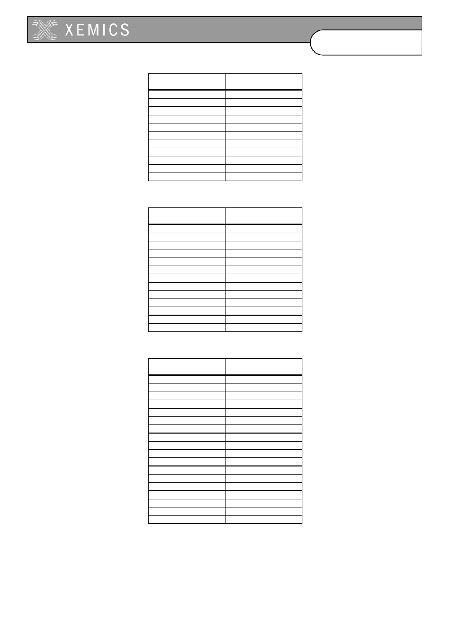
16-11
D0304-40
Datasheet
XE88LC05/05A
PGA2_OFFSET[3:0]
PGA2 Offset
GDoff
2
(V/V)
0000 0
0001 +0.2
0010 +0.4
0011 +0.6
0100 +0.8
0101 +1
1001 -0.2
1010 -0.4
1011 -0.6
1100 -0.8
1101 -1
Table 16-16. PGA2 offset settings
PGA3_GAIN[6:0]
PGA3 Gain
GD
3
(V/V)
0000000 0
0000001 1/12(=0.083)
... ...
0000110 6/12
... ...
0001100 12/12
0010000 16/12
...
0100000 32/12
...
1000000 64/12
...
1111111 127/12(=10.58)
Table 16-17. PGA3 gain settings
PGA3_OFFSET[6:0]
PGA3 Offset
GDoff
3
(V/V)
0000000 0
0000001 +1/12(=+0.083)
0000010 +2/12
... ...
0010000 +16/12
... ...
0100000 +32/12
... ...
0111111 +63/12(=+5.25)
1000000 0
1000001 -1/12(=-0.083)
1000010 -2/12
... ...
1010000 -16/12
... ...
1100000 -32/12
... ...
1111111 -63/12(=-5.25)
Table 16-18. PGA3 offset settings

16-12
D0304-40
Datasheet
XE88LC05/05A
16.6.1
PGA & ADC Enabling
Depending on the application objectives, the user may enable or bypass each PGA stage. This is done
according to the word
ENABLE
and the coding given in Table 16-13. To reduce power dissipation, the
ADC can also be inactivated while idle.
16.6.2 PGA1
The first stage can have a buffer function (unity gain) or provide a gain of 10 (see Table 16-14). The
voltage V
D1
at the output of PGA1 is:
IN
D
V
GD
V
=
1
1
(V)
(Eq. 5)
where GD
1
is the gain of PGA1 (in V/V) controlled with the bit
PGA1_GAIN
.
16.6.3 PGA2
The second PGA has a finer gain and offset tuning capability, as shown in Table 16-15 and Table
16-16. The voltage V
D2
at the output of PGA2 is given by:
REF
D
D
V
GDoff
V
GD
V
-
=
2
1
2
2
(V)
(Eq.
6)
where GD
2
and GDoff
2
are respectively the gain and offset of PGA2 (in V/V). These are controlled
with the words
PGA2_GAIN[1:0]
and
PGA2_OFFSET[3:0]
.
As shown in equation 6, the offset correction is directly proportional to the reference voltage. All drifts
and perturbations on the reference voltage will affect the precision of the offset compensation.
16.6.4 PGA3
The finest gain and offset tuning is performed with the third and last PGA stage, according to the
coding of Table 16-17 and Table 16-18. The output of PGA3 is also the input of the ADC. Thus,
similarly to PGA2, we find that the voltage entering the ADC is given by:
REF
D
ADC
IN
V
GDoff
V
GD
V
-
=
3
2
3
,
(V)
(Eq.
7)
where GD
3
and GDoff
3
are respectively the gain and offset of PGA3 (in V/V). The control words are
PGA3_GAIN[6:0]
and
PGA3_OFFSET[6:0]
. To remain within the signal compliance of the PGA
stages, the condition:
DD
D
D
V
V
V
<
2
1
,
(V)
(Eq. 8)
must be verified.
As shown in equation 7, the offset correction is directly proportional to the reference voltage. All drifts
and perturbations on the reference voltage will affect the precision of the offset compensation.

16-13
D0304-40
Datasheet
XE88LC05/05A
Finally, combining equations Eq. 5 to Eq. 7 for the three PGA stages, the input voltage V
IN,ADC
of the
ADC is related to V
IN
by:
REF
TOT
IN
TOT
ADC
IN
V
GDoff
V
GD
V
-
=
,
(V)
(Eq.
9)
where the total PGA gain is defined as:
1
2
3
GD
GD
GD
GD
TOT
=
(V/V)
(Eq.
10)
and the total PGA offset is:
2
3
3
GDoff
GD
GDoff
GDoff
TOT
+
=
(V/V)
(Eq.
11)
16.7 ADC
Characteristics
The main performance characteristics of the ADC (resolution, conversion time, etc.) are determined
by three programmable parameters:
∑
sampling
frequency
f
S
,
∑
over-sampling
ratio
OSR, and
∑
number of elementary conversions N
ELCONV
.
The setting of these parameters and the resulting performances are described hereafter.
16.7.1 Conversion
Sequence
A conversion is started each time the bit
START
or the bit
DEF
is set. As depicted in Figure 16-5, a
complete analog-to-digital conversion sequence is made of a set of N
ELCONV
elementary incremental
conversions and a final quantization step. Each elementary conversion is made of (OSR+1) sampling
periods T
S
=1/f
S
, i.e.:
S
ELCONV
f
OSR
T
/
)
1
(
+
=
(s)
(Eq.
12)
The result is the mean of the elementary conversion results. An important feature is that the
elementary conversions are alternatively performed with the offset of the internal amplifiers
contributing in one direction and the other to the output code. Thus, converter internal offset is
eliminated if at least two elementary sequences are performed (i.e. if N
ELCONV
2). A few additional
clock cycles are also required to initiate and end the conversion properly.
Conversion index
Offset
T
ELCONV
= (OSR+1)/f
S
Elementary
Conversion
1
+
Elementary
Conversion
2
-
Elementary
Conversion
N
ELCONV
- 1
+
Elementary
Conversion
N
ELCONV
-
Init
End
T
CONV
Conversion
Result
Figure 16-5. Analog-to-digital conversion sequence

16-14
D0304-40
Datasheet
XE88LC05/05A
16.7.2 Sampling
Frequency
The word
FIN[1:0]
is used to select the sampling frequency f
S
(Table 16-19). Three sub-multiples of
the internal RC-based frequency f
RCEXT
can be chosen. For
FIN
= "11", sampling frequency is about
8kHz. Additional information on oscillators and their control can be found in the clock block
documentation.
Sampling Frequency f
S
(Hz)
FIN[1:0]
LC01/05 LC02
00
1/4
f
RC
1/8
f
RCEXT
01
1/8
f
RC
1/16
f
RCEXT
10
1/32
f
RC
1/64
f
RCEXT
11
8kHz
4kHz
Table 16-19. Sampling frequency settings (f
RC
= RC-based frequency)
16.7.3 Over-Sampling
Ratio
The over-sampling ratio (OSR) defines the number of integration cycles per elementary conversion.
Its value is set with the word
SET_OSR[2:0]
in power of 2 steps (see Table 16-20) given by:
0]
:
SET_OSR[2
3
2
+
=
OSR
(-)
(Eq.
13)
SET_OSR[2:0]
(RegAcCfg0[4:2])
Over-Sampling Ratio
OSR (-)
000 8
001 16
010 32
011 64
100 128
101 256
110 512
111 1024
Table 16-20. Over-sampling ratio settings
16.7.4 Elementary
Conversions
As mentioned previously, the whole conversion sequence is made of a set of N
ELCONV
elementary
incremental conversions. This number is set with the word
SET_NELC[1:0]
in power of 2 steps (see
Table 16-21) given by:
0]
:
SET_NELC[1
2
=
ELCONV
N
(-)
(Eq.
14)

16-15
D0304-40
Datasheet
XE88LC05/05A
SET_NELC[1:0]
(RegAcCfg0[6:5])
# of Elementary
Conversions
N
ELCONV
(-)
00 1
01 2
10 4
11 8
Table 16-21. Number of elementary conversion settings
As already mentioned, N
ELCONV
must be equal or greater than 2 to reduce internal amplifier offsets.
16.7.5 Resolution
The theoretical resolution of the ADC, without considering thermal noise, is given by:
)
(
log
)
(
log
2
2
2
ELCONV
N
OSR
n
+
=
(Bits)
(Eq.
15)
5
7
9
11
13
15
17
000
001
010
011
100
101
110
111
SET_OSR
R
e
s
o
l
u
ti
on
- n
[B
it
s]
11
10
01
00
SET_NELC=
Figure 16-6. Resolution vs.
SET_OSR[2:0]
and
SET_NELC[2:0]
SET_NELC
SET_OSR
[2:0]
00
01
10
11
000 6 7 8 9
001 8 9 10
11
010 10 11 12 13
011 12 13 14 15
100 14 15 16 16
101 16 16
16
16
110
16
16
16
16
111
16
16
16
16
(shaded area: resolution truncated to 16 bits
due to output register size
RegAcOut[15:0]
)
Table 16-22. Resolution vs.
SET_OSR[2:0]
and
SET_NELC[1:0]
settings
Using look-up Table 16-22 or the graph plotted in Figure 16-6, resolution can be set between 6 and 16
bits. Notice that, because of 16-bit register use for the ADC output, practical resolution is limited to
16 bits, i.e. n
16. Even if the resolution is truncated to 16 bit by the output register size, it may make
sense to set OSR and N
ELCONV
to higher values in order to reduce the influence of the thermal noise in
the PGA (see section 16.8.4).

16-16
D0304-40
Datasheet
XE88LC05/05A
16.7.6
Conversion Time & Throughput
As explained using Figure 16-5, conversion time is given by:
S
ELCONV
CONV
f
OSR
N
T
/
)
1
)
1
(
(
+
+
=
(s)
(Eq.
16)
and throughput is then simply 1/T
CONV
. For example, consider an over-sampling ratio of 256, 2
elementary conversions, and a sampling frequency of 500kHz (
SET_OSR
= "101",
SET_NELC
= "01",
f
RC
= 2MHz, and
FIN
= "00"). In this case, using Table 16-23, the conversion time is 515 sampling
periods, or 1.03ms. This corresponds to a throughput of 971Hz in continuous-time mode. The plot of
Figure 16-7 illustrates the classic trade-off between resolution and conversion time.
SET_NELC[1:0]
SET_OSR
[2:0]
00
01
10
11
000 10 19 37 73
001 18 35 69 137
010 34 67
133
265
011 66
131
261
521
100 130
259
517
1033
101 258
515
1029
2057
110 514
1027
2053
4105
111 1026 2051 4101 8201
Table 16-23. Normalized conversion time (T
CONV
f
S
) vs.
SET_OSR[2:0]
and
SET_NELC[1:0]
(normalized to sampling period 1/f
S
)
4.0
6.0
8.0
10.0
12.0
14.0
16.0
10.0
100.0
1000.0
10000.0
Normalized Conversion Time - T
CONV
*f
S
[-]
R
e
s
o
l
u
ti
on
- n [B
i
t
s
]
00
SET_NELC
01
10
11
Figure 16-7. Resolution vs. normalized conversion time for different
SET_NELC[1:0]
16.7.7
Output Code Format
The ADC output code is a 16-bit word in two's complement format (see Table 16-24). For input
voltages outside the range, the output code is saturated to the closest full-scale value (i.e. 0x7FFF or
0x8000). For resolutions smaller than 16 bits, the non-significant bits are forced to the values shown in
Table 16-25. The output code, expressed in LSBs, corresponds to:
OSR
OSR
V
V
OUT
REF
ADC
IN
ADC
1
2
,
16
+
=
(LSB)
(Eq.17)
Recalling equation Eq. 9, this can be rewritten as:
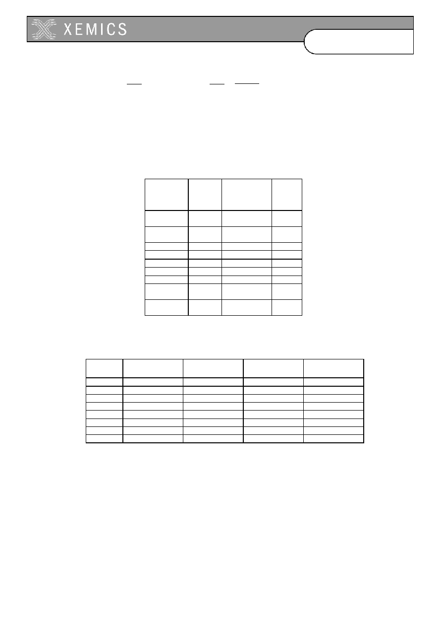
16-17
D0304-40
Datasheet
XE88LC05/05A
-
=
IN
REF
TOT
TOT
REF
IN
ADC
V
V
GDoff
GD
V
V
OUT
16
2
OSR
OSR 1
+
(LSB) (Eq. 18)
where, from Eq. 10 and Eq. 11, the total PGA gain and offset are respectively:
1
2
3
GD
GD
GD
GD
TOT
=
(V/V)
and:
2
3
3
GDoff
GD
GDoff
GDoff
TOT
+
=
(V/V)
ADC Input
Voltage
V
IN,ADC
% of
Full
Scale
(FS)
Output in
LSBs
Output
Code
in Hex
+2.49505V
+0.5
FS
+2
15
-1
=+32'767
7FFF
+2.49497V ...
+2
15
-2
=+32'766
7FFE
... ... ... ...
+76.145
µ
V
... +1
0001
0V 0 0 0000
-76.145
µ
V
... -1
FFFF
... ... ... ...
-2.49505V ...
-2
15
-1
=-32'767
8001
-2.49513V
-0.5
FS
-2
15
=-32'768
8000
Table 16-24. Basic ADC Relationships (example for: V
REF
= 5V, OSR = 512, n = 16 bits)
SET_OSR
[2:0]
SET_NELC = 00
SET_NELC = 01
SET_NELC = 10
SET_NELC = 11
000 1000000000
100000000 10000000 1000000
001 10000000
1000000 100000 10000
010 100000
10000 1000 100
011 1000
100 10 1
100 10 1 - -
101
- - - -
110
- - - -
111
- - - -
Table 16-25. Last forced LSBs in conversion output registers for resolution settings
smaller than 16 bits (n < 16) (
RegAcOutMsb[7:0]
&
RegAcOutLsb[7:0]
)

16-18
D0304-40
Datasheet
XE88LC05/05A
The equivalent LSB size at the input of the PGA chain is:
1
2
1
+
=
OSR
OSR
GD
V
LSB
TOT
REF
n
(V)
(Eq.
19)
Notice that the input voltage V
IN,ADC
of the ADC must satisfy the condition:
1
)
(
2
1
,
+
-
OSR
OSR
V
V
V
REFN
REFP
ADC
IN
(V)
(Eq.
20)
to remain within the ADC input range.
16.7.8
Power Saving Modes
During low-speed operation, the bias current in the PGAs and ADC can be programmed to save
power using the control words
IB_AMP_PGA[1:0]
and
IB_AMP_ADC[1:0]
(see Table 16-26). If the
system is idle, the PGAs and ADC can even be disabled, thus, reducing power consumption to its
minimum. This can considerably improve battery lifetime.
IB_AMP_ADC
[1:0]
IB_AMP_PGA
[1:0]
ADC
Bias
Current
PGA
Bias
Current
Max. f
S
[kHz]
00
01
10
11
x
1/4
I
ADC
1/2
I
ADC
3/4
I
ADC
I
ADC
x
62.5
125
250
500
x
00
01
10
11
x
1/4
I
PGA
1/2
I
PGA
3/4
I
PGA
I
PGA
62.5
125
250
500
Table 16-26. ADC & PGA power saving modes and maximum sampling frequency
16.8 Specifications and Measured Curves
This section presents measurement results for the acquisition chain. A summary table with circuit
specifications and measured curves are given.

16-19
D0304-40
Datasheet
XE88LC05/05A
16.8.1 Default
Settings
Unless otherwise specified, the measurement conditions are the following:
∑
Temperature T
A
= +25∞C
∑
V
DD
= +5V, GND = 0V, V
REF
= +5V, V
IN
= 0V
∑
RC frequency f
RC
= 2MHz, sampling frequency f
S
= 500kHz
∑
Offsets GDOff
2
= GDOff
3
= 0
∑
Power operation: normal (
IB_AMP_ADC[1:0]
=
IB_AMP_PGA[1:0]
= '11')
∑
Resolution:
for n = 12 bits: OSR = 32 and N
ELCONV
= 4
for
n = 16 bits: OSR = 512 and N
ELCONV
= 2

16-20
D0304-40
Datasheet
XE88LC05/05A
16.8.2 Specifications
Unless otherwise specified: Temperature T
A
= +25∞C, V
DD
= +5V, GND = 0V, V
REF
= +5V, V
IN
= 0V, RC frequency f
RC
= 2MHz,
sampling frequency f
S
= 500kHz, Overall PGA gain GD
TOT
= 1, offsets GDOff
2
= GDOff
3
= 0. Power operation: normal
(
IB_AMP_ADC[1:0]
=
IB_AMP_PGA[1:0]
= '11'). For resolution n = 12 bits: OSR = 32 and N
ELCONV
= 4. For resolution n = 16
bits: OSR = 512 and N
ELCONV
= 2.
VALUE
PARAMETER
MIN TYP MAX
UNITS COMMENTS/CONDITIONS
ANALOG INPUT
CHARACTERISTICS
Differential Input Voltage Ranges
V
IN
= (V
INP
- V
INN
)
Reference Voltage Range
V
REF
= (V
REFP
≠ V
REFN
)
-2.42
-24.2
-2.42
+2.42
+24.2
+2.42
V
DD
V
mV
mV
V
Gain = 1, OSR = 32 (Note 1)
Gain = 100, OSR = 32
Gain = 1000, OSR = 32
PROGRAMMABLE GAIN
AMPLIFIERS (PGA)
Total PGA Gain, GD
TOT
PGA1 Gain, GD
1
PGA2 Gain, GD
2
PGA3 Gain, GD
3
Gain Setting Precision (each stage)
Gain Temperature Dependence
Offset
PGA2 Offset, GDoff
2
PGA3 Offset, GDoff
3
Offset Setting Precision (PGA2 or 3)
Offset Temperature Dependence
Input Impedance
PGA1
PGA2,
PGA3
Output RMS Noise
PGA1
PGA2
PGA3
0.5
1
1
0
-3
-1
-127/12
-3
1500
150
150
±
0.5
±
5
±
0.5
±
5
205
340
365
1000
10
10
127/12
+3
+1
+127/12
+3
V/V
V/V
V/V
V/V
%
ppm/∞C
V/V
V/V
%
ppm/∞C
k
k
k
µ
V
µ
V
µ
V
See Table 16-14
See Table 16-15
Step=1/12 V/V, See Table
16-17
Step=0.2 V/V, See Table 16-16
Step=1/12 V/V, See Table
16-18
(Note 2)
PGA1 Gain = 1 (Note 3)
PGA1 Gain = 10 (Note 3)
Maximal gain (Note 3)
(Note 4)
(Note 5)
(Note 6)
ADC STATIC PERFORMANCE
Resolution, n
No Missing Codes
Gain Error
Offset Error
Integral Non-Linearity, INL
Resolution n = 16 Bits
Differential Non-Linearity, DNL
Resolution n = 16 Bits
Power Supply Rejection Ratio, PSRR
6
±
0.15
±
1
±
1.0
±
0.5
78
72
16
Bits
% of FS
LSB
LSB
LSB
dB
dB
(Note 7)
(Note 8)
(Note 9)
n = 16 bits (Note 10)
(Note 11)
(Note 12)
V
DD
= 5V
±
0.3V (Note 13)
V
DD
= 3V
±
0.3V (Note 13)
DYNAMIC PERFORMANCE
Sampling Frequency, f
S
Conversion Time, T
CONV
Throughput Rate (Continuous Mode),
1/T
CONV
Nbr of Initialization Cycles, N
INIT
Nbr of End Conversion Cycles, N
END
PGA Stabilization Delay
3
0
0
133
1027
3.76
0.49
OSR
2
5
kHz
cycles/f
S
cycles/f
S
kSps
kSps
cycles
cycles
cycles
n = 12 bits (Note 14)
n = 16 bits (Note 14)
n = 12 bits, f
S
= 500kHz
n = 16 bits, f
S
= 500kHz
(Note 15)
DIGITAL OUTPUT
ADC Output Data Coding
Binary Two's Complement
See Table 16-24 and Table
16-25

16-21
D0304-40
Datasheet
XE88LC05/05A
Specifications (Cont'd)
VALUE
PARAMETER
MIN TYP MAX
UNITS COMMENTS/CONDITIONS
POWER SUPPLY
Voltage Supply Range, V
DD
Analog Quiescent Current
Consumption, Total (I
Q
)
ADC Only
PGA1
PGA2
PGA3
Analog Power Dissipation
Normal Power Mode
3/4 Power Reduction Mode
1/2 Power Reduction Mode
1/4 Power Reduction Mode
+2.4
+5
720/620
250/190
165/150
130/120
175/160
3.6/1.9
2.7/1.4
1.8/0.9
0.9/0.5
+5.5
V
µ
A
µ
A
µ
A
µ
A
µ
A
mW
mW
mW
mW
Only Acquisition Chain
V
DD
= 5V/3V
V
DD
= 5V/3V
V
DD
= 5V/3V
V
DD
= 5V/3V
V
DD
= 5V/3V
All PGAs & ADC Active
V
DD
= 5V/3V (Note 16)
V
DD
= 5V/3V (Note 17)
V
DD
= 5V/3V (Note 18)
V
DD
= 5V/3V (Note 19)
TEMPERATURE
Specified Range
Operating Range
-40
-40
+85
+125
∞C
∞C
Notes:
(1) Gain defined as overall PGA gain GD
TOT
= GD
1
GD
2
GD
3
. Maximum input voltage is given by:
V
IN,MAX
=
±
(V
REF
/2)
(OSR/OSR+1).
(2) Offset due to tolerance on GDoff
2
or GDoff
3
setting. For small intrinsic offset, use only ADC and PGA1.
(3) Measured with block connected to inputs through AMUX block. Normalized input sampling frequency for input
impedance is f
S
= 512kHz. This figure must be multiplied by 2 for f
S
= 256kHz, 4 for f
S
= 128kHz. Input impedance is
proportional to 1/f
S
.
(4)
Figure independent from PGA1 gain and sampling frequency f
S
. See model of Figure 16-18(a).
See equation Eq. 21 to calculate equivalent input noise.
(5) Figure independent on PGA2 gain and sampling frequency f
S
. See model of Figure 16-18(a). See equation Eq. 21
to calculate equivalent input noise.
(6) Figure independent on PGA3 gain and sampling frequency f
S
. See model of Figure 16-18(a) and equation Eq. 21 to
calculate equivalent input noise.
(7) Resolution is given by n = 2
log2(OSR) + log2(N
ELCONV
). OSR can be set between 8 and 1024, in powers of 2.
N
ELCONV
can be set to 1, 2, 4 or 8.
(8) If a ramp signal is applied to the input, all digital codes appear in the resulting ADC output data.
(9) Gain error is defined as the amount of deviation between the ideal (theoretical) transfer function and the measured
transfer function (with the offset error removed). (See Figure 16-19)
(10) Offset error is defined as the output code error for a zero volt input (ideally, output code = 0). For
±
1 LSB offset,
N
ELCONV
must be
2.
(11) INL defined as the deviation of the DC transfer curve of each individual code from the best-fit straight line. This
specification holds over the full scale.
(12) DNL is defined as the difference (in LSB) between the ideal (1 LSB) and measured code transitions for successive
codes.
(13) Figures for Gains = 1 to 100. PSRR is defined as the amount of change in the ADC output value as the power
supply voltage changes.
(14) Conversion time is given by: T
CONV
= (N
ELCONV
(OSR + 1) + 1) / f
S
. OSR can be set between 8 and 1024, in powers
of 2. N
ELCONV
can be set to 1, 2, 4 or 8.
(15) PGAs are reset after each writing operation to registers
RegAcCfg1-5
. The ADC must be started after a PGA or
inputs common-mode stabilisation delay. This is done by writing bit
Start
several cycles after PGA settings
modification or channel switching. Delay between PGA start or input channel switching and ADC start should be
equivalent to OSR (between 8 and 1024) number of cycles. This delay does not apply to conversions made without
the PGAs.
(16) Nominal (maximum) bias currents in PGAs and ADC, i.e.
IB_AMP_PGA[1:0]
= `11' and
IB_AMP_ADC[1:0]
=
`11'.
(17) Bias currents in PGAs and ADC set to 3/4 of nominal values, i.e.
IB_AMP_PGA[1:0]
= `10',
IB_AMP_ADC[1:0]
=
`10'.
(18) Bias currents in PGAs and ADC set to 1/2 of nominal values, i.e.
IB_AMP_PGA[1:0]
= `01',
IB_AMP_ADC[1:0]
=
`01'.
(19) Bias currents in PGAs and ADC set to 1/4 of nominal values, i.e.
IB_AMP_PGA[1:0]
= `00',
IB_AMP_ADC[1:0]
=
`00'.

16-22
D0304-40
Datasheet
XE88LC05/05A
16.8.3 Linearity
16.8.3.1 Integral
non-linearity
The integral non-linearity depends on the selected gain configuration. First of all, the non-linearity of
the ADC (all PGA stages bypassed) is shown in Figure 16-8.
Figure 16-8. Integral non-linearity of the ADC (PGA disabled, reference voltage of 4.8V)
The different PGA stages have been designed to find the best compromise between the noise
performance, the integral non-linearity and the power consumption. To obtain this, the first stage has
the best noise performance and the third stage the best linearity performance. For large input signals
(small PGA gains, i.e. up to about 50), the noise added by the PGA is very small with respect to the
input signal and the second and third stage of the PGA should be used to get the best linearity. For
small input signals (large gains, i.e. above 50), the noise level in the PGA is important and the first
stage of the PGA should be used.
The following figures give the non-linearity for different gain settings of the PGA, selecting the
appropriate stage to get the best noise and linearity performance. Figure 16-9 shows the non-linearity
when the third stage is used with a gain of 1. It is of course not very useful to use the PGA with a gain
of 1 unless it is used to compensate offset. By increasing the gain, the integral non-linearity becomes
even smaller since the signal in the amplifiers reduces.
Figure 16-10 shows the non-linearity for a gain of 2. Figure 16-11 shows the non-linearity for a gain of
5. Figure 16-12 shows the non-linearity for a gain of 10. By comparing these figures to Figure 16-8, it
can be seen that the third stage of the PGA does not add significant integral non-linearity.
Figure 16-13 shows the non-linearity for a gain of 20 and Figure 16-14 shows the non-linearity for a
gain of 50. In both cases the PGA2 is used at a gain of 10 and the remaining gain is realized by the
third stage. It can be seen again that the second stage of the PGA does not add significant non-
linearity.
For gains above 50, the first stage PGA1 should be selected in stead of PGA2. Although the non-
linearity in the first stage of the PGA is larger than in stage 2 and 3, the gain in stage 3 is now
sufficiently high so that the non-linearity of the first stage does become negligible as is shown in
Figure 16-15 for a gain of 100. Therefor, the first stage is preferred over the second stage since it has
less noise.
Increasing the gain further up to 1000 will further increase the linearity since the signal becomes very
small in the first two stages. The signal is full scale at the output of stage 3 and as shown in Figure
16-9 to Figure 16-12, this stage has very good linearity.

16-23
D0304-40
Datasheet
XE88LC05/05A
Figure 16-9. Integral non-linearity of the ADC and with gain of 1 (PGA1 and PGA2
disabled, PGA3=1, reference voltage of 5V)
Figure 16-10. Integral non-linearity of the ADC and gain of 2 (PGA1 and PGA2 disabled,
PGA3=2 reference voltage of 5V)
Figure 16-11. Integral non-linearity of the ADC and gain of 5 (PGA1 and PGA2 disabled,
PGA3=5, reference voltage of 5V)
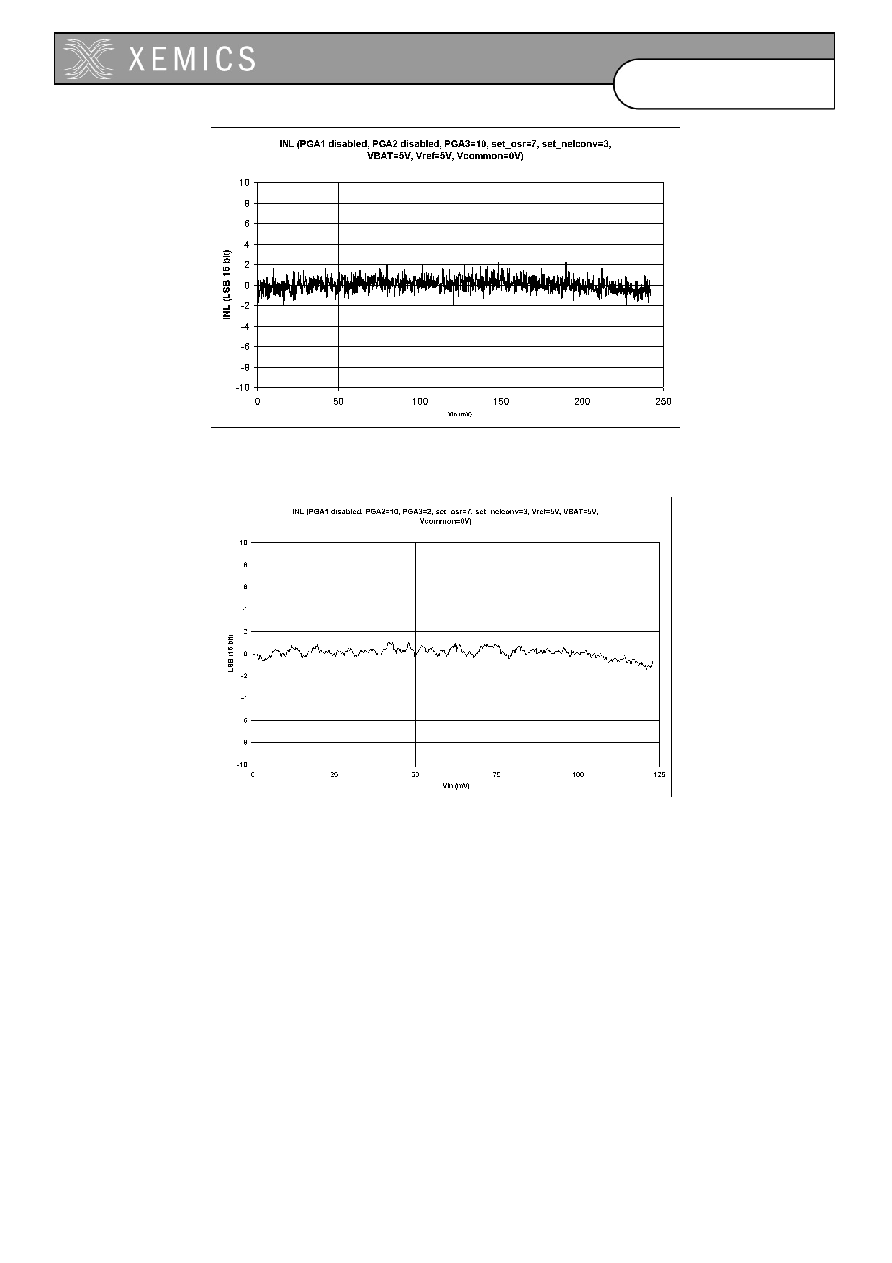
16-24
D0304-40
Datasheet
XE88LC05/05A
Figure 16-12. Integral non-linearity of the ADC and gain of 10 (PGA1 and PGA2 disabled,
PGA3=10, reference voltage of 5V)
Figure 16-13. Integral non-linearity of the ADC and gain of 20 (PGA1 and PGA2=10,
PGA3=2, reference voltage of 5V)
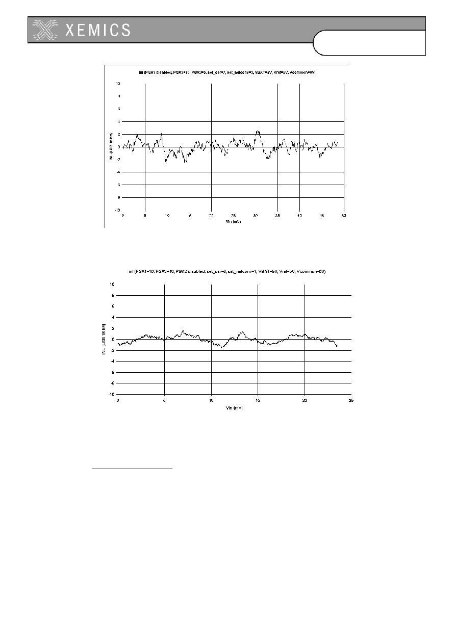
16-25
D0304-40
Datasheet
XE88LC05/05A
Figure 16-14. Integral non-linearity of the ADC and gain of 50 (PGA1 disabled, PGA2=10,
PGA3=5, reference voltage of 5V)
Figure 16-15. Integral non-linearity of the ADC and gain of 100 (PGA1=10 and PGA3=10,
PGA2 disabled, reference voltage of 5V)
16.8.3.2 Differential
non-linearity
The differential non-linearity is generated by the ADC. The PGA does not add differential non-linearity.
Figure 16-16 shows the differential non-linearity.

16-26
D0304-40
Datasheet
XE88LC05/05A
Figure 16-16. Differential non-linearity of the ADC converter.
16.8.4 Noise
Ideally, a constant input voltage V
IN
should result in a constant output code. However, because of
circuit noise, the output code may vary for a fixed input voltage. Thus, a statistical analysis on the
output code of 1200 conversions for a constant input voltage was performed to derive the equivalent
noise levels of PGA1, PGA2, and PGA3. The extracted rms output noise of PGA1, 2, and 3 are given
in Table 16-27: standard output deviation and output rms noise voltage. Figure 16-17 shows the
distribution for the ADC alone (PGA1, 2, and 3 bypassed). Quantization noise is dominant in this case,
and, thus, the ADC thermal noise is below 16 bits.
The simple noise model of Figure 16-18(a) is used to estimate the equivalent input referred rms noise
V
N,IN
of the acquisition chain in the model of Figure 16-18(b). This is given by the relationship:
)
(
))
/(
(
))
/(
(
)
/
(
2
3
2
1
3
2
2
1
2
2
1
1
2
,
ELCONV
N
N
N
IN
N
N
OSR
GD
GD
GD
V
GD
GD
V
GD
V
V
+
+
=
(V
2
rms) (Eq.
21)
where V
N1
, V
N2
, and V
N3
are the output rms noise figures of Table 16-27, GD
1
, GD
2
, and GD
3
are the
PGA gains of stages 1 to 3 respectively. As shown in this equation, noise can be reduced by
increasing OSR and N
ELCONV
(increases the ADC averaging effect, but reduces noise).
Parameter
PGA1 PGA2 PGA3
Standard deviation at
ADC output (LSB)
0.85
1.4
1.5
Output rms noise (
µ
V)
1
205 (V
N1
)
340
(V
N2
)
365
(V
N3
)
Note: see noise model of Figure 16-18 and equation Eq. 21.
Table 16-27. PGA noise measurements (n = 16 bits, OSR = 512, N
ELCONV
= 2, V
REF
= 5V)

16-27
D0304-40
Datasheet
XE88LC05/05A
0
20
40
60
80
-5
-4
-3
-2
-1
0
1
2
3
4
5
Output Code Deviation From Mean Value [LSB]
Oc
curence
s
[
%
o
f
to
t
a
l s
a
m
p
les
]
Figure 16-17. ADC noise (PGA1, 2 & 3 bypassed, OSR=512,N
ELCONV
=2)
PGA1
PGA2
PGA3
ADC
GD1
GD2
GD3
V
N1
f
S
V
N2
V
N3
(a)
PGA1
PGA2
PGA3
ADC
GD1
GD2
GD3
V
N,IN
f
S
(b)
Figure 16-18. (a) Simple noise model for PGAs and ADC
and (b) total input referred noise
As an example, consider the system where: GD
2
= 10 (GD
1
= 1; PGA3 bypassed), OSR = 512,
N
ELCONV
= 2, V
REF
= 5V. In this case, the noise contribution V
N1
of PGA1 is dominant over that of
PGA2. Using equation Eq. 21, we get: V
N,IN
= 6.4
µ
V (rms) at the input of the acquisition chain, or,
equivalently, 0.85 LSB at the output of the ADC. Considering a 0.2V (rms) maximum signal amplitude,
the signal-to-noise ratio is 90dB.
Noise can also be reduced by implementing a software filter. By making an average on a number of
subsequent measurements, the apparent noise is reduced the square root of the number of
measurement used to make the average.
16.8.5
Gain Error and Offset Error
Gain error is defined as the amount of deviation between the ideal transfer function (theoretical
equation Eq. 18) and the measured transfer function (with the offset error removed).
The actual gain of the different stages can vary depending on the fabrication tolerances of the
different elements. Although these tolerances are specified to a maximum of
±
3%, they will be most of
the time around
±
0.5%. Moreover, the tolerances between the different stages are not correlated and
the probability to get the maximal error in the same direction in all stages is very low. Finally, these
gain errors can be calibrated by the software at the same time with the gain errors of the sensor for
instance.
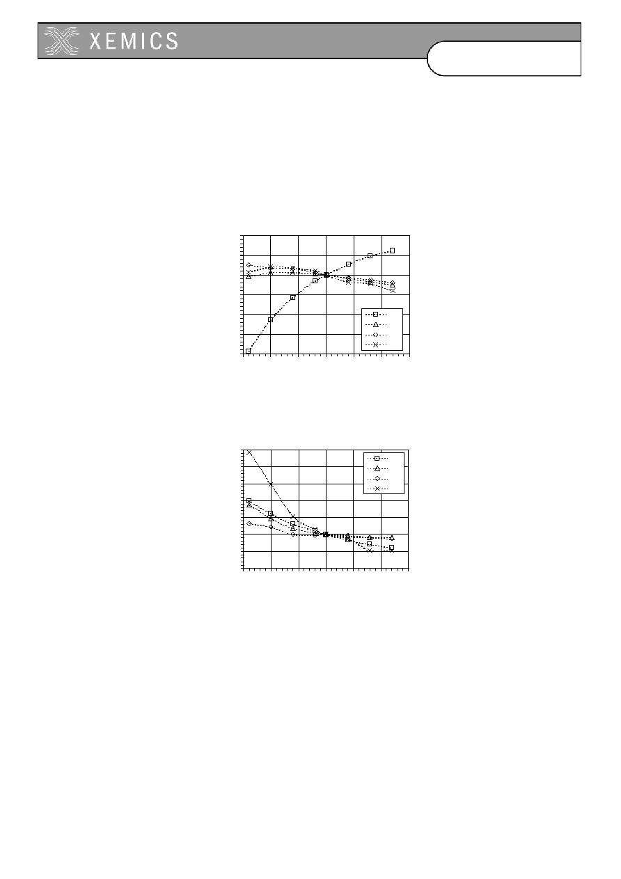
16-28
D0304-40
Datasheet
XE88LC05/05A
Figure 16-19 shows gain error drift vs. temperature for different PGA gains. The curves are expressed
in % of Full-Scale Range (FSR) normalized to 25∞C.
Offset error is defined as the output code error for a zero volt input (ideally, output code = 0). The
offset of the ADC and the PGA1 stage are completely suppressed if N
ELCONV
> 1.
The measured offset drift vs. temperature curves for different PGA gains are depicted in Figure 16-20.
The output offset error, expressed in LSB for 16-bit setting, is normalized to 25∞C. Notice that if the
ADC is used alone, the output offset error is below
±
1 LSB and has no drift.
NORMALIZED TO 25∞C
-0.4
-0.3
-0.2
-0.1
0.0
0.1
0.2
-50
-25
0
25
50
75
100
Temperature [∞C]
G
a
in
E
r
r
o
r
[%
o
f
F
S
R
]
1
5
20
100
Figure 16-19. Gain error vs. temperature for different PGA gains
NORMALIZED TO 25∞C
-40
-20
0
20
40
60
80
100
-50
-25
0
25
50
75
100
Temperature [∞C]
O
u
tp
u
t
O
f
fs
e
t
E
r
r
o
r
[L
S
B
]
1
5
20
100
Figure 16-20. Offset error vs. temperature for different PGA gains
16.8.6 Power
Consumption
Figure 16-21 plots the variation of quiescent current consumption with supply voltage V
DD
, as well as
the distribution between the 3 PGA stages and the ADC (see Table 16-28). As shown in Figure 16-22,
if lower sampling frequency is used, the quiescent current consumption can be lowered by reducing
the bias currents of the PGAs and the ADC with registers
IB_AMP_PGA [1:0]
and
IB_AMP_ADC
[1:0]
. (In Figure 16-22,
IB_AMP_PGA/ADC[1:0]
= '11', '10', '00' for f
S
= 500, 250, 62.5kHz
respectively.)
Quiescent current consumption vs. temperature is depicted in Figure 16-23, showing a relative
increase of nearly 40% between -45 and +85∞C. Figure 16-24 shows the variation of quiescent current
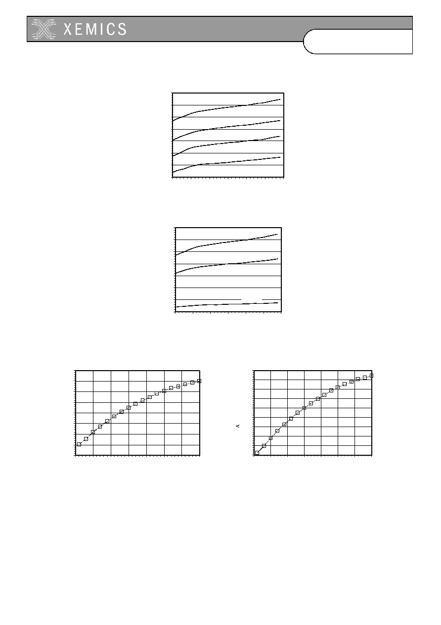
16-29
D0304-40
Datasheet
XE88LC05/05A
consumption for different frequency settings of the internal RC oscillator. It can be seen that the
quiescent current varies by about 20% between 100kHz and 2MHz.
100
200
300
400
500
600
700
800
2.5
3.0
3.5
4.0
4.5
5.0
5.5
Supply Voltage - V
DDA
[V]
Q
u
i
e
s
c
e
n
t C
u
r
r
e
n
t
- I
Q
[
µ
A]
No PGAs, ADC only
PGA1 + ADC
PGA1 & 2 + ADC
PGA1, 2 & 3 + ADC
Figure 16-21. Quiescent current consumption vs. supply voltage
100
200
300
400
500
600
700
800
2.5
3.0
3.5
4.0
4.5
5.0
5.5
Supply Voltage - V
DDA
[V]
Q
u
i
e
s
c
e
n
t Cu
r
r
e
n
t
- I
Q
[
µ
A]
500kHz
Sampling Frequency f
S
:
250kHz
62.5kHz
Figure 16-22. Quiescent current consumption vs. supply voltage for different sampling
frequencies
500
550
600
650
700
750
800
850
900
-50
-25
0
25
50
75
100
125
Temperature [∞C]
Q
u
ie
s
c
e
n
t C
u
r
r
e
n
t
-
I
Q
[
µ
A]
-25
-20
-15
-10
-5
0
5
10
15
20
-50
-25
0
25
50
75
100
125
Temperature [∞C]
R
e
l
a
t
i
ve
Q
u
i
e
s
c
en
t
C
u
r
r
en
t
C
h
a
n
g
e
I
Q
/ I
Q,
2
5
∞
C
[%
]
(a)
(b)
Figure 16-23. (a) Absolute and (b) relative change inquiescent current consumption vs.
temperature
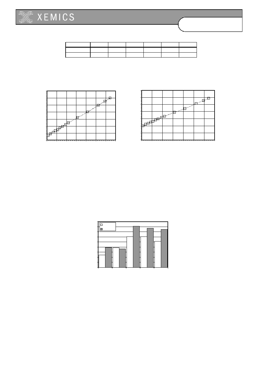
16-30
D0304-40
Datasheet
XE88LC05/05A
Supply
ADC PGA1 PGA2
PGA3 TOTAL Unit
V
DD
= 5V
250
165 130 175 720
µ
A
V
DD
= 3V
190
150 120 160 620
µ
A
Table 16-28. Typical quiescent current distributions in acquisition chain (n = 16 bits, f
S
=
500kHz)
-20
-15
-10
-5
0
5
10
15
0
500
1000
1500
2000
2500
3000
3500
Frequency - f
RC
[kHz]
Rel
a
t
i
v
e
Q
u
i
e
sc
en
t
Cur
r
ent
Chan
ge
I
Q
/
I
Q,
2
M
H
z
[%
]
500
550
600
650
700
750
800
850
0
500
1000
1500
2000
2500
3000
3500
Frequency - f
RC
[kHz]
Q
u
i
esc
ent
C
u
r
r
e
nt
-
I
Q
[
µ
A]
(a)
(b)
Figure 16-24. (a) Absolute and (b) relative change in quiescent curent consumption vs.
RC oscillator frequency (all PGAs active, V
DD
= 5V)
16.8.7
Power Supply Rejection Ratio
Figure 16-25 shows power supply rejection ratio (PSRR) at 3V and 5V supply voltage, and for various
PGA gains. PSRR is defined as the ratio (in dB) of voltage supply change (in V) to the change in the
converter output (in V). PSRR depends on both PGA gain and supply voltage V
DD
.
60
65
70
75
80
85
90
95
100
105
1
5
10
20
100
PGA Gain [V/V]
PS
RR [
d
B]
VDD=3V
VDD=5V
Figure 16-25. Power supply rejection ratio (PSRR)

16-31
D0304-40
Datasheet
XE88LC05/05A
Supply
GAIN = 1
GAIN =5
GAIN = 10
GAIN = 20
GAIN =100
Unit
V
DD
= 5V
79
78
100
99
97
dB
V
DD
=
3V
72 79 90 90 86
dB
Table 16-29. PSRR (n = 16 bits, V
IN
= V
REF
= 2.5V, f
S
= 500kHz)
16.9 Application
Hints
16.9.1 Input
Impedance
The PGAs of the acquisition chain employ switched-capacitor techniques. For this reason, while a
conversion is done, the input impedance on the selected channel of the PGAs is inversely proportional
to the sampling frequency f
S
and to stage gain as given in equation 22.
gain
f
Hz
Z
s
in
9
10
768
(Eq.
22)
The input impedance observed is the input impedance of the first PGA stage that is enabled or the
input impedance of the ADC if all three stages are disabled.
PGA1 (with a gain of 10), PGA2 (with a gain of 10) and PGA3 (with a gain of 10) each have a
minimum input impedance of 150k
at f
S
= 512kHz (see Specification Table). Larger input impedance
can be obtained by reducing the gain and/or by reducing the sampling frequency. Therefor, with a
gain of 1 and a sampling frequency of 100kHz, Z
in
> 7.6M
.
The input impedance on channels that are not selected is very high (>100M
).
16.9.2
PGA Settling or Input Channel Modifications
PGAs are reset after each writing operation to registers
RegAcCfg1-5
. Similarly, input channels are
switched after modifications of
AMUX[4:0]
or
VMUX
. To ensure precise conversion, the ADC must be
started after a PGA or inputs common-mode stabilization delay. This is done by writing bit
START
several cycles after PGA settings modification or channel switching. Delay between PGA start or input
channel switching and ADC start should be equivalent to OSR (between 8 and 1024) number of
cycles. This delay does not apply to conversions made without the PGAs.
If the ADC is not settled within the specified period, there is most probably an input impedance
problem (see previous section).
16.9.3
PGA Gain & Offset, Linearity and Noise
Hereafter are a few design guidelines that should be taken into account when using the
ZoomingADC
:
1) Keep in mind that increasing the overall PGA gain, or "zooming" coefficient, improves
linearity but degrades noise performance.
2) Use the minimum number of PGA stages necessary to produce the desired gain ("zooming")
and offset. Bypass unnecessary PGAs.
3) For high gains (>50), use PGA stage 1. For low gains (<50) use stages 2 and 3.
4) For the lowest noise, set the highest possible gain on the first (front) PGA stage used in the
chain. For example, in an application where a gain of 20 is needed, set the gain of PGA2 to
10, set the gain of PGA3 to 2.

16-32
D0304-40
Datasheet
XE88LC05/05A
4) For highest linearity and lowest noise performance, bypass all PGAs and use the ADC alone
(applications where no "zooming" is needed); i.e. set
ENABLE[3:0]
= '0001'.
5) For low-noise applications where power consumption is not a primary concern, maintain the
largest bias currents in the PGAs and in the ADC; i.e. set
IB_AMP_PGA[1:0]
=
IB_AMP_ADC[1:0]
= '11'.
6) For lowest output offset error at the output of the ADC, bypass PGA2 and PGA3. Indeed,
PGA2 and PGA3 typically introduce an offset of about 5 to 10 LSB (16 bit) at their output.
Note, however, that the ADC output offset is easily calibrated out by software.
16.9.4 Frequency
Response
The incremental ADC is an over-sampled converter with two main blocks: an analog modulator and a
low-pass digital filter. The main function of the digital filter is to remove the quantization noise
introduced by the modulator. As shown in Figure 16-26, this filter determines the frequency response
of the transfer function between the output of the ADC and the analog input V
IN
. Notice that the
frequency axes are normalized to one elementary conversion period OSR/f
S
. The plots of Figure
16-26 also show that the frequency response changes with the number of elementary conversions
N
ELCONV
performed. In particular, notches appear for N
ELCONV
2. These notches occur at:
ELCONV
S
NOTCH
N
OSR
f
i
i
f
=
)
(
(Hz)
for
)
1
(
,...,
2
,
1
-
=
ELCONV
N
i
(Eq.
23)
and are repeated every f
S
/OSR.
Information on the location of these notches is particularly useful when specific frequencies must be
filtered out by the acquisition system. For example, consider a 5Hz-bandwidth, 16-bit sensing system
where 50Hz line rejection is needed. Using the above equation and the plots below, we set the 4th
notch for N
ELCONV
= 4 to 50Hz, i.e. 1.25
f
S
/OSR = 50Hz. The sampling frequency is then calculated as
f
S
= 20.48kHz for OSR = 512. Notice that this choice yields also good attenuation of 50Hz harmonics.
0
0.2
0.4
0.6
0.8
1
1.2
0
1
2
3
4
Normalized Frequency - f *(OSR/f
S
) [-]
N
o
r
m
a
l
iz
e
d
M
a
g
n
it
u
d
e
[
-
]
N
ELCONV
= 1
0
0.2
0.4
0.6
0.8
1
1.2
0
1
2
3
4
Normalized Frequency - f *(OSR/f
S
) [-]
N
o
r
m
a
l
i
z
e
d
M
a
g
n
i
t
u
d
e
[-]
N
ELCONV
= 2
0
0.2
0.4
0.6
0.8
1
1.2
0
1
2
3
4
Normalized Frequency - f *(OSR/f
S
) [-]
N
o
r
m
a
l
i
z
e
d
M
a
g
n
i
tu
d
e
[-]
N
ELCONV
= 4
0
0.2
0.4
0.6
0.8
1
1.2
0
1
2
3
4
Normalized Frequency - f *(OSR/f
S
) [-]
No
r
m
a
l
i
z
e
d
M
a
g
n
i
tu
d
e
[-]
N
ELCONV
= 8
Figure 16-26. Frequency response: normalized magnitude vs. frequency for different
N
ELCONV

16-33
D0304-40
Datasheet
XE88LC05/05A
16.9.5 Power
Reduction
The ZoominADC
is particularly well suited for low-power applications. When very low power
consumption is of primary concern, such as in battery operated systems, several parameters can be
used to reduce power consumption as follows:
1) Operate the acquisition chain with a reduced supply voltage V
DD
.
2) Disable the PGAs which are not used during analog-to-digital conversion with
ENABLE[3:0]
.
3) Disable all PGAs and the ADC when the system is idle and no conversion is performed.
4) Use lower bias currents in the PGAs and the ADC using the control words
IB_AMP_PGA[1:0]
and
IB_AMP_ADC[1:0]
. (This reduces the maximum sampling
frequency according to Table 16-26.)
5) Reduce internal RC oscillator frequency and/or sampling frequency.
Finally, remember that power reduction is typically traded off with reduced linearity, larger noise and
slower maximum sampling speed.

17-1
vmult_ff - 1.0 ≠ 11 october 2002
D0304-40
Datasheet
XE88LC05/05A
17. Vmult (Voltage Multiplier)
17.1
Features
17-2
17.2
Overview
17-2
17.3
Control register
17-2
17.4
External component
17-2

17-2
D0304-40
Datasheet
XE88LC05/05A
17.1 Features
∑
Generates a voltage that is higher or equal to the supply voltage.
∑
Can be easily enabled or disabled
17.2 Overview
The Vmult block generates a voltage (called "Vmult") that is higher or equal to the supply voltage. This
output voltage is used in the acquisition chain.
The voltage multiplier should be on (bit ENABLE in RegVmultCfg0) when using the acquisition chain
or analog properties of the Port B while VBAT is below 3V. If the multiplier is enabled, the external
capacitor on the pin VMULT is mandatory.
The source clock of Vmult is selected by FIN[1:0] in RegVmultCfg0. It is strongly recommended to
use the same settings as in the ADC.
17.3 Control
register
There is only one register in the Vmult. Table 177-1 describes the bits in the register.
Pos. RegVmultCfg0
rw
Reset
Function
2 Enable
rw
0
resetsystem
enable of the vmult
`1' : enabled
`0' : disabled
1-0 Fin
rw 0
resetsystem
system clock division factor
`00' : 1/2,
`01' : 1/4,
`10' : 1/16,
`11' : 1/64
Table 177-1. RegVmultCfg0
17.4 External
component
When the multiplier is enabled, a capacitor has to be connected to the VMULT pin. If the multiplier is
disabled, the pin may remain floating.
Min.
Max.
Note
Capacitor on VMULT
1.0
3.0
nF

18-1
das_ff - 1.0 ≠ 11 october 2002
D0304-40
Datasheet
XE88LC05/05A
18. Signal D/A (DAS)
18.1
Features
18-2
18.2
Overview of Signal DAC - The generic DAC
18-2
18.3
Registers Map
18-3
18.4
The D/A description
18-4
18.4.1
What is a noise shaper ?
18-4
18.4.2
Advantages/disadvantages 18-5
18.4.3
D/A setup and resolution
18-5
18.5
Amplifier
18-7
18.6
Low pass filter
18-8
18.6.1
First order low pass filter
18-8
18.6.2
Second order low pass filter
18-9
18.7
4-20mA loop
18-10
18.7.1
2-wire loop with first order filtering
18-10
18.7.2
2-wire loop with second order filtering
18-12
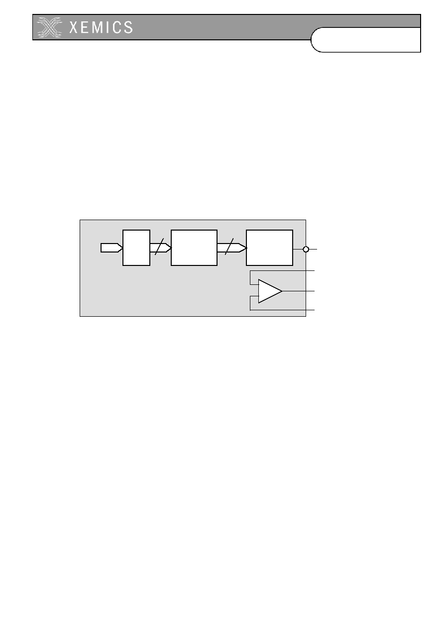
18-2
D0304-40
Datasheet
XE88LC05/05A
18.1 Features
∑
16-bits maximum input word width
∑
Synchronization mechanism to guarantee data integrity when writing LSB and MSB 8-bits
data
∑
Programmable noise shaper order: second, first or order zero
∑
Programmable PWM modulation between 4 and 11-bits
∑
Programmable clock input frequency: fin or fin/2
∑
Programmable output polarity: active high or low
∑
On chip amplifier for analog filtering, voltage output or 4-20 mA loop
18.2 Overview of Signal DAC - The generic DAC
The generic DAC block consists of two major parts: the noise shaper (sigma-delta modulator) and the
PWM modulator as shown in Figure 18-1.
control
Sigma-delta
modulator
PWM
modulator
CPU
bus
16
4-11
m
DAS Out
amp
Figure 18-1. General block diagram
A D/A converter that is built with a digital PWM modulator needs a high clock frequency for a small
signal bandwidth. For a 10 bit digital PWM modulator for instance, a 10 bit counter is needed in order
to create a pulse with a resolution of 1024. This means that, in case an infinitely sharp analog output
filter is used, the clock frequency has to be at least 1024 times the output bandwidth. In practice
however, in order to be able to build the analog filter, the clock frequency needs to be much higher.
In order to reduce this frequency requirement, the input digital word is broken down into n words with
a smaller width m by a noise shaper so that the "average" (average for first order noise shaper, more
complicated for higher order noise shapers) value of the n m-bit words represents the full width input
code. Instead of 1 pulse with the full resolution, the PWM modulator now generates n pulses with a
smaller resolution m. This increases the output pulse repetition frequency with a factor n for identical
clock frequency. Therefore, the analog output filtering is easier to implement. Higher order noise
shapers (order >1) allow to decrease the clock frequency for identical signal bandwidth.
Another advantage is that the signal distortion is less dependent on the signal value. A disadvantage
is however, that the output signal after filtering is more dependent on the rise and fall times of the
PWM output since there are many more pulses.
The maximum word width at the input is 16-bit. If the word is narrower, 0's have to be added after the
LSB. In order to maintain maximum flexibility, the order of the noise shaper and the resolution of the
PWM modulation are programmable by writing the codes CodeLmax and NsOrder to the
configuration register. The possible noise shaper order is 0 (which means no noise shaping), 1 or 2.
The possible PWM modulation resolution m can be set between 4 and 11.
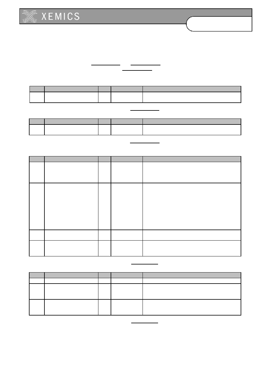
18-3
D0304-40
Datasheet
XE88LC05/05A
18.3 Registers Map
All registers are reset with the system reset.
The contents of the registers RegDasInLsb and RegDasInMsb are transferred to the D/A converter
when after data have been written into RegDasInMsb. Therefore, in order to maintain the
synchronisation between the LSB and MSB, the LSB should always be written before the MSB.
Pos. RegDasInLsb
rw
reset
function
7-0 DasInLsb(7:0)
rw 0
resetsystem
Data to convert LSB
Table 18-1. RegDasInLsb
Pos. RegDasInMsb
rw
reset
function
7-0 DasInMsb(7:0)
rw 0
resetsystem
Data to convert MSB
Table 18-2. RegDasInMsb
Pos. RegDasCfg0
rw
reset
function
7:6
NsOrder(1:0)
rw
00
resetsystem
Noise Shaper order
00 : order 0
01 : order 1
1x : order 2
5:3
CodeLmax(2:0)
rw
000
resetsystem
PWM pulse resolution :
000 : 4 bits
001 : 5 bits
010 : 6 bits
011 : 7 bits
100 : 8 bits
101 : 9 bits
110 : 10 bits
111 : 11 bits
2:1
Enable(1:0)
rw
00
resetsystem
Bit 0 : enables the D/A
Bit 1 : enables the amplifier
0
Fin
rw
0
resetsystem
Input frequency of modulator as a fraction of
oscillator frequency
0 : 1.f
RC
, 1 : Ω.f
RC
Table 18-3. RegDasCfg0
Pos. RegDasCfg1
rw
reset
function
7:2 -
rw 000000
Unused
1 BW
rw
0
resetsystem
Amplifier bandwidth
0 : small bandwidth
1 : large bandwidth
0 INV
rw
0
resetsystem
Inverts the PWM output
0 : normal, active high
1 : inverted, active low
Table 18-4. RegDasCfg1

18-4
D0304-40
Datasheet
XE88LC05/05A
18.4 The D/A description
The D/A converter consists of 2 parts: a classic PWM modulator which is preceded by a noise shaper
(Figure 18-1). The PWM signal has then to be low pass filtered using the amplifier and external
components to obtain the analog signal.
18.4.1
What is a noise shaper?
The major disadvantage of using a PWM modulator to generate a high resolution analog signal is that
it requires a high ratio between the PWM switching frequency and the useful bandwidth of the output
analog signal after low pass filtering.
Example: assuming the switching frequency of the PWM modulator is 1MHz and one wants to resolve
16 bit, i.e. 2
16
=65536 steps. In this case, the PWM has to code each step in increments of
1µs=1/1MHz and needs therefore 65536µs per pulse. This means that the PWM pulse repetition rate
is 1/65536µs=15.25Hz. So, even with a higher order low pass filter, more than 1 frequency decade
will be required to filter the PWM signal down to a 16 bit accurate analog signal. This leaves a useful
bandwidth below 1Hz.
The goal of the noise shaper is to reduce the ratio between the PWM switching frequency and the
useful bandwidth. The noise shaper will not reduce the "truncation noise" and "PWM modulation
noise" but move it to higher frequencies. It "shapes" the frequency spectrum ("noise") of the generated
PWM signal, hence its name. In practice, the noise shaper allows the generation of a signal with a
given resolution using a PWM modulator that has a lower resolution. The noise shaper then
generates a series of different subsequent low resolution codes for the PWM so that the average
value corresponds to the high resolution code.
The first order noise shaper interpolates between two adjacent PWM codes to obtain a higher
resolution. The second order noise shaper can use non-adjacent PWM codes.
Example for first order noise shaper: assuming again the resolution of 16 bits using a 1MHz PWM
switching frequency using the noise shaper with order 1. If a PWM modulator with 4 bits, i.e. 16 steps
is used, the PWM repetition frequency becomes then 1MHz/16=62.5kHz. The PWM modulator can
convert only the 4 MSB's of the 16 bit input such as h0000, h1000 until hF000. In order to convert the
code h5800, which is between h5000 and h6000? In this case, the first order noise shaper will
interpolate by presenting alternatively the code h5 and h6 to the PWM so that after filtering a signal is
obtained halfway between the normal PWM steps. To convert the code h5400, it will present h5 3
times and h6 once to the PWM and so on. It is clear from this that the PWM repetition frequency is
much higher than for the simple PWM and can be filtered out more easily. The quantization noise
frequency will depend on the code to be converted: for this example for instance we need two PWM
pulses to implement the code h5800, but we need four to implement h5400 etc.
Example for second order noise shaper: if we use the same conditions as for the example above, we
will obtain the same PWM repetition frequency. However, to implement the code h5400, the noise
shaper now can present the following sequence to the PWM modulator: h6, h5, h6, h4. This increases
the frequency components at the PWM pulse repetition frequency and Ω of the PWM pulse repetition
frequency but at the same time reduces energy at º of the PWM pulse repetition frequency with
respect to the first order noise shaper. The low pass cut-off frequency can therefore be higher than for
a first order noise shaper.
A disadvantage of the second order noise shaper is however that the resolution will drop when the
code is very close to h0000 or hFFFF.
Example: if we assume the same conditions as above, but we want to convert the code h0400. It is
now impossible to use a similar sequence as above (which would be h1, h0, h1, h(-1) ) due to
saturation of the code. There is no choice left but the sequence h1 h0 h0 h0 which is the same
sequence as in the first order noise shaper.

18-5
D0304-40
Datasheet
XE88LC05/05A
18.4.2 Advantages/disadvantages
Advantages:
Using a high order noise shaper together with a PWM modulator with low resolution reduces the ratio
between the low pass cut off frequency and the PWM switching frequency for the same total
resolution. This can be used to increase the output signal bandwidth or to reduce the PWM switching
frequency and therefore the power consumption of the D/A. Signal distortion is less dependent on the
signal value.
Disadvantages:
Using a high order noise shaper together with a PWM modulator with low resolution will use lots of
short pulses in stead of 1 long pulse. The D/A is therefore more sensitive to rise and fall times of the
PWM resulting in a slightly higher non-linearity and temperature dependence. The second order noise
shaper also has a reduced resolution for codes very close to zero or full scale.
18.4.3
D/A setup and resolution
In this section, the resolution that can be obtained with the D/A as a function of settings is calculated.
These calculations are based on the quantization and PWM modulation noise. Noise on the
reference, i.e. the supply voltage is not taken into account. High frequency noise on the supply
voltage can be filtered by the output low pass filter, but in band noise on the reference will show up in
the output signal with amplitude that will depend on the signal value. Therefore, when using the D/A,
one should take care to minimize the switching activity on the digital ports and/or to limit the load on
these ports.
18.4.3.1 Noise shaper of order 0
Setting the noise shaper to order 0 (NsOrder=00), reduces the D/A to a regular PWM. Two
parameters are setting the resolution of the D/A: the resolution of the modulator itself and the amount
of low pass filtering at the output.
The modulation width
m
of the PWM modulator is given by:
CodeLmax
+
=
4
m
The cut-off frequency
c
f
of the low pass filter required to get the resolution is calculated below. The
PWM modulator repetition frequency
PWM
f
can be calculated as a function of the selected
modulation width
m
, the frequency of the RC oscillator of the circuit
RC
f
and the selected frequency
division set by Fin :
m
RC
PWM
f
f
2
1
1
+
=
Fin
To obtain an analog signal with the required solution, the PWM signal has to be low pass filtered. The
resolution that can be obtained depends on the filter order and the ratio between the PWM modulation
frequency
PWM
f
and the filter cut-off frequency
c
f
. For a low pass filter of LpOrder, we obtain:
=
c
PWM
PWM
f
f
LpOrder
resolution
2
log
The total resolution of the D/A is then the minimal value of both criteria:
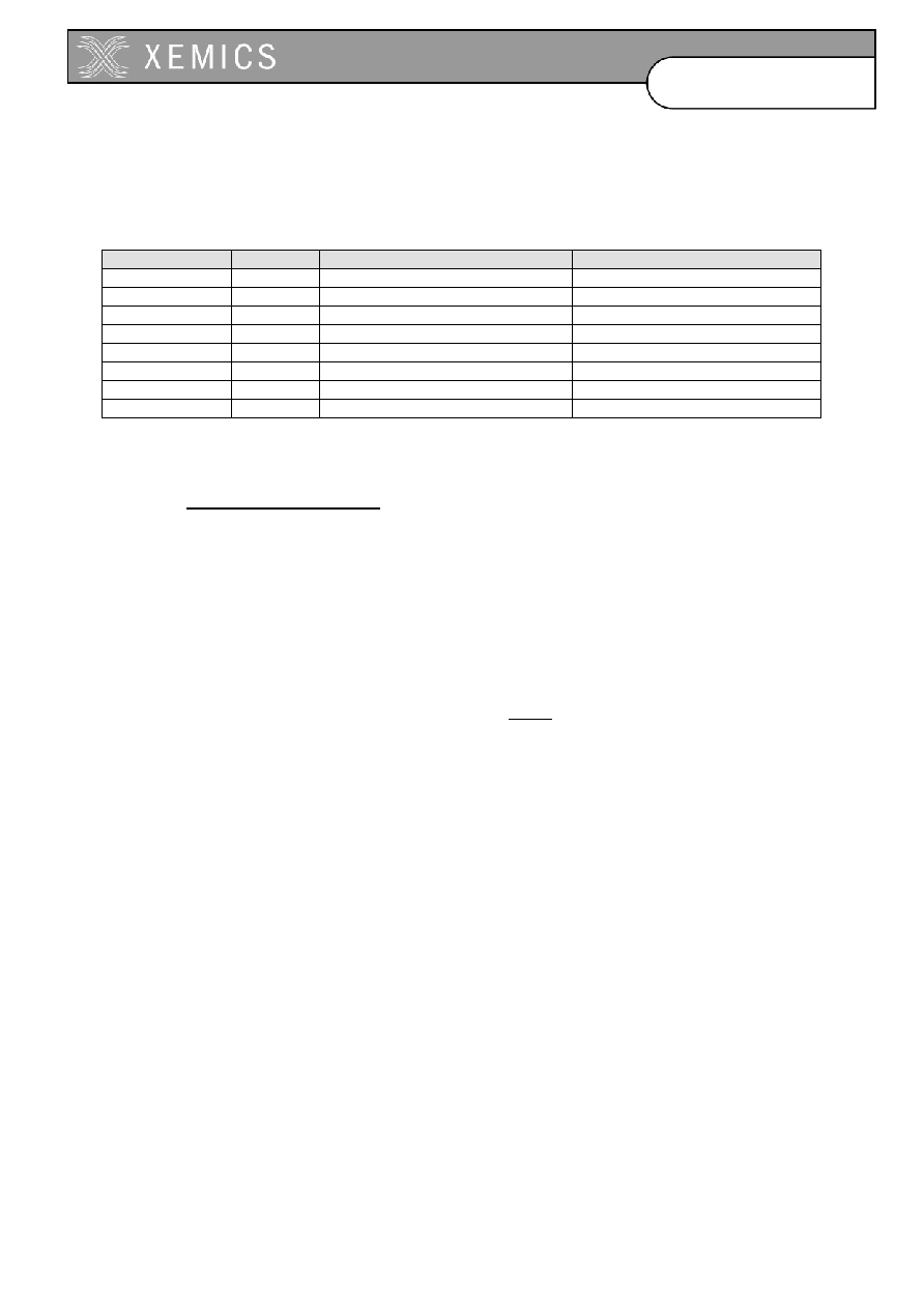
18-6
D0304-40
Datasheet
XE88LC05/05A
)
,
min(
PWM
resolution
m
resolution
=
In Table 18-5 the required cut-off frequency of the low pass filter is shown for a noise shaper of order
0 as a function of the desired resolution for both a first and second order low pass filter. The PWM
modulation factor m should be chosen equal to the desired resolution.
resolution (bit)
m
f
c
for LpOrder=1 (Hz)
f
c
for LpOrder=2 (Hz)
4 4
7812
31250
5 5
1953
11048
6 6
488
3906
7 7
122
1381
8 8
30
488
9 9
7.6
172
10 10
1.9
61
11 11
0.48
22
Table 18-5. Signal bandwidth as a function of the required resolution for the PWM without noise
shaper (Fin=0, NsOrder=00, f
RC
=2MHz).
18.4.3.2 Noise shaper of order 1 or 2
The calculation on the required low pass cut-off frequency given in 18.4.3.1 remains valid in this case.
However, the noise shaper allows using smaller PWM modulation for the same resolution. This
increases the PWM modulation frequency and as a consequence increases the output bandwidth.
An additional criterion however shows up: the filtering of the quantization noise. As can be seen from
the examples in 18.4.1, the interpolation between PWM codes generated by the noise shaper
introduce sequences at frequencies below the PWM modulation frequency. Assuming a low pass filter
that has at least the same order as the noise shaper, the resolution is given by (NsOrder1) :
-
+
+
=
65
.
2
)
(
log
359
.
0
2
c
PWM
quant
f
f
NsOrder
m
resolution
The total resolution of the D/A is then the minimal of both criteria:
)
,
min(
PWM
quant
resolution
resolution
resolution
=
Table 18-6 and Table 18-7 show the signal bandwidth that can be obtained as a function of required
resolution and PWM modulation for first and second order noise shapers. It can be seen that these
options are useful to obtain high resolution using low PWM modulation m. For high PWM modulation
m, the resolution is limited by the PWM modulator and adding a noise shaper does not change
anything.
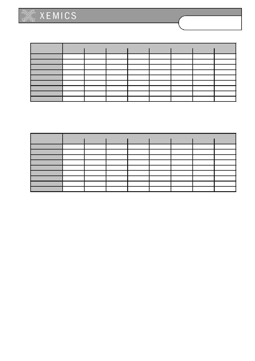
18-7
D0304-40
Datasheet
XE88LC05/05A
NsOrder=1, f
RC
=2MHz, Fin=0, LpOrder=2
Resolution
PWM modulation m
(bit)
4
5
6
7
8
9
10
11
8
1596.4
1596.4
1596.4
976.6
488.3
244.1
122.1
61.0
9
798.2
798.2
798.2
690.5
345.3
172.6
86.3
43.2
10
399.1
399.1
399.1
399.1
244.1
122.1
61.0
30.5
11
199.5
199.5
199.5
199.5
172.6
86.3
43.2
21.6
12
99.8
99.8
99.8
99.8
99.8
61.0
30.5
15.3
13
49.9
49.9
49.9
49.9
49.9
43.2
21.6
10.8
14
24.9
24.9
24.9
24.9
24.9
24.9
15.3
7.6
15
12.5
12.5
12.5
12.5
12.5
12.5
10.8
5.4
16
6.2
6.2
6.2
6.2
6.2
6.2
6.2
3.8
Table 18-6. Low pass cut-off frequency as a function of the selected PMW modulation and required
resolution for a first order noise shaper.
NsOrder=2, f
RC
=2MHz, Fin=0, LpOrder=2
Resolution
PWM modulation m
(bit)
4
5
6
7
8
9
10
11
8
5638.4
3906.3
1953.1
976.6
488.3
244.1
122.1
61.0
9
3986.9
2762.1
1381.1
690.5
345.3
172.6
86.3
43.2
10
2819.2
1953.1
976.6
488.3
244.1
122.1
61.0
30.5
11
1993.5
1381.1
690.5
345.3
172.6
86.3
43.2
21.6
12
1409.6
976.6
488.3
244.1
122.1
61.0
30.5
15.3
13
996.7
690.5
345.3
172.6
86.3
43.2
21.6
10.8
14
704.8
488.3
244.1
122.1
61.0
30.5
15.3
7.6
15
498.4
345.3
172.6
86.3
43.2
21.6
10.8
5.4
16
352.4
244.1
122.1
61.0
30.5
15.3
7.6
3.8
Table 18-7. Low pass cut-off frequency as a function of the selected MPW modulation and required
resolution for a second order noise shaper.
The output range of the D/A is for code 0h0000 is VSS and for code 0hFFFF is (VBAT-VSS)(2
m
-1)/2
m
.
18.5 Amplifier
The amplifier can be used to implement the low pass filter and/or a 4-20mA loop. The amplifier is
enabled using the bit Enable(1)=1. The amplifier has two different modes selected by the bit BW: a
low frequency mode (BW=0) that allows driving a high capacitive load and a high frequency mode
(BW=1).
The first mode is particularly adapted when a voltage output is used. The second mode is more
adapted for a 4-20mA loop since loads are small and higher bandwidth is required to reject current
consumption changes in the loop.
Table 18-8 shows the specification of the amplifier.
Note that the amplifier can not be used to generate signals that are larger than the supply voltages
VBAT and VSS since the amplifier inputs and outputs are clamped to these voltages. The amplifier
inputs and outputs should stay within the input and output ranges specified below.
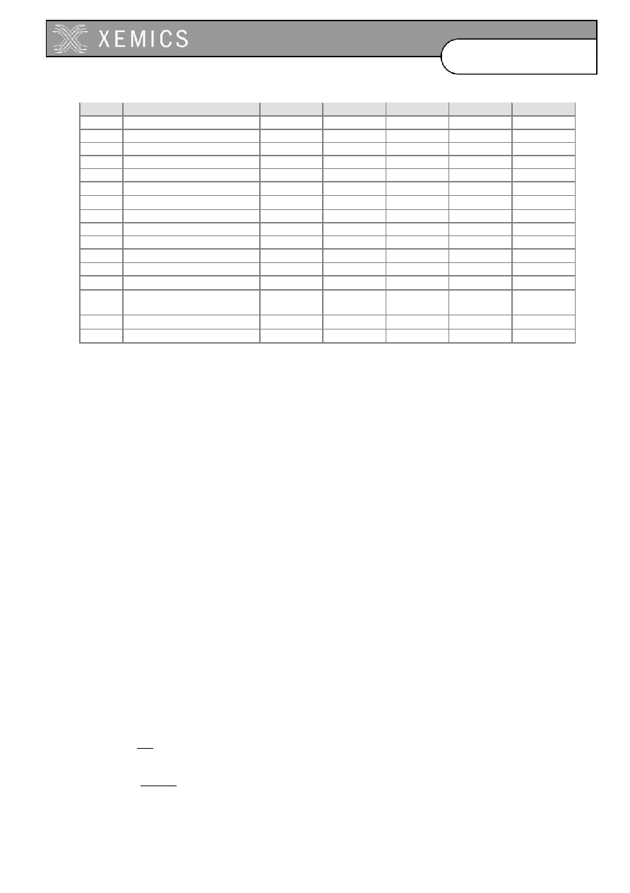
18-8
D0304-40
Datasheet
XE88LC05/05A
sym
description
min
typ
max
unit
Comment
gain
gain at DC
80
100
dB
1
GBW
0
gain bandwidth product
25
70
kHz
6
C
L0
capacitive
load
5 nF
6
GBW
1
gain bandwidth product
250
450
kHz
7
C
L1
capacitive
load
200 pF
7
m
phase margin
55
65
∞
8
R
L
resistive
load
5
k
5
SR slew
rate
10
30
kV/s
9
CMR
common mode input range
VSS-0.2
VBAT-1.2 V
2
OR output
range
VSS+0.2
VBAT-0.2
V
V
off
offset
±
5
mV
CMRR common mode rejection
60
dB
3
noise
integrated input noise
50
100
µ
Vrms
PSRR power supply rejection
ratio
20 60
dB 4
I
quie
quiescent bias current
150
µ
A
I
off
off
current
1
µ
A
1.
For the minimal resistive load and the maximal capacitive load
2.
The amplifier common mode is VSS in the 4-20mA loop.
3. At
DC
4.
At DC. Only a low rejection ratio is needed since the D/A output refers directly to the power supplies.
5.
Short circuit protection at >3mA.
6. GBW when the maximal load is cl0 and with the bit BW=0
7.
GBW when the maximal load is cl1 and with the bit BW=1
8. In both cases BW=0 and BW=1 for the maximal capacitive load and the minimal resistive load.
9.
For maximal load C
L0
, BW=0 and maximal resistive load R
L
Table 18-8. Specification of the amplifier.
18.6 Low pass filter
Several low pass filters are proposed here as examples. Other filter types are possible depending on
the features or constraints of the application.
If the filter is inverting the signal, the bit INV can be used to invert the D/A output. This inversion does
not need to be done by calculation.
A first or second order low pas filter can be built with the amplifier. If higher order filters are needed,
additional first or second order sections can be added using external amplifiers.
18.6.1
First order low pass filter
Figure 18-2 shows a possible implementation of a first order low pass filter. Ideally, the analog ground
should be halfway between VBAT and VSS. The gain G and cut-off frequency f
c
of such a filter are
given by:
C
R
f
R
R
G
c
2
1
2
2
1
=
=

18-9
D0304-40
Datasheet
XE88LC05/05A
As an example, to obtain a 1kHz filter with unity gain, we can choose C=1nF and R1=R2=150k.
XE88LCxx
DAS_OUT
DAS_AI_M
DAS_AO
DAS_AI_P
amp
analog ground
R
1
R
2
D
A
c
o
n
t
r
o
l
C
Figure 18-2. First order low pass filter.
18.6.2
Second order low pass filter
Figure 18-3 shows an example of a second order low pass filter using the multi-feedback architecture.
The gain G, cut-off frequency f
c
and the damping factor (or quality factor Q) as a function of the
factors k and m (see Figure 18-3) are given by:
kmn
RC
f
n
km
n
Q
k
G
c
2
1
2
)
1
(
2
1
=
+
=
=
-
=
For a second order Butterworth filter,
2
2
=
. For smaller damping factors, the filter is under
damped resulting in overshoots on the step response. For higher damping factors, the filter is over
damped resulting in a smooth but slower step response.
An example of a 1dB ripple Chebychev filter with a cut-off frequency of about 1.5kHz and a DC gain of
1 is given by choosing m=0.22, k=1, n=0.5, R=330k and C=1nF. The resistor nR can be rounded to
180k.
A 60Hz unity gain low pass Butterworth filter can be built choosing R=180k, C=12nF, k=1, m=0.183,
n=8.33.
Note that parasitic capacitors between the DAS_OUT node and the filter output DAS_AO will
adversely affect the high frequency behavior of the filter. Care should be taken when routing these
signals.

18-10
D0304-40
Datasheet
XE88LC05/05A
XE88LCxx
DAS_OUT
DAS_AI_M
DAS_AO
DAS_AI_P
amp
analog ground
R C
nR
mC kR
D
A
c
o
n
t
r
o
l
Figure 18-3. Second order low pass filter.
18.7 4-20mA
loop
18.7.1
2-wire loop with first order filtering
The amplifier can be used to build a 4-20mA loop externally. Figure 18-4 shows the principle of such
a 2-wire loop using a first order low pass filter.
In a 2-wire loop, the current consumption of the sensor and read-out electronics is drawn on the same
wires as the signal current. The current consumption of the sensor and read-out electronics should
therefore remain below 4mA. The signal current is then added by the bipolar transistor. The resistors
R
lim1
and R
lim2
are added to protect the bipolar transistor against high transient currents during power-
up. R
lim1
is generally set to a few k. The value of R
lim2
is chosen as a function of the external loop
voltage V
EXT
and the transistor saturation voltage V
CEsat
.
mA
mA
R
V
V
R
sense
CEsat
EXT
20
)
20
(
2
lim
-
-
=
If V
EXT
is larger than 5.5V, a voltage regulator has to be inserted. Since the quiescent current of the
regulator adds up to the 4mA budget, a component with sufficiently low quiescent current has to be
selected.
The resistor R
sense
measures the total current in the loop (if R
sense
<<R
f2
). The resistors R
f1
and R
f2
are
used to set the gain and R
f2
and C
f
to set the bandwidth of the filter. The resistor R
offset
adds an offset
to the filter voltage so that the code 0 of the D/A corresponds to 4mA. The amplifier will force a current
through the bipolar transistor so that the voltage on the filter V
f
and VSS on R
sense
is equal. This
transforms the filter voltage into a loop current I
loop
=(VSS-V
EXT
-)/R
sense
.

18-11
D0304-40
Datasheet
XE88LC05/05A
The resistor value R
sense
is generally chosen between 50 and 150 resulting in a 1V to 3V voltage
drop at maximal loop current. The resistor R
f2
is then chosen much larger depending on the current
error requirement. Allowing for an error of 0.1% gives R
f2
=R
sense
/0.001.
The resistor R
offset
may be omitted but it will reduce the useful code range of the D/A.
Using the large bandwidth of the amplifier is recommended since this increases the rejection of supply
current variations of the other components in the loop. A bypass capacitor between VBAT and VSS
will also reduce the high frequency current variations. Values will depend on the voltage regulator
used. The software in the XE88LC05 should keep the current supply of the circuit as stable as
possible. This means that the clock frequency should kept constant, peripherals should not be
switched on and off, the current in the sensor is kept constant, the processor should not use the halt
or sleep modes, etc.
XE88LCxx VBAT
DAS_OUT
DAS_AI_P
DAS_AO
DAS_AI_M
VSS
D
A
c
o
n
t
r
o
l
amp
4-20mA
R
sense
R
f1
R
f2
C
f
R
lim1
R
lim2
Voltage
regulator
4-20mA
R
offset
Sensor
V
EXT
+
V
EXT
-
V
f
VSS
VBAT
Figure 18-4. 2-wire 4-20mA loop with first order filter
The resistor R
f1
can then be calculated to set the full scale D/A code range (depends on the PWM
modulation m, see section 18.4.3.2) equal to the full scale signal current of 16mA:
mA
R
R
VSS
VBAT
R
sense
m
f
m
f
16
2
)
1
2
(
)
(
2
1
-
-
The resistor R
offset
can be calculated in order to obtain a 4mA current while the D/A code is 0:
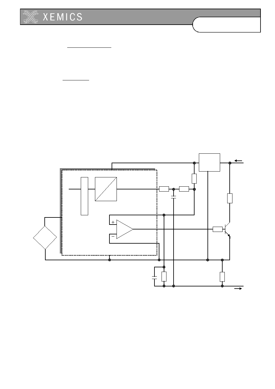
18-12
D0304-40
Datasheet
XE88LC05/05A
mA
R
R
VSS
VBAT
R
sense
f
offset
4
)
(
2
-
The capacitor C
f
can be calculated from the first order filter cut-off frequency f
c
:
2
1
2
1
2
f
f
c
f
f
f
R
R
f
R
R
C
+
=
As an example, for VBAT-VSS=5V, m=4, R
sense
=50, V
EXT
=30V and a 1kHz low pass filter, we can
use:
R
lim1
=1k, R
lim2
=1k, R
f1
=560k, R
f2
=100k, R
offset
=2.4M, C
f
=1.8nF.
18.7.2
2-wire loop with second order filtering
A second order filter function can be implemented by replacing the resistor R
f1
in Figure 18-4 by
another first order filter section as shown in Figure 18-5. The value of R
f1a
+R
f2a
has to be chosen the
same way as R
f1
in the first order schematic.
XE88LCxx VBAT
DAS_OUT
DAS_AI_P
DAS_AO
DAS_AI_M
VSS
D
A
c
o
n
t
r
o
l
amp
4-20mA
R
sense
R
f1a
R
f2
C
f2
R
lim1
R
lim2
Voltage
regulator
4-20mA
R
offset
Sensor
V
EXT
+
V
EXT
-
V
f
VSS
VBAT
R
f1b
C
f1
Figure 18-5. 2-wire 4-20mA loop with second order filtering.
Another possibility is shown in Figure 18-6. The advantage this solution is that it is easier to stabilize
depending on the component parasitics and board layout. But since it limits the bandwidth of the
current regulation loop, it reduces the rejection of the supply current variations.
For this schematic, all the equations of the first order schematic remain valid. The values of R
fs
and
C
fs
can be calculated from the cut-off frequency:
18-13
D0304-40
Datasheet
XE88LC05/05A
c
fs
fs
f
C
R
2
1
=
For the 1kHz example, we can chose R
fs
=150k and C
fs
=1nF (set BW=0 in this case).
XE88LCxx VBAT
DAS_OUT
DAS_AI_P
DAS_AO
DAS_AI_M
VSS
D
A
c
o
n
t
r
o
l
amp
4-20mA
R
sense
R
f2
C
f
R
lim1
R
lim2
Voltage
regulator
4-20mA
R
offset
Sensor
V
EXT
+
V
EXT
-
V
f
VSS
VBAT
R
f1
R
fs
C
fs
Figure 18-6. 2-wire 4-20mA with second order filter and increased stability

19-1
dab_ff - 1.0 ≠ 17 october 2002
D0304-40
Datasheet
XE88LC05/05A
19. Bias D/A (DAB)
19.1
Features
19-2
19.2
General description
19-2
19.3
Register map
19-2
19.4
D/A specification
19-3
19.5
Amplifier specification
19-3
19.6
Application examples
19-4
19.6.1
Voltage controlled sensor bias
19-4
19.6.2
Current controlled sensor bias
19-5

19-2
D0304-40
Datasheet
XE88LC05/05A
19.1 Features
∑
8 bit low frequency A/D
∑
On-chip
amplifier
∑
Current and voltage controlled applications can be implemented
19.2 General
description
DAB_R_P
DAB_OUT
DAB_R_M
DAB_AIP
DAB_AOP
DAB_AOM
DAB_AI_M
D
A
c
o
n
t
r
o
l
amp
Figure 19-1. General block diagram
Figure 19-1 shows the general block diagram of the D/A peripheral. It consists of a control block that
manages all communication with the CPU and sets the configuration of the peripheral. The D/A
converts the digital data in an analog output signal. An amplifier is added that can be used to drive the
large sensor currents.
19.3 Register
map
The bias D/A has two registers.
Pos. RegDabIn
rw
reset
function
7-0 DabIn(7:0)
rw 0
resetsystem
Data to convert
Table 19-1. RegDabIn
Pos. RegDabCfg
rw
reset
function
7-2
r 0
Unused
1-0 Enable(1:0)
rw 00
resetsystem
bit 1: enables the amplifier when 1
bit 0: enables the D/A when 1
Table 19-2. RegDabCfg

19-3
D0304-40
Datasheet
XE88LC05/05A
19.4 D/A
specification
The D/A generates a voltage on node DAB_OUT that is proportional to the code RegDabIn in
between the positive reference voltage DAB_R_P and the negative reference voltage DAB_R_M. The
voltage on DAB_R_P always has to be larger than the voltage on DAB_R_M. The D/A is intended for
very low frequency use. The specification is given in Table 19-3. Larger than 100pF capacitors are
allowed on the node DAB_OUT, but the step response will increase proportionally.
sym
description
min
typ
max
unit
note
wda
number of input bits
8
bits
tstep step
response
0.25
1
ms 1
OR
D/A output range
DAB_R_M
DAB_R_P
refp DAB_R_P
range
VSS+2.3
VBAT V
refn DAB_R_M
range
VSS
VBAT-2.3
V
1. Time to reach the final value within 5%, C
L
on DAB_OUT smaller than 100pF.
Table 19-3. D/A specification.
19.5 Amplifier
specification
The amplifier output stage is a single transistor follower that is able to drive large currents. This
transistor is not connected internally so that different circuit configurations are possible (see next
section). In order to guarantee correct functionality, the voltage on the output pins has to respect the
specifications VR
AOP
and VR
AOM
as indicated in Table 19-4.
sym
description
min
typ
max
unit
Note
gain
gain at DC
60
90
dB
1
GBW
gain bandwidth product
100
4500
Hz
1
m
phase margin
60
80
∞
1
R
L
resistive
load
300
100000
C
L
capacitive
load
1
nF
CMR
common mode input range
VSS
VBAT
V
VR
AOM
DAB_AOM voltage range
VSS+0.2
DAB_AOP-0.2 V
1
VR
AOP
DAB_AOP voltage range
VSS+2.3
VBAT
V
1
V
off
offset
±
10
mV
noise
integrated input noise
60
100
µ
Vrm
s
I
source
max source current
10
40
mA
PSRR power supply rejection ratio
80
dB
2
I
bias
quiescent bias current
5
10
µ
A
I
off
off
current
0.1
1
µ
A
1. For all possible combinations of resistive load and capacitive load.
2. At
DC.
Table 19-4. Amplifier specification.

19-4
D0304-40
Datasheet
XE88LC05/05A
19.6 Application
examples
19.6.1
Voltage controlled sensor bias
Figure 19-2 shows the basic connectivity to have a voltage controlled sensor bias. The D/A will
generate a voltage between vrep and vrefn proportional to the input code. The amplifier will copy the
D/A voltage to the sensor. The D/A code can be used to do a software temperature calibration of the
sensor for instance.
Filter capacitors can be added in parallel with the sensor reference and signal, on V
refp
, V
refn
and
DAB_OUT.
The voltages V
refp
and V
refn
can be filtered before being connected to the D/A reference inputs. The
reference voltages can be connected directly to VBAT and VSS for simplicity. They can also be
connected to VBAT and VSS through a low pass filter that rejects the high frequency supply noise.
Finally, in most cases, the voltage range of interest for the voltage V
sensor
on the sensor is only a
fraction of the supply voltage. By generating V
refp
and V
refn
equal to the limits of the voltage range of
interest, the resolution of the D/A can be increased. Example: if a supply of 5V is used and the
reference voltage is equal to the supply, the D/A can generate a sensor voltage between 0V and 5V in
steps of about 5V/25520mV. If the sensor voltage is always to be between 3V and 4V, and by
connecting V
refn
=3V and V
refp
=4V, the sensor voltage is adjustable between 3V and 4V with steps of
about 1V/2554mV.
XE88LCxx
DAB_R_P
DAB_R_M
DAB_OUT
DAB_AIM
DAB_AOP
DAB_AOM
DAB_AIP
D
A
amp
signal
reference
VBAT
VSS
V
sensor
V
refp
V
refn
Figure 19-2. Voltage controlled bridge bias principle.
Note that the voltage on the sensor can not be higher than VBAT-0.2V in the example of Figure 19-2
(specification VR
AOM
in Table 19-4).
19-5
D0304-40
Datasheet
XE88LC05/05A
19.6.2
Current controlled sensor bias
Figure 19-3 shows the principle of a current controlled sensor bias schematic. In this case, the
amplifier forces the voltage V
R
to be equal to the D/A output voltage V
D/A
. The current I
sensor
through
the sensor is given by:
sense
refn
refp
sense
A
D
refp
sense
R
refp
sensor
R
code
V
V
R
V
V
R
V
V
I
)
255
1
(
)
(
/
-
-
=
-
=
-
=
The voltage V
sensor
can be calculated as a function of the current I
sensor
and the sensor impedance.
Note that the voltage V
R
>VSS+2.3V and V
R
-V
sensor
>0.2V (VR
AOP
and VR
AOM
specifications in Table
19-4) to guarantee correct functionality of this schematic.
Choosing the V
refp
equal to the supply voltage or close to the supply voltage in order to have the
highest possible voltage on the sensor is recommended. From the equation, it can be seen that the
sensor current step per LSB can be made smaller by reducing the voltage between V
refp
and V
refn
or
by increasing the sense resistor value.
As for the voltage controlled sensor bias, capacitors can be added on several nodes to filter out the
noise.
XE88LCxx
DAB_R_P
DAB_R_M
DAB_OUT
DAB_AIP
DAB_AOP
DAB_AOM
DAB_AIM
D
A
amp
signal
reference
V
refp
V
refn
R
sense
V
sensor
V
D/A
V
R
VSS
Figure 19-3. Current controlled bridge bias
In Figure 19-4, the sense resistor is inserted between the negative reference voltage and the sensor.
This schematic has the same principle as above, but it is easier to respect the limits on VR
AOP
when
VBAT is low. The sensor current is now:
sense
refn
refp
sense
refn
A
D
sense
refn
R
sensor
R
code
V
V
R
V
V
R
V
V
I
)
255
(
)
(
/
-
=
-
=
-
=
19-6
D0304-40
Datasheet
XE88LC05/05A
In this case, it is recommended to choose V
refn
equal to VSS or close to VSS in order to have the
highest possible voltage on the sensor. The only limit is now V
sensor
<VBAT-0.2V.
XE88LCxx
DAB_R_P
DAB_R_M
DAB_OUT
DAB_AIM
DAB_AOP
DAB_AOM
DAB_AIP
D
A
amp
V
refp
V
refn
V
D/A
signal
reference
R
sense
V
sensor
V
R
VBAT
Figure 19-4. Current controlled sensor bias.
.

20-1
cnt_ff - 1.2 ≠ 14 march 2002
D0304-40
Datasheet
XE88LC05/05A
20. Counters/Timers/PWM
20.1
Features
20-2
20.2
Overview
20-2
20.3
Register map
20-2
20.4
Interrupts and events map
20-3
20.5
Block schematic
20-4
20.6
General counter registers operation
20-4
20.7
Clock selection
20-5
20.8
Counter mode selection
20-5
20.9
Counter / Timer mode
20-6
20.10
PWM mode
20-8
20.11
Capture function
20-9
20-2
D0304-40
Datasheet
XE88LC05/05A
20.1 Features
∑
4 x 8-bits timer/counter modules or 2 x 16-bits timers/counter modules
∑
Each with 4 possible clock sources
∑
Up/down counter modes
∑
Interrupt and event generation
∑
Capture function (internal or external source)
∑
Rising, falling or both edge of capture signal
∑
PA[3:0] can be used as clock inputs (debounced or direct)
∑
2 x 8 bits PWM or 2 x 16 bits PWM
∑
PWM resolution of 8, 10, 12, 14 or 16 bits
∑
Complex mode combinations are possible between counter, capture and PWM modes
20.2 Overview
CounterA and CounterB are 8-bit counters and can be combined to form a 16-bit counter. CounterC
and CounterD exhibit the same features.
The counters can also be used to generate two PWM outputs on PB[0] and PB[1]. In PWM mode one
can generate PWM functions with 8, 10, 12, 14 or 16 bit wide counters.
The counters A and B can be captured by events on an internal or an external signal. The capture can
be performed on both 8-bit counters running individually on two different clock sources or on both
counters chained to form a 16-bit counter. In any case, the same capture signal is used for both
counters.
When the counters A and B are not chained, they can be used in several configurations: A and B as
counters, A and B as captured counters, A as PWM and B as counter, A as PWM and B as captured
counter.
When the counters C and D are not chained, they can be used either both as counters or counter C
as PWM and counter D as counter.
20.3 Register map
Bit
RegCntA
rw
reset
function
7-0 CounterA r
xxxxxxxx
8-bits counter value
7-0 CounterA w
xxxxxxxx 8-bits
comparison value
Table 20-1. RegCntA
bit
RegCntB
rw
reset
function
7-0 CounterB r
xxxxxxxx
8-bits counter value
7-0 CounterB w
xxxxxxxx 8-bits
comparison value
Table 20-2. RegCntB
Note: When writing to RegCntA or RegCntB, the processor writes the counter comparison values.
When reading these locations, the processor reads back either the actual counter value or the last
captured value if the capture mode is active.
bit
RegCntC
rw
reset
function
7-0 CounterC r
xxxxxxxx
8-bits counter value
7-0 CounterC w
xxxxxxxx 8-bits
comparison value
Table 20-3. RegCntC
20-3
D0304-40
Datasheet
XE88LC05/05A
bit
RegCntD
rw
reset
function
7-0 CounterD r
xxxxxxxx
8-bits counter value
7-0 CounterD w
xxxxxxxx 8-bits
comparison value
Table 20-4. RegCntD
Note: When writing RegCntC or RegCntD, the processor writes the counter comparison values.
When reading these locations, the processor reads back the actual counter value.
bit
RegCntCtrlCk
rw
reset
function
7-6
CntDCkSel(1:0)
rw
xx
Counter d clock selection
5-4
CntCCkSel(1:0)
rw
xx
Counter c clock selection
3-2
CntBCkSel(1:0)
rw
xx
Counter b clock selection
1-0
CntACkSel(1:0)
rw
xx
Counter a clock selection
Table 20-5. RegCntCtrlCk
bit
RegCntConfig1
rw
Reset
function
7
CntDDownUp
rw
x
Counter d up or down counting (0=down)
6
CntCDownUp
rw
x
Counter c up or down counting (0=down)
5
CntBDownUp
rw
x
Counter b up or down counting (0=down)
4
CntADownUp
rw
x
Counter a up or down counting (0=down)
3
CascadeCD
rw
x
Cascade counter c & d (1=cascade)
2
CascadeAB
rw
x
Cascade counter a & b (1=cascade)
1 CntPWM1 rw
0
resetsystem
Activate pwm1 on counter c or c+d (PB(1))
0 CntPWM0 rw
0
resetsystem
Activate pwm0 on counter a or a+b (PB(0))
Table 20-6. RegCntConfig1
bit
RegCntConfig2
rw
Reset
function
7-6
CapSel(1:0)
rw
00 resetsystem
Capture source selection
5-4
CapFunc(1:0)
rw
00 resetsystem
Capture function
3-2
Pwm1Size(1:0)
rw
xx
Pwm1 size selection
1-0
Pwm0Size(1:0)
rw
xx
Pwm0 size selection
Table 20-7. RegCntConfig2
bit
RegCntOn
rw
Reset
Function
7-4 -- r 0000
Reserved
3
CntDEnable
rw
0 resetsystem
Enable counter d
2
CntCEnable
rw
0 resetsystem
Enable counter c
1
CntBEnable
rw
0 resetsystem
Enable counter b
0
CntAEnable
rw
0 resetsystem
Enable counter a
Table 20-8. RegCntOn
20.4 Interrupts and events map
Interrupt source
Mapping in the
interrupt manager
Mapping in the event
manager
IrqA RegIrqHigh(4) RegEvn(7)
IrqB RegIrqLow(5) RegEvn(3)
IrqC RegIrqHigh(3) RegEvn(6)
IrqD RegIrqLow(4) RegEvn(2)
Table 20-9. Interrupt and event mapping.
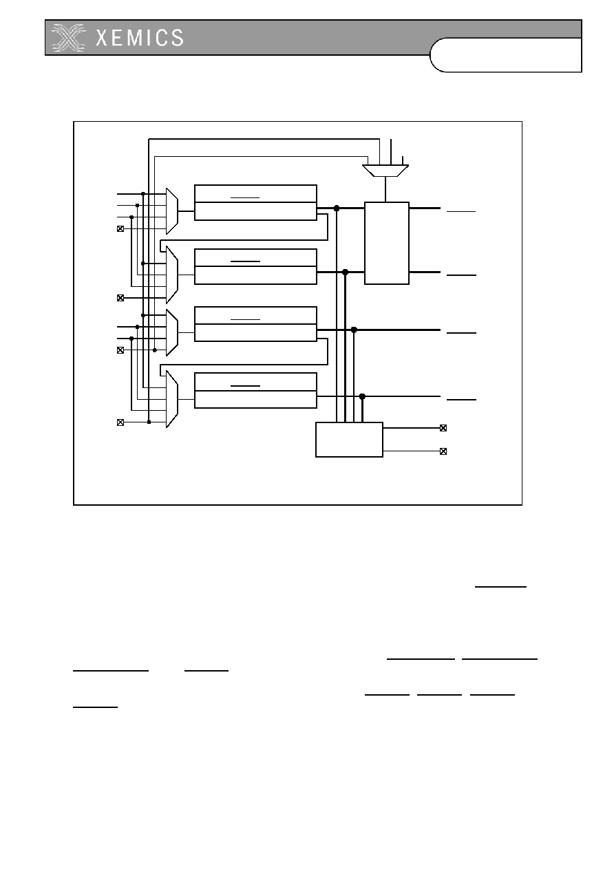
20-4
D0304-40
Datasheet
XE88LC05/05A
20.5 Block
schematic
PB(0)
Capture
ck32k
ck1k
PA(0)
RegCntA (write)
Counter A
PA(2)
RegCntC (write)
Counter C
RegCntD (write)
Counter D
RegCntB (write)
Counter B
PA(1)
PA(3)
ck128
ckrcext/4
ckrcext
ck1k
ck32k
PWM
PB(1)
RegCntA (read)
RegCntB (read)
RegCntC (read)
RegCntD (read)
Figure 20-1: Counters/timers block schematic
20.6
General counter registers operation
Counters are enabled by CntAEnable, CntBEnable, CntCEnable, and CntDEnable in RegCntOn.
To stop the counter X, CntXEnable must be reset. To start the counter X, CntXEnable must be set.
When counters are cascaded, CntAEnable and CntCEnable also control respectively the counters B
and D.
In the control registers, all registers must be written in this order: RegCntCtrlCk, RegCntConfig1,
RegCntConfig2 and all RegCntX because several bits have no default values at reset.
All counters have a corresponding 8-bit read/write register: RegCntA, RegCntB, RegCntC, and
RegCntD. When read, these registers contain the counter value (or the captured counter value).
When written, they modify the counter comparison values.
For a correct acquisition of the counter value, use one of the three following methods:
1) Stop the concerned counter, perform the read operation and restart the counter. While
stopped, the counter content is frozen and the counter does not take into account the clock
edges delivered on the external pin.
20-5
D0304-40
Datasheet
XE88LC05/05A
2) For slow operating counters (typically at least 8 times slower than the CPU clock),
oversample the counter content and perform a majority operation on the consecutive read
results to select the correct actual content of the counter.
3) Use the capture mechanism.
When a value is written into the counter register while the counter is in counter mode, both the
comparison value is updated and the counter value is modified. In upcount mode, the register value is
reset to zero. In downcount mode, the comparison value is loaded into the counter. Due to the
synchronization mechanism between the processor clock domain and the external clock source
domain, this modification of the counter value can be postponed until the counter is enabled and it
receives it's first valid clock edge.
In the PWM mode, the counter value is not modified by the write operation in the counter register.
Changing the counter mode, does not update the counter value (no load in downcount mode).
20.7 Clock
selection
The clock source for each counter can be individually selected by writing the appropriate value in the
register RegCntCtrlCk.
Table 20-10 gives the correspondence between the binary codes used for the configuration bits
CntACkSel(1:0), CntBCkSel(1:0), CntCCkSel(1:0) or CntDCkSel(1:0) and the clock source
selected respectively for the counters A, B, C or D.
Clock source for
CntXCkSel(1:0)
CounterA
CounterB
CounterC
CounterD
11 Ck128
10 CkRc/4
Ck1k
01 CkRc
Ck32k
00 PA(0)
PA(1)
PA(2)
PA(3)
Table 20-10: Clock sources for counters A, B, C and D
The CkRc clock is the RC oscillator. The clocks below 32kHz can be derived from the RC oscillator or
the crystal oscillator (see the documentation of the clock block). A separate external clock source can
be delivered on Port A for each individual counter.
The external clock sources can be debounced or not by setting the Port A configuration registers.
The clock source can be changed only when the counter is stopped.
20.8 Counter mode selection
Each counter can work in one of the following modes:
1) Counter, downcount & upcount
2) Captured counter, downcount & upcount (only counters A&B)
3) PWM, downcount
The counters A and B or C and D can be cascaded or not. In cascaded mode, A and C are the LSB
counters while B and D are the MSB counters.
Table 20-11 shows the different operation modes of the counters A and B as a function of the mode
control bits. For all counter modes, the source of the down or upcount selection is given (either the bit
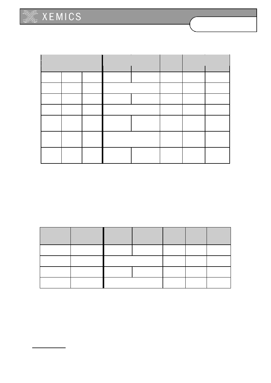
20-6
D0304-40
Datasheet
XE88LC05/05A
CntADownUp or the bit CntBDownUp). Also, the mapping of the interrupt sources IrqA and IrqB and
the PWM output on PB(0) in these different modes is shown.
CascadeAB
CountPWM0
CapFunc(1:0)
Counter A
mode
Counter B
mode
IrqA
source
IrqB
source
PB(0)
function
0 0 00
Counter 8b
Downup: A
Counter 8b
Downup: B
Counter
A
Counter
B
PB(0)
1 0 00
Counter 16b AB
Downup: A
Counter
AB
- PB(0)
0 1 00
PWM 8b
Down
Counter 8b
Down
-
Counter
B
PWM A
1 1 00
PWM 10 ≠ 16b AB
Down
- -
PWM
AB
0 0
1x
or
x1
Captured
counter 8b
Downup: A
Captured
counter 8b
Downup: B
Capture
A
Capture
B
PB(0)
1 0
1x
or
x1
Captured counter 16b AB
Downup: A
Capture
AB
Capture
AB
PB(0)
0 1
1x
or
x1
PWM 8b
Down
Captured
counter 8b
Downup: B
Must not
be used
Capture
B
PWM A
Table 20-11: Operating modes of the counters A and B
Table 20-12 shows the different operation modes of the counters C and D as a function of the mode
control bits. For all counter modes, the source of the down or upcount selection is given (either the bit
CntCDownUp or the bit CntDDownUp). The mapping of the interrupt sources IrqC and IrqD and the
PWM output on PB(1) in these different modes is also shown.
The switching between different modes must be done while the concerned counters are stopped.
While switching capture mode on and off, unwanted interrupts can appear on the interrupt channels
concerned by this mode change.
CascadeCD CountPWM1
Counter C
mode
Counter D
mode
IrqC
Source
IrqD
source
PB(1)
function
0 0
Counter 8b
Downup: C
Counter 8b
Downup: D
Counter
C
Counter
D
PB(1)
1 0
Counter 16b CD
Downup: C
Counter
CD
- PB(1)
0 1
PWM 8b
Down
Counter 8b
Down
- Counter
D
PWM C
1 1
PWM 10 ≠ 16b CD
Down
- -
PWM
CD
Table 20-12: Operating modes of the counters C and D
20.9 Counter / Timer mode
The counters in counter / timer mode are generally used to generate interrupts after a predefined
number of clock periods applied on the counter clock input.
Each counter can be set individually either in upcount mode by setting CntXDownUp in the register
RegCntConfig1 or in downcount mode by resetting this bit. Counters A and B can be cascaded to
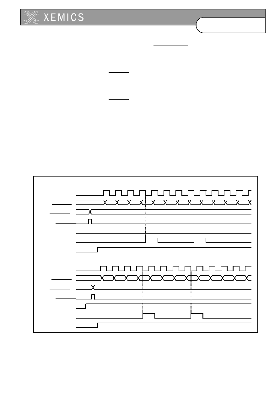
20-7
D0304-40
Datasheet
XE88LC05/05A
behave as a 16 bit counter by setting CascadeAB in the RegCntConfig1 register. Counters C and D
can be cascaded by setting CascadeCD. When cascaded, the up/down count modes of the counters
B and D are defined respectively by the up/down count modes set for the counters A and C.
When in upcount mode, the counter will start incrementing from zero up to the target value which has
been written in the corresponding RegCntX register(s). When the counter content is equal to the
target value, an interrupt is generated at the next falling edge of counter clock. Then the counter is
loaded again with the zero value at the next rising edge of counter clock (Figure 20-2).
When in downcount mode, the counter will start decrementing from the initial load value which has
been written in the corresponding RegCntX register(s) down to the zero value. Once the counter
content is equal to zero, an interrupt is generated at the next falling edge of counter clock. Then the
counter is loaded again with the load value at the next rising edge of counter clock (Figure 20-2).
Be careful to select the counter mode (no capture, not PWM, specify cascaded or not and up or down
counting mode) before writing any target or load value to the RegCntX register(s). This ensures that
the counter will start from the correct initial value. When counters are cascaded, both counter
registers must be written to ensure that both cascaded counters will start from the correct initial
values.
The stopping and consecutive starting of a counter in counter mode without a target or load value
write operation in between can generate an interrupt if this counter has been stopped at the zero
value (downcount) or at it's target value (upcount). This interrupt is additional to the interrupt which
has already been generated when the counter reached the zero or the target value.
down counting
clock counter X
RegcntX_r
XX
3
2
1
0
3
2
1
0
3
2
1
0
RegCntX_w
XX
3
write RegCntX
CntXDownUp
IrqX
CntXEnable
up counting
clock counter X
RegCntX_r
XX
0
1
2
3
0
1
2
3
0
1
2
3
RegCntX_w
XX
3
write RegCntX
CntXDownUp
IrqX
CntXEnable
Figure 20-2. Up and down count interrupt generation.
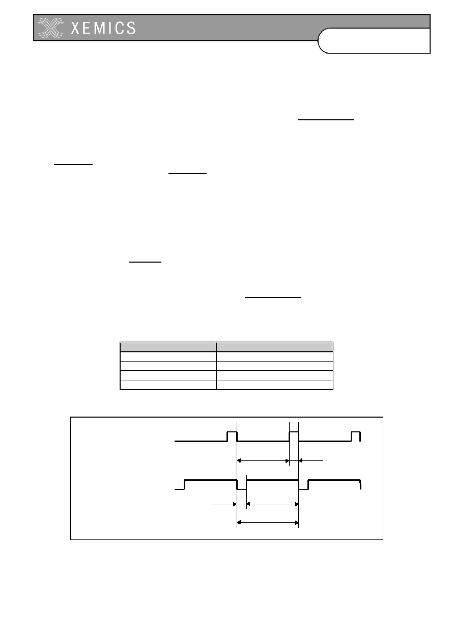
20-8
D0304-40
Datasheet
XE88LC05/05A
20.10 PWM mode
The counters can generate PWM signals (Pulse Width Modulation) on the Port B outputs PB(0) and
PB(1).
The PWM mode is selected by setting CntPWM1 and CntPWM0 in the RegCntConfig1 register. See
Table 20-11 and Table 20-12 for an exact description of how the setting of CntPWM1 and CntPWM0
affects the operating mode of the counters A, B, C and D according to the other configuration settings.
When CntPWM0 is enabled, the PWMA or PWMAB output value overrides the value set in bit 0 of
RegPBOut in the Port B peripheral. When CntPWM1 is enabled, the PWMC or PWMCD output value
overrides the value set in bit 1 of RegPBOut. The corresponding ports (0 and/or 1) of Port B must be
set in digital mode and as output and either open drain or not and pull up or not through a proper
setting of the control registers of the Port B.
Counters in PWM mode always count down, the CntXDownUp bit setting must be reset. No
interrupts and events are generated by the counters which are in PWM mode. Counters do count
circularly: they restart at the maximal value (either 0xFF when not cascaded or 0xFFFF when
cascaded) when respectively an underflow condition occurs in the counting.
The internal PWM signals are low as long as the counter contents are higher than the PWM code
values written in the RegCntX registers. They are high when the counter contents are smaller or
equal to these PWM code values.
The PWM resolution is always 8 bits when the counters used for the PWM signal generation are not
cascaded. PWM0Size(1:0) and PWM1Size(1:0) in the RegCntConfig2 register are used to set the
PWM resolution for the counters A and B or C and D respectively when they are in cascaded mode.
The different possible resolutions in cascaded mode are shown in Table 20-13. Choosing a 16 bit
PWM code higher than the maximum value that can be represented by the number of bits chosen for
the resolution, results in a PWM output which is always tied to 1.
PwmXsize(1:0)
Resolution
11 16
bits
10 14
bits
01 12
bits
00 10
bits
Table 20-13: Resolution selection in cascaded PWM mode
Small PWM code
Large PWM code
T
per
T
hlarge
T
llarge
T
hsmall
T
lsmall
Figure 20-3: PWM modulation examples
The period of the PWM signal is given by the formula:
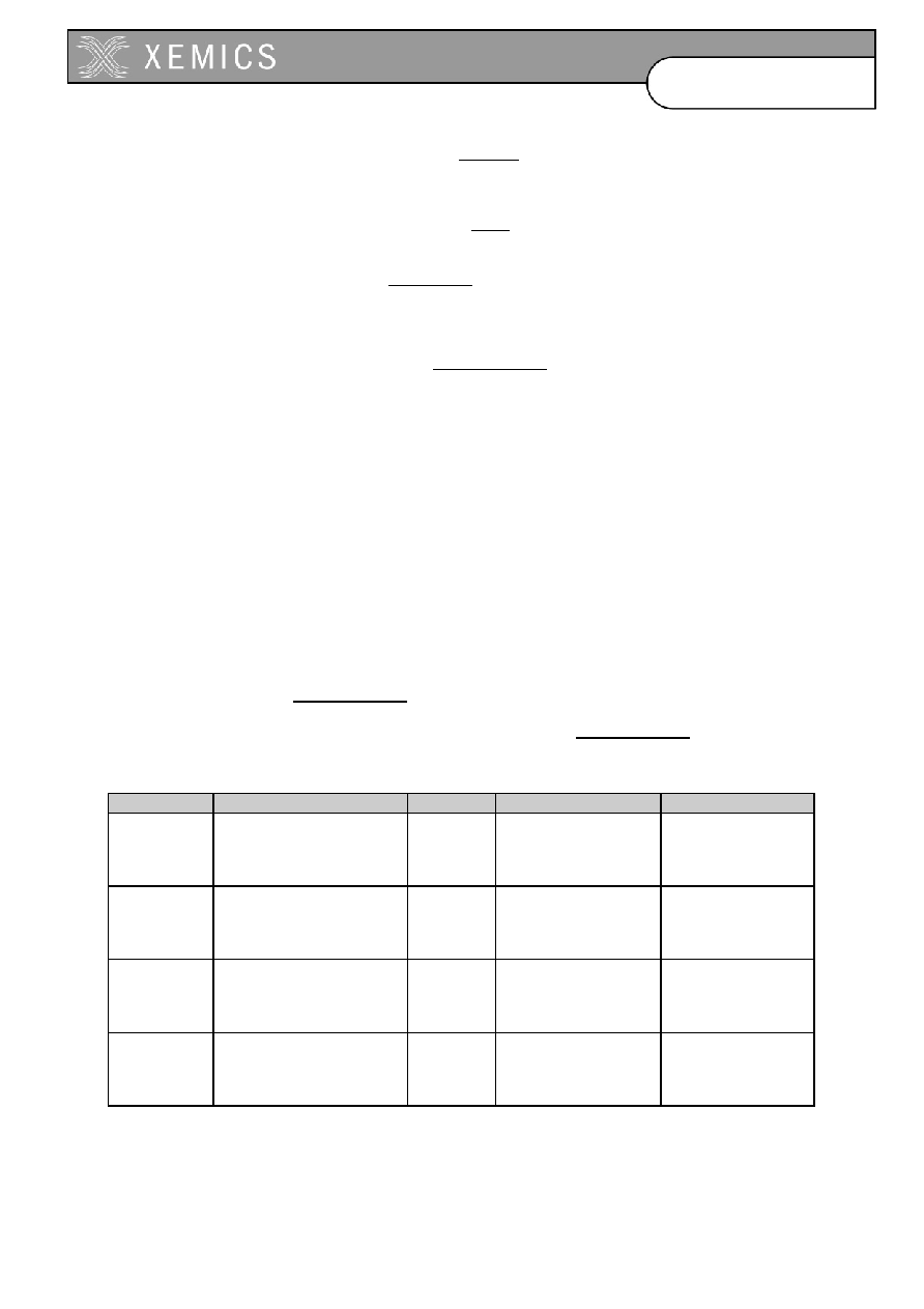
20-9
D0304-40
Datasheet
XE88LC05/05A
ckcnt
resolution
f
Tper
2
=
The duty cycle ratio DCR of the PWM signal is defined as:
Tper
Th
DCR
=
DCR can be selected between 0 % and
100
*
2
1
2
resolution
resolution
-
%.
DCR in % in function of the RegCntX content(s) is given by the relation:
resolution
DCR
2
RegCntX
*
100
=
20.11 Capture function
The 16-bit capture register is provided to facilitate frequency measurements. It provides a safe
reading mechanism for the counters A and B when they are running. When the capture function is
active, the processor does not read anymore the counters A and B directly, but instead reads shadow
registers located in the capture block. An interrupt is generated after a capture condition has been
met when the shadow register content is updated. The capture condition is user defined by selecting
either internal capture signal sources derived from the prescaler or from the external PA(2) or PA(3)
ports. Both counters use the same capture condition.
When the capture function is active, the A and B counters must be written with the value 0xFF and
can either upcount or downcount. They do count circularly: they restart at zero or at the maximal value
(either 0xFF when not cascaded or 0xFFFF when cascaded) when respectively an overflow or an
underflow condition occurs in the counting.
CapFunc(1:0) in register RegCntConfig2 determines if the capture function is enabled or not and
selects which edges of the capture signal source are valid for the capture operation. The source of the
capture signal can be selected by setting CapSel(1:0) in the RegCntConfig2 register. For all
sources, rising, falling or both edge sensitivity can be selected. Table 20-14 shows the capture
condition as a function of the setting of these configuration bits.
CapSel(1:0) Selected capture signal CapFunc
Selected condition
Capture condition
11 1
K
00
01
10
11
Capture disabled
Rising edge
Falling edge
Both edges
-
1 K rising edge
1 K falling edge
1 K both edges
10 32
K
00
01
10
11
Capture disabled
Rising edge
Falling edge
Both edges
-
32 K rising edge
32 K falling edge
32 K both edges
01 PA3
00
01
10
11
Capture disabled
Rising edge
Falling edge
Both edges
-
PA3 rising edge
PA3 falling edge
PA3 both edges
00 PA2
00
01
10
11
Capture disabled
Rising edge
Falling edge
Both edges
-
PA2 rising edge
PA2 falling edge
PA2 both edges
Table 20-14: Capture condition selection

20-10
D0304-40
Datasheet
XE88LC05/05A
CapFunc(1:0) and CapSel(1:0) can be modified only when the counters are stopped otherwise data
may be corrupted during one counter clock cycle.
Due to the synchronization mechanism of the shadow registers and depending on the frequency ratio
between the capture and counter clocks, the interrupts may be generated one or only two counter
clock pulses after the effective capture condition occurred. When the counters A and B are not
cascaded and do not operate on the same clock, the interruptions on IrqA and IrqB which inform that
the capture condition was met, may appear at different moments. In this case, the processor should
read the shadow register associated to a counter only if the interruption related to this counter has
been detected.
It must be noted that when counters A and B are cascaded, the capture might happen at different
cycles for the A and B registers. This is due to the asynchronous relationship between counter and
capture clock and to the fact that the capture condition detection is independent for A and B counters.

21-1
vld_ff - 1.0 ≠ 24 september 2002
D0304-40
Datasheet
XE88LC05/05A
21 VLD (Voltage Level Detector)
21.1
Features
21-2
21.2
Overview
21-2
21.3
Register map
21-2
21.4
Interrupt map
21-2
21.5
VLD operation
21-2

21-2
D0304-40
Datasheet
XE88LC05/05A
21.1 Features
∑
Can be switched off, on or simultaneously with CPU activities
∑
Generates an interrupt if power supply is below a pre-determined level
21.2 Overview
The Voltage Level Detector monitors the state of the system battery. It returns a logical high value (an
interrupt) in the status register if the supplied voltage drops below the user defined level (Vsb).
21.3 Register map
There are two registers in the VLD, namely RegVldCtrl and RegVldStat. Table 221-1 shows the
mapping of control bits and functionality of RegVldCtrl while Table 221-2 describes that for
RegVldStat.
pos.
RegVldCtrl
rw
reset
function
7-4 --
r 0000
reserved
3
VldRange
r w
0 resetsystem
VLD detection voltage range for VldTune = "011":
0 : 1.3V
1 : 2.55V
2-0 VldTune[2:0]
r
w
000
resetsystem
VLD tuning:
000 : +19 %
111 : -18 %
Table 221-1: RegVldCtrl
pos.
RegVldStat
rw
reset
function
7-3 --
r 00000
reserved
2
VldResult
r
0 resetsystem is 1 when battery voltage is below the detection
voltage
1
VldValid
r
0 resetsystem
Indicates when VldResult can be read
0
VldEn
r w
0 resetsystem
VLD enable
Table 221-2: RegVldStat
21.4 Interrupt map
interrupt source
mapping in the interrupt manager
IrqVld RegIrqMid(2)
Table 221-3: Interrupt map
21.5 VLD operation
The VLD is controlled by VldRange, VldTune and VldEn. VldRange selects the voltage range to be
detected, while VldTune is used to fine-tune this voltage level in 8 steps. VldEn is used to enable
(disable) the VLD with a 1(0) value respectively.
Disabled, the block will dissipate no power.

21-3
D0304-40
Datasheet
XE88LC05/05A
symbol
description
min
typ
max
unit
comments
trimming values:
Note 1
VldRange VldTune
1.53
0
000
1.44
0
001
1.36
0
010
1.29
0
011
1.22
0
100
1.16
0
101
1.11
0
110
1.06
0
111
3.06
1
000
2.88
1
001
2.72
1
010
2.57
1
011
2.44
1
100
2.33
1
101
2.22
1
110
Vth Threshold
voltage
2.13
V
1
111
T
EOM
duration of
measurement
2.0
2.5
ms
Note
2
T
PW
Minimum pulse width
detected
875
1350
us
Note
2
Table 221-4: Voltage level detector operation
Note 1: absolute precision of the threshold voltage is
±
10%.
Note 2: this timing is respected in case the internal RC or crystal oscillators are enabled
To start the voltage level detection, the user sets bit VldEn. The measurement is started.
After 2ms, the bit VldValid is set to indicate that the measurement results are valid. From that time
on, as long as the VLD is enabled, a maskable interrupt request is sent if the voltage level falls below
the threshold. One can also poll the VLD and monitor the actual measurement result by reading the
VldResult bit of the RegVldStat. This result is only valid as long as the VldValid bit is `1'.
An interrupt is generated on each rising edge of VldResult.

22-1
LC05 - 1.0 ≠ 17 october 2002
D0304-40
Datasheet
XE88LC05/05A
22 Physical dimensions
CONTENTS
22.1
QFP type package
22-2
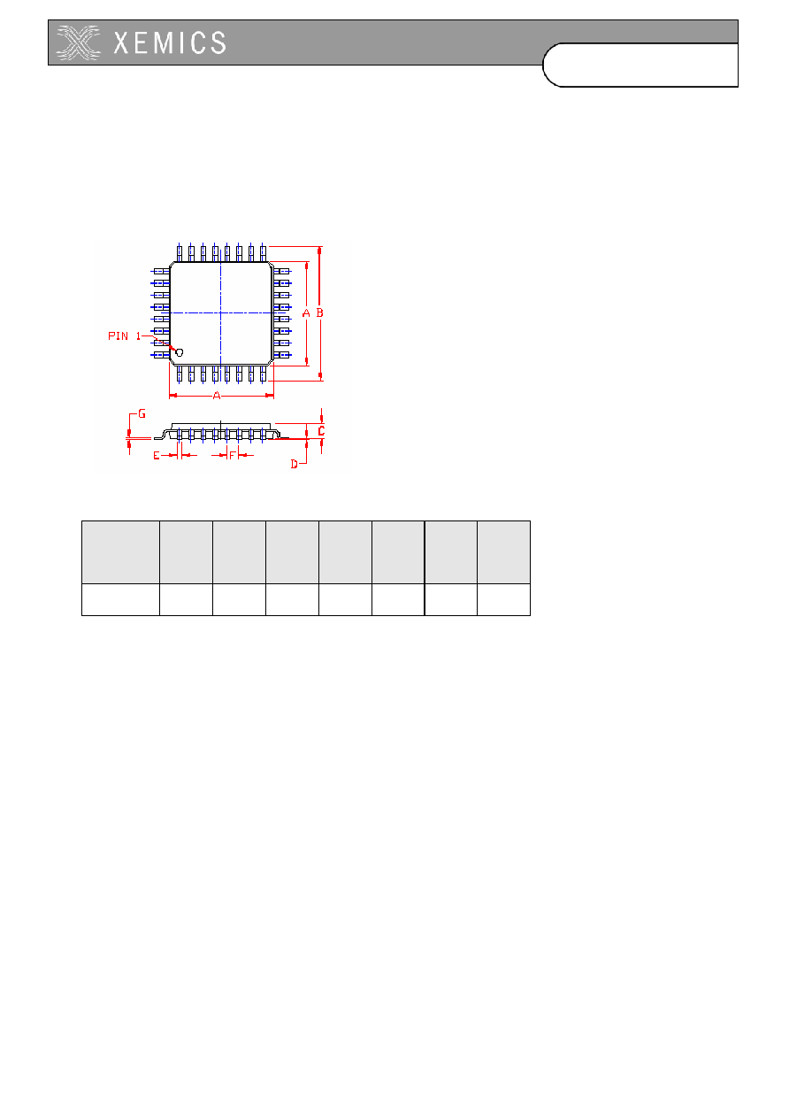
22-2
D0304-40
Datasheet
XE88LC05/05A
22.1 QFP type package
The QFP package dimensions are given in Figure 22-1 and Table 22-1. The dimensions conform to
JEDEC MS-026 Rev. C.
Figure 22-1. QFP type package
package
A
mm
B
mm
C
mm
D
mm
E
mm
F
mm
G
mm
LQFP-64
10.0 12.0 1.4 0.10 0.22 0.5
Table 22-1. QFP package dimensions
XEMICS 2003
All rights reserved. Reproduction in whole or in part is prohibited without the prior written consent of the copyright owner. The information
presented in this document does not form part of any quotation or contract, is believed to be accurate and reliable and may be changed
without notice. No liability will be accepted by the publisher for any consequence of its use. Publication thereof does not convey nor imply
any license under patent or other industrial or intellectual property rights.
XEMICS PRODUCTS ARE NOT DESIGNED, INTENDED, AUTHORIZED OR WARRANTED TO BE SUITABLE FOR USE IN LIFE-
SUPPORT APPLICATIONS, DEVICES OR SYSTEMS OR OTHER CRITICAL APPLICATIONS. INCLUSION OF XEMICS PRODUCTS IN
SUCH APPLICATIONS IS UNDERSTOOD TO BE UNDERTAKEN SOLELY AT THE CUSTOMER'S OWN RISK.
Should a customer purchase or use XEMICS products for any such unauthorized application, the customer shall indemnify and hold
XEMICS and its officers, employees, subsidiaries, affiliates, and distributors harmless against all claims, costs damages and attorney fees
which could arise.