∑ 221 West Industry Court Deer Park, NY 11729-4681 (516) 586-7600 FAX (516) 242-9798 ∑
∑ World Wide Web Site - http://www.sensitron.com ∑ E-Mail Address - sales@sensitron.com ∑
SENSITRON
SEMICONDUCTOR
TECHNICAL DATA
DATA SHEET 639, REV. A
SILICON SCHOTTKY RECTIFIER DIE
Extremely Low Forward Voltage Drop
Applications:
∑ Switching Power Supply ∑ Converters ∑ Free-Wheeling Diodes ∑ Polarity Protection Diode
Features:
∑ Soft Reverse Recovery at Low and High Temperature
∑ Extremely Low Forward Voltage Drop
∑ Low Power Loss, High Efficiency
∑ High Surge Capacity
∑ Guard Ring for Enhanced Durability and Long Term Reliability
∑ Guaranteed Reverse Avalanche Characteristics
∑ Electrically / Mechanically Stable during and after Packaging
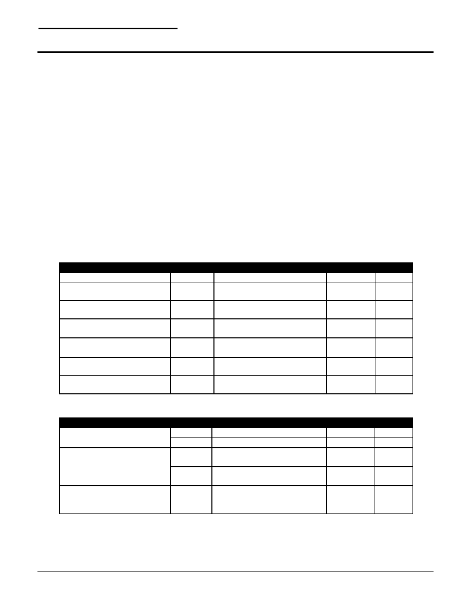
Maximum Ratings
(1)
:
Characteristics
Symbol
Condition
Max.
Units
Peak Inverse Voltage
V
RWM
- 45
V
Max. Average Forward
Current
I
F(AV)
50% duty cycle, rectangular
wave form
15 A
Max. Peak One Cycle Non-
Repetitive Surge Current
I
FSM
8.3 msec, sine pulse
280
A
Non-Repetitive Avalanche
Energy
E
AS
T
J
= 25
∞C, I
AS
= 2.4A
L = 6.5 mH
18.7 mJ
Repetitive Avalanche Current
I
AR
I
AS
decay linearly to 0 in 1
µs
limited by T
J
max V
A
=1.5V
R
2.4 A
Max. Junction Temperature
T
J
-
-55 to +
125
∞C
Max. Storage Temperature
T
stg
-
-55 to +
125
∞C
Electrical Characteristics
(1)
:
Characteristics
Symbol
Condition
Max.
Units
Max. Forward Voltage Drop
V
F1
@ 15 A, Pulse, T
J
= 25
∞C
0.51 V
V
F2
@ 15 A, Pulse, T
J
= 125
∞C
0.47 V
Max. Reverse Current
I
R1
@V
R
= 45V, Pulse,
T
J
= 25
∞C
1.5 mA
I
R2
@V
R
= 45V, Pulse,
T
J
= 125
∞C
250 mA
Max. Junction Capacitance
C
T
@V
R
= 5V, T
C
= 25
∞C
f
SIG
= 1MHz,
V
SIG
= 50mV (p-p)
870 pF
(1) in SHD package
SD125SE45A/B/C
∑ 221 West Industry Court Deer Park, NY 11729-4681 (516) 586-7600 FAX (516) 242-9798 ∑
∑ World Wide Web Site - http://www.sensitron.com ∑ E-Mail Address - sales@sensitron.com ∑
SENSITRON
TECHNICAL DATA
DATA SHEET 639, REV. A
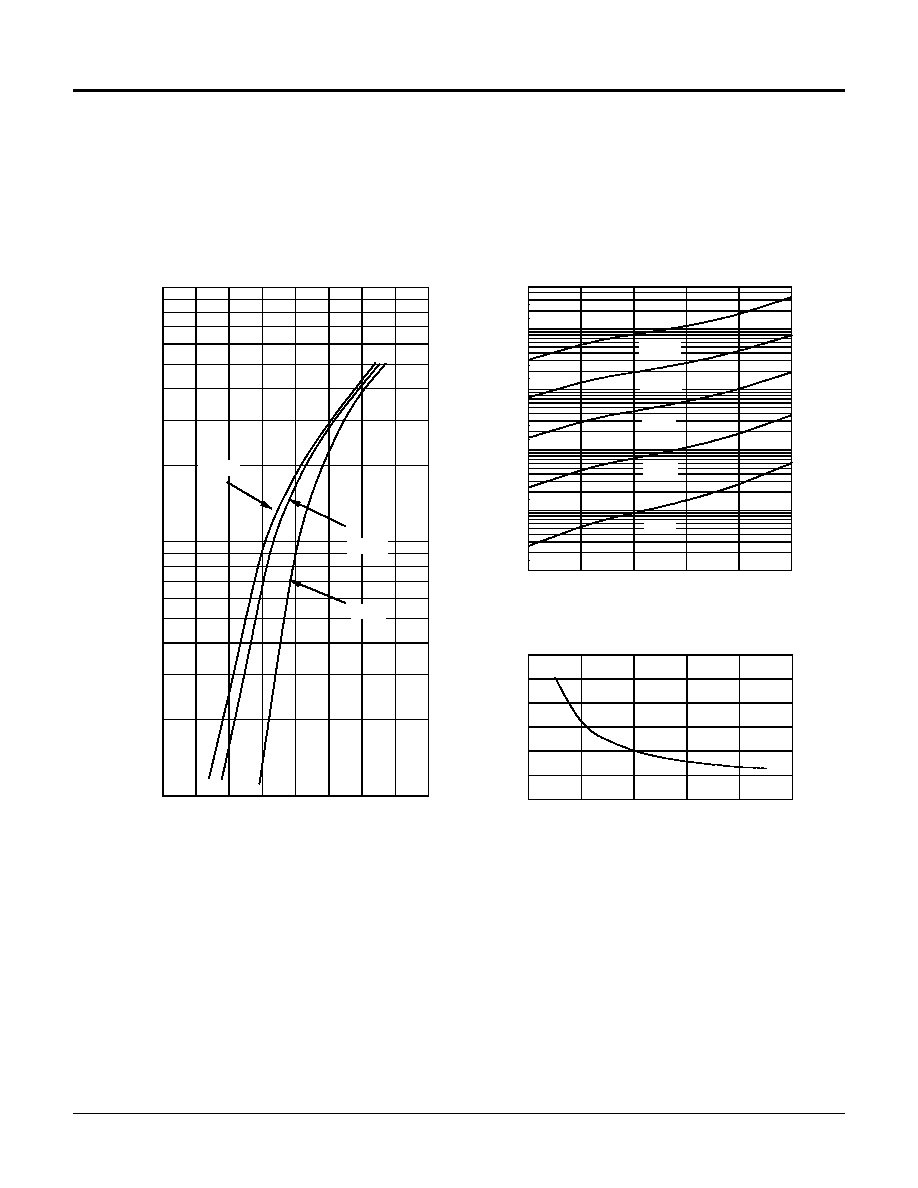
0.0
0.2
0.4
0.6
0.8
Forward Voltage Drop - V
F
(V)
10
0
10
1
10
2
I
n
st
ant
aneous F
o
rward Current
- I
F
(A)
Typical Forward Characteristics
100 ∞C
125 ∞C
25 ∞C
0
10
20
30
40
50
Reverse Voltage - V
R
(V)
10
-2
10
-1
10
0
10
1
10
2
I
n
st
ant
aneous Reverse Current
- I
R
(mA)
Typical Reverse Characteristics
25 ∞C
50 ∞C
75 ∞C
100 ∞C
125 ∞C
0
10
20
30
40
50
Reverse Voltage - V
R
(V)
200
300
400
500
600
700
800
Junct
i
on Capacit
ance - C
T
(pF)
Typical Junction Capacitance
SD125SE45A/B/C
∑ 221 West Industry Court Deer Park, NY 11729-4681 (516) 586-7600 FAX (516) 242-9798 ∑
∑ World Wide Web Site - http://www.sensitron.com ∑ E-Mail Address - sales@sensitron.com ∑
SENSITRON
TECHNICAL DATA
DATA SHEET 639, REV. A
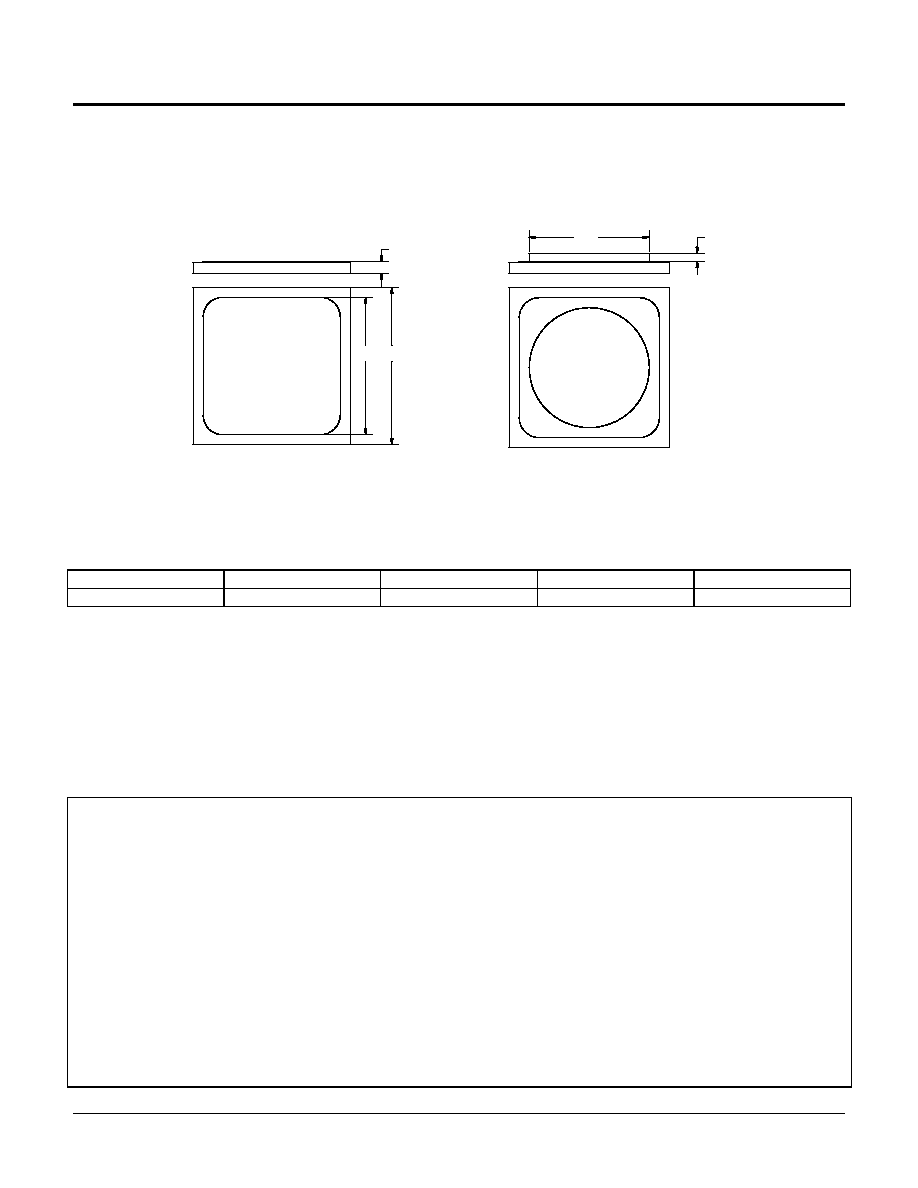
Mechanical Dimensions: In Inches / mm
SD125SE45A/B/C
A B D H h
0.125±0.003 0.116±0.003 0.070±0.005 0.0155±0.001 0.010±0.002
DISCLAIMER:
1- The information given herein, including the specifications and dimensions, is subject to change without prior notice to improve product
characteristics. Before ordering, purchasers are advised to contact the Sensitron Semiconductor sales department for the latest version of the
datasheet(s).
2- In cases where extremely high reliability is required (such as use in nuclear power control, aerospace and aviation, traffic equipment, medical
equipment , and safety equipment) , safety should be ensured by using semiconductor devices that feature assured safety or by means of users'
fail-safe precautions or other arrangement .
3- In no event shall Sensitron Semiconductor be liable for any damages that may result from an accident or any other cause during operation of
the user's units according to the datasheet(s). Sensitron Semiconductor assumes no responsibility for any intellectual property claims or any
other problems that may result from applications of information, products or circuits described in the datasheets.
4- In no event shall Sensitron Semiconductor be liable for any failure in a semiconductor device or any secondary damage resulting from use at
a value exceeding the absolute maximum rating.
5- No license is granted by the datasheet(s) under any patents or other rights of any third party or Sensitron Semiconductor.
6- The datasheet(s) may not be reproduced or duplicated, in any form, in whole or part, without the expressed written permission of Sensitron
Semiconductor.
7- The products (technologies) described in the datasheet(s) are not to be provided to any party whose purpose in their application will hinder
maintenance of international peace and safety nor are they to be applied to that purpose by their direct purchasers or any third party. When
exporting these products (technologies), the necessary procedures are to be taken in accordance with related laws and regulations.
D
h
H
B A
Figure 1
Figure 2
Top side(Anode) metallization:
A = Al - 25 k≈ minimum, Figure 1
B = Ag - 30 k≈ minimum, Figure 1
C = Au - 12 k≈ min, Figure
2
Bottom side (Cathode) metallization:
A, B, C = Ti/Ni/Ag - 30 k≈ minimum.