21
Notice
In the absence of confirmation by device specification sheets,SHARP takes no responsibility for any defects that may occur in equipment using any SHARP devices shown in
catalogs,data books,etc.Contact SHARP in order to obtain the latest device specification sheets before using any SHARP device.
Internet
Internet address for Electronic Components Group http://www.sharp.co.jp/ecg/
LED
Lamp
Super-luminosity(AlGaInP)LED Lamp
GL3Z
t
404B0S series
GL3Z
t
404B0S series
Viewing Angle: 40° (2
1/2) ø3mm,
Cylinder Type, Colored
Transparency Super-luminosity
LED Lamps for Outdoor Use
s
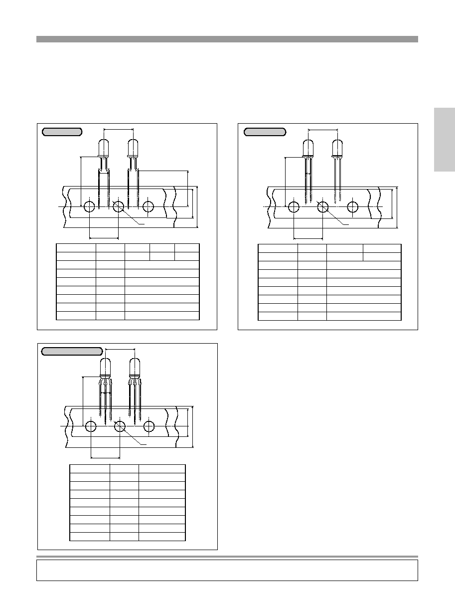
Outline Dimensions
ø3.8
ø3.0
6.0
3.5
2.5
(1.0)
10.1
±
0.5
0.4
24.0MIN
(1.0)
2.54NOM
1
2
0.4
1.7
Colored transparency
Protruded resin 0.8MAX
(Dimension from the center of ø3mm)
(Tie-bar cut)
Pin connections
1
Anode
2
Cathode
Unspecified tolerance:
±
0.2
*Outline dimensions are reference value.
GL3ZJ404B0S
GL3ZS404B0S
GL3ZV404B0S
*1 Duty ratio=1/10, Pulse width=0.1ms
*2 5s or less(At the position of 1.6mm or more from the bottom face of resin package)
Model No. Radiation color Radiation material
Power dissipation
P
(mW)
Forward current
I
F
(mA)
Derating factor
(mA/°C)
DC
Pulse
Peak forward current
I
FM
*1
(mA)
Operating temperature
T
opr
(°C)
Storage temperature
T
stg
(°C)
Soldering temperature
T
sol
*2
(°C)
Reverse voltage
V
R
(V)
(T
a
=25°C)
Orange
Sunset orange
Amber
A1GaInP on GaAs
A1GaInP on GaAs
A1GaInP on GaAs
130
130
130
50
50
50
0.67
0.67
0.67
1.33
1.33
1.33
260
260
260
100
100
100
5
5
5
-40 to +85
-40 to +85
-40 to +85
-40 to +100
-40 to +100
-40 to +100
s
Absolute Maximum Ratings
GL3ZJ404B0S
GL3ZS404B0S
GL3ZV404B0S
TYP
MAX
2.1
2.1
2.1
2.6
2.6
2.6
627
609
591
618
605
588
100
100
100
4
4
4
60
60
60
1
1
1
142
143
144
15
15
15
(570)
(530)
(540)
Model No.
Lens type
Forward voltage
V
F
(V)
p
(nm)
TYP
d
(nm)
TYP
I
V
(mcd)
TYP
(MH
Z
)
V
R
(V)
I
R
(
µ
A)
MAX
C
t
(pF)
TYP
(nm)
TYP
Peak emission
wavelength
Spectrum radiation
bandwidth
Reverse current
Page for
characteristics
diagrams
Terminal capacitance
Dominant
wavelength
Luminous
intensity
Colored
transparency
(I
F
=20mA,T
a
=25
°
C)
s
Electro-optical Characteristics
(Unit :
mm
)
4
Notice
In the absence of confirmation by device specification sheets,SHARP takes no responsibility for any defects that may occur in equipment using any SHARP devices shown in
catalogs,data books,etc.Contact SHARP in order to obtain the latest device specification sheets before using any SHARP device.
Internet
Internet address for Electronic Components Group http://www.sharp.co.jp/ecg/
s
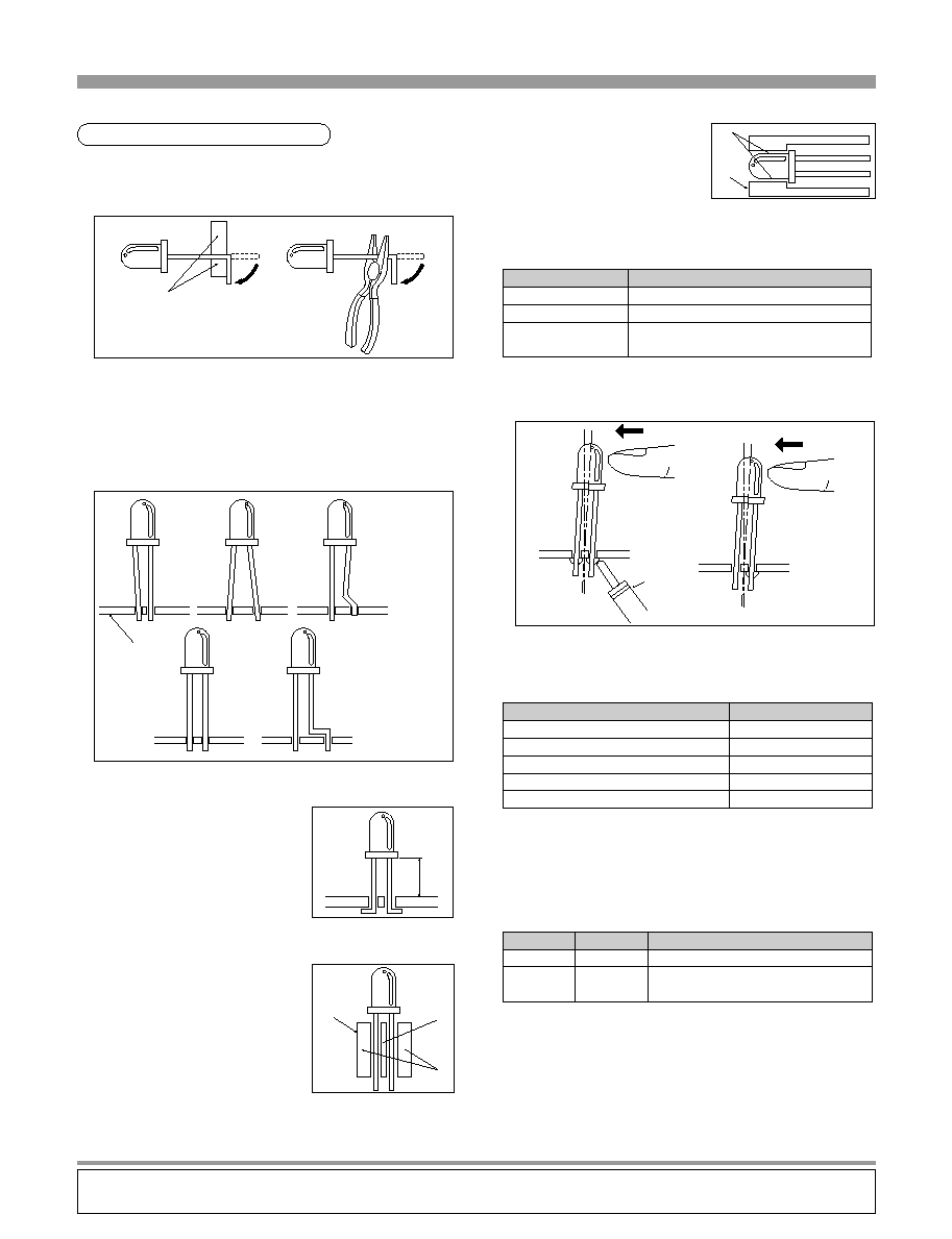
Lead Forming Method
Avoid forming a lead pin with the lead pin base as a fulcrum: be sure to hold a
lead pin firmly when forming.
Lead pins should be formed before soldering.
s
Installation
(1) Installation on a PWB
When mounting an LED lamp on a PWB, do not apply physical stress to the lead
pins.
(Notes)¡The lead pin pitch should match the PWB pin-hole pitch: absolutely avoid
widening or narrowing the lead pins.
¡When positioning an LED lamp, basically employ an LED with tie-bar cut or
use a spacer.
(2) When an LED lamp is mounted directly on a PWB
If the bottom face of an LED lamp is mounted directly on single-sided PWB, the
base of the lead pins may be subjected to have
physical stress due to PWB warp, cutting or
clinching of lead pins. Prior to use, be sure to
check that no disconnection inside of the resin
or damage to resin etc., is found.
When an LED lamp is mounted on a double-
sided PWB, the heat during soldering affects
the resin; therefore, keep the LED lamp more
than 1.6mm afloat above the PWB.
(3) Installation using a holder
During an LED lamp positioning, in case of
using a holder, holder A should be designed to
be smaller than the inside diameter of lead
pins. Holder B should be designed to be larger
than the outside diameter of lead pins.
(Notes)¡Pay attention to the thermal expansion
coefficient of the material used for the
holder. Since the holder expands and
contracts due to preheat and soldering
heat, mechanical stress may be applied to the lead pins, resulting in
disconnection.
(4) Installation to the case
Do not fix part A with adhesives when
fixed to the case as shown in the figure.
A hole of the case should be designed not
to be smaller than the outside diameter of
LED lamp resin.
s
Soldering Conditions
Solder the lead pins under the following conditions.
(Notes)¡Avoid dipping resin into soldering bath.
¡Avoid applying stress to lead pins while they are heated. For example, when the
LED lamp is moved with the heat applied to the lead pins during manual
soldering or solder repair, disconnection may occur.
s
Cleaning
(1) Solvents
The package resin may be penetrated by solvents used in cleaning. Refer to the
table below for usable solvents.
TM : Acceptable
×
: Not acceptable
(Notes)¡There is a world-wide movement to restrict the use of chrolofluorocarbon (CFC)
based solvents and we recommend that you avoid their use. However, before
using a CFC substitute solvent, carefully check that it will not penetrate the
package resin.
(2) Cleaning Methods
TM : Acceptable
: Acceptability depends on device type and conditions
(Notes)¡The affect on the device from ultrasonic cleaning differs depending on the size
of the cleaning bath, ultrasonic output, duration, board size and device mounting
method. Test the cleaning method under actual conditions and check for
abnormalities before actual use.
¡Cleaning with water is not allowed with the lead pins resin-tubulated: water may
remain, thus causing rust to the lead pins.
¡Please contact our representative before using a cleaning solvent or method not
given above.
Cleaning Method
Solvent cleaning
Ultrasonic cleaning
Usable
Remarks
Immersion up to one minute at room temperature
Test the cleaning under actual conditions and
check for abnormalities before actual use.
TM
v
Solvent
Usable
Ethyl alcohol
Isopropyl alcohol
Chlorosen
Acetone
Trichloroethylene
TM
TM
×
×
×
Soldering
iron
,,
,
,,
,
,,
,,
,
,,
,
,,
Not acceptable
Acceptable
Type of Soldering
Conditions
1. Manual soldering
2. Wave soldering
3. Reflow soldering
295°C
±
5°C, within 3 seconds
260°C
±
5°C, within 5 seconds
Preheating 70°C to 80°C, within 30 seconds
Soldering 245°C
±
5°C, within 5 seconds
,
,,
,
,
,,
,
,
,,
,
,
,,
,
,
,,
,
PWB
Not acceptable
Acceptable
,
,,,
,
Hold a lead pin firmly when forming
A: Lead Pin Type
,,
,,
,,
,,
,,
,
,
1.6
A
,
,,
,,,
,
,,
,,,
,,
,
Case
A
,,
,,
,,
,,
,,
,,
,
Holder
A
B
General Description of Light Emitting Diodes
v
142
Notice
In the absence of confirmation by device specification sheets,SHARP takes no responsibility for any defects that may occur in equipment using any SHARP devices shown in
catalogs,data books,etc.Contact SHARP in order to obtain the latest device specification sheets before using any SHARP device.
Internet
Internet address for Electronic Components Group http://www.sharp.co.jp/ecg/
LED Lamp
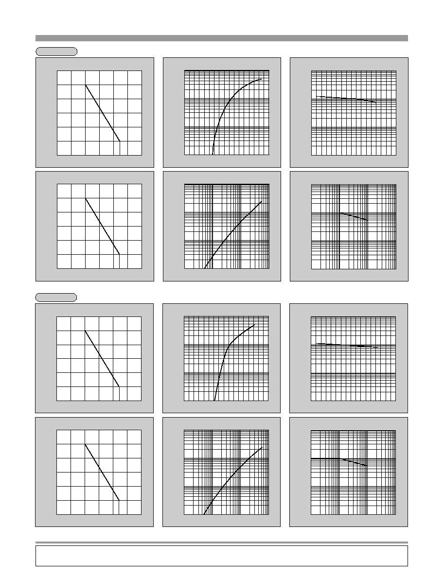
Characteristics Diagrams
ZJ series
0
10
20
30
40
50
60
-40
0
25
50
75
125
00
85
Forward Current Derating Curve
Ambient temperature T
a
(°C)
Forward current I
F
(mA)
5.0
1.0
0.1
0.5
10
50
100
1.0
1.2
1.4
1.6
1.8
2.0
2.2
2.4
2.6
Forward Current vs. Forward Voltage(Note)
Forward voltage V
F
(V)
Forward current I
F
(mA)
(T
a=
25°C)
(1
F
=20mA)
1.0
10
5.0
50
100
500
1000
-20
-40
0
20
40
60
100
80
Luminous Intensity vs. Ambient Temperature(Note)
Ambient temperature T
a
(°C)
Relative luminous intensity(%)
0
20
40
60
80
100
120
-40
0
25
50
75 85
125
100
Peak Forward Current Derating Curve
Ambient temperature T
a
(°C)
Peak forward current I
FM
(mA)
Luminous Intensity vs. Forward Current(Note)
Forward current I
F
(mA)
Relative luminous intensity(%)
(T
a=
25°C)
1.0
2.0
5.0
200
500
100
20
50
10
1000
0.1
0.2
0.5
1
2
5
10
20
50
1/50
1/20 1/10
1/5
1/2
1
Duty Ratio vs. Peak Forward Current
Duty ratio D
R
Peak forward current I
F
(mA)
(T
a=
25°C)
1
2.0
5.0
200
100
30
50
10
500
Note)Characteristics shown in diagrams are typical values. (not assurance value)
ZR series
0
10
20
30
40
50
60
-40
0
25
50
75 85
125
100
0.1
0.5
1.0
5.0
10
50
100
1.0
1.2
1.4
1.6
1.8
2.0
2.4
2.6
2.2
Forward Current vs. Forward Voltage(Note)
Forward voltage V
F
(V)
Forward current I
F
(mA)
(T
a=
25°C)
1.0
5.0
10
50
100
500
1000
-40
-20
0
20
40
60
100
80
Luminous Intensity vs. Ambient Temperature(Note)
Ambient temperature T
a(
°C)
Relative luminous intensity(%)
(1
F
=20mA)
0
20
40
60
80
100
120
-40
0
25
50
75 85
125
100
Peak Forward Current Derating Curve
Ambient temperature T
a
(°C)
Peak forward current I
FM
(mA)
1.0
5.0
2.0
10
20
50
100
200
500
1000
0.1
0.2
0.5
1
2
5
10
20
50
Luminous Intensity vs. Forward Current(Note)
Forward current I
F
(mA)
Relative luminous intensity(%)
(T
a=
25°C)
1.0
5.0
2.0
10
20
50
100
200
500
1/50
1/20 1/10
1/5
1/2
1
Duty Ratio vs. Peak Forward Current
Duty ratio D
R
Peak forward current I
FM
(mA)
(T
a=
25°C)
Forward Current Derating Curve
Ambient temperature T
a
(°C)
Forward current I
F
(mA)
143
Notice
In the absence of confirmation by device specification sheets,SHARP takes no responsibility for any defects that may occur in equipment using any SHARP devices shown in
catalogs,data books,etc.Contact SHARP in order to obtain the latest device specification sheets before using any SHARP device.
Internet
Internet address for Electronic Components Group http://www.sharp.co.jp/ecg/
LED
Lamp
LED Lamp
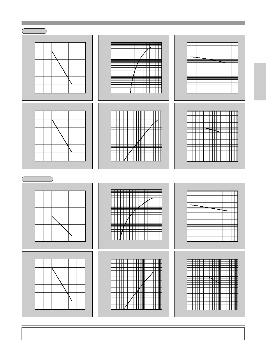
Characteristics Diagrams
Note)Characteristics shown in diagrams are typical values. (not assurance value)
0
10
20
30
40
50
60
-40
0
25
50
75 85
125
100
Forward Current Derating Curve
Ambient temperature T
a
(°C)
Forward current I
F
(mA)
0
20
40
60
80
100
120
-40
0
25
50
75 85
125
100
Peak Forward Current Derating Curve
Ambient temperature T
a
(°C)
Peak forward current I
FM
(mA)
0.1
0.5
1.0
5.0
10
50
100
1.4
1.6
1.8
2.0
2.2
2.4
2.8
3.0
2.6
Forward Current vs. Forward Voltage(Note)
Forward voltage V
F
(V)
Forward current I
F
(mA)
1.0
5.0
10
50
100
500
1000
-40
-20
0
20
40
60
80
100
Luminous Intensity vs. Ambient Temperature(Note)
Ambient temperature T
a(
°C)
Relative luminous intensity(%)
(I
F
=
20mA)
1.0
5.0
2.0
10
20
50
100
200
500
1000
0.1
0.2
0.5
1
2
5
10
20
50 100
Luminous Intensity vs. Forward Current(Note)
Forward current I
F
(mA)
Relative luminous intensity(%)
1.0
5.0
2.0
10
20
50
100
200
500
1000
1/50
1/20 1/10
1/5
1/2
1
10
Duty Ratio vs. Peak Forward Current
Duty ratio D
R
Peak forward current I
FM
(mA)
GL5XS022BOS
ZS series
0
20
40
60
80
100
120
-40
0
25
50
75 85
125
100
Peak Forward Current Derating Curve
Ambient temperature T
a
(°C)
Peak forward current I
FM
(mA)
0
10
20
30
40
50
60
-25
0
25
50
75 85
125
100
Forward Current Derating Curve
Ambient temperature T
a
(°C)
Forward current I
F
(mA)
0.1
0.5
1.0
5.0
10
50
100
1.0
1.2
1.4
1.6
1.8
2.0
2.4
2.6
2.2
Forward Current vs. Forward Voltage(Note)
Forward voltage V
F
(V)
Forward current I
F
(mA)
1.0
5.0
10
50
100
500
1000
-40
-20
0
20
40
60
100
80
Luminous Intensity vs. Ambient Temperature(Note)
Ambient temperature T
a(
°C)
Relative luminous intensity(%)
(1
F
=20mA)
1.0
5.0
2.0
10
20
50
100
200
500
1000
0.1
0.2
0.5
1
2
5
10
20
50
Luminous Intensity vs. Forward Current(Note)
Forward current I
F
(mA)
Relative luminous intensity(%)
1.0
5.0
2.0
10
20
50
100
200
500
1/50
1/20 1/10
1/5
1/2
1
Duty Ratio vs. Peak Forward Current
Duty ratio D
R
Peak forward current I
FM
(mA)
(T
a=
25
°C
)
(T
a=
25
°C
)
(T
a=
25
°C
)
(T
a=
25
°C
)
(T
a=
25
°C
)
(T
a=
25
°C
)