 | –≠–ª–µ–∫—Ç—Ä–æ–Ω–Ω—ã–π –∫–æ–º–ø–æ–Ω–µ–Ω—Ç: GP1A30R | –°–∫–∞—á–∞—Ç—å:  PDF PDF  ZIP ZIP |
GP1A30R
GP1A30R
*3 Measured under the condition shown in Measurement Conditions.
*4 In the condition that output A and B are low level.
t
AH
t
AP
t
BP
t
BH
s
Electro-optical Characteristics
( Unless otherwise specified, Ta = 0 to + 70∞C)
*2 For 5 seconds
Parameter
Symbol
Conditions
MIN.
TYP.
MAX.
Unit
Input
Forward voltage
V
F
Ta= 25∞C, I
F
= 30mA
-
1.2
1.5
V
Reverse current
I
R
Ta= 25∞C, V
R
= 3V
-
-
10
µ
A
Output
Operating supply voltage
V
CC
4.5
5.0
5.5
V
High level output voltage
V
OH
V
CC
= 5V, I
F
= 30mA
*3
2.4
4.9
-
V
Low level output voltage
V
OL
I
OL
= 8mA, V
CC
= 5V, I
F
= 30mA
*3
-
0.1
0.4
V
Supply current
I
CC
-
5
20
mA
Transfer
charac-
teristics
Duty ratio
V
CC
= 5V, I
F
= 30mA,
f= 2.5kHz
*3
Response frequency
f
MAX.
V
CC
= 5V, I
F
= 30mA
*3
-
-
5
kHz
s
Absolute Maximum Ratings
(Ta= 25∞C )
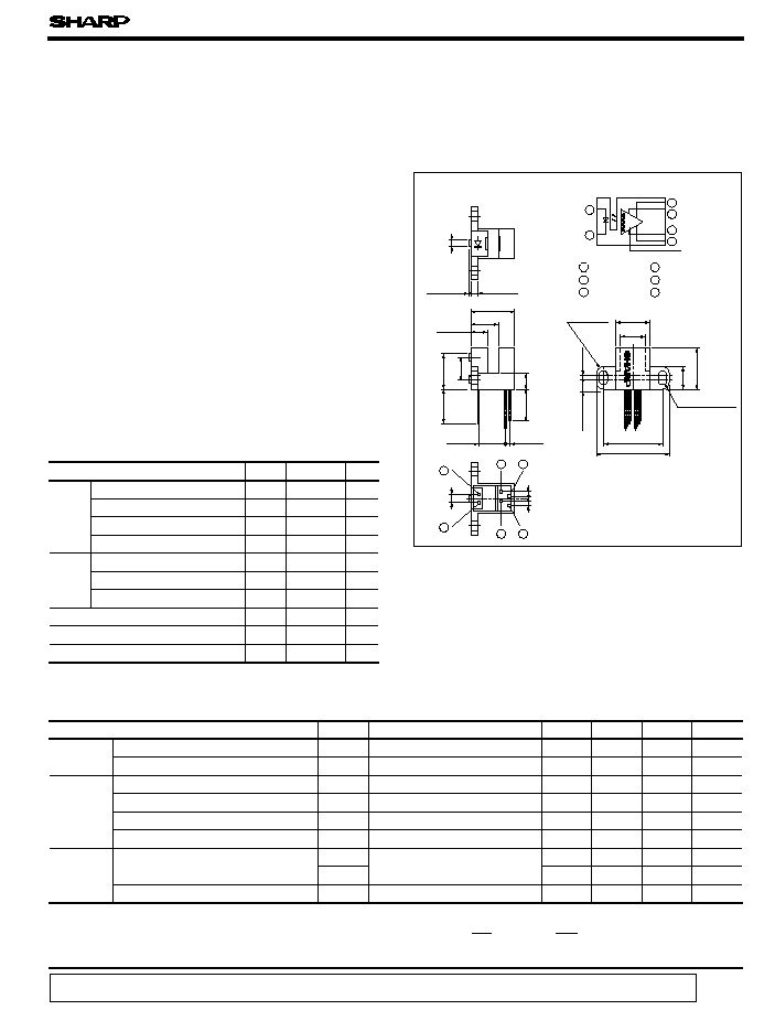
OPIC Photointerrupter with Encoder
Function
s
Features
1. 2-phase ( A, B ) digital output
2. Possible to use plastic disk
3. High sensing accuracy
( Disk slit pitch : 0.7mm )
4. TTL compatible output
5. Compact and light
s
Applications
1. Electronic typewriters, printers
2. Numerical control machines
s
Outline Dimensions
(Unit : mm )
*5
D
A
B
=
I
F
= 30mA, V
CC
= 5V
Parameter
Symbol
Rating
Unit
Input
Forward current
I
F
65
mA
*1
Peak forward current
I
FM
1
A
Reverse voltage
V
R
6
V
Power dissipation
P
100
mW
Output
Supply voltage
V
CC
7
V
Low level output current
I
OL
20
mA
Power dissipation
P
O
250
mW
Operating temperature
T
opr
0 to + 70
∞C
Storage temperature
T
stg
- 40 to + 80
∞C
*2
Soldering temperature
T
sol
260
∞C
OPIC
12.0
9.9
4.4
(7.25)
(1.27)
6.0
8.0
( 2.54
)
4
-
R2.5
20.0
3
-
( 1.27
)
GP1A30R
Internal connection diagram
OPIC
1
2
3
4
5
6
1 Anode
2 Cathode
4 GND
1
2
3
4
5
6
D
A
*5
D
B
*5
6.4
11.4
3 V
OB
4
±
0.15
*1 Pulse width <= 100
µ
s, Duty ratio= 0.01
20
20
50
50
80
80
%
%
x 100
An OPIC consists of a light-detecting element and signal-
processing circuit integrated onto a single chip.
*" OPIC" (Optical IC ) is a trademark of the SHARP Corporation.
data books, etc. Contact SHARP in order to obtain the latest version of the device specification sheets before using any SHARP's device.
"
"
In the absence of confirmation by device specification sheets, SHARP takes no responsibility for any defects that occur in equipment using any of SHARP's devices, shown in catalogs,
*
Tolerance
:±
0.3mm
*
( )
:
Reference dimensions
*3*4
=
x 100, D
5 V
CC
6 V
OA
2
-
2.0
±
0.1
0.8
±
0.15
2.0
±
0.15
7.5
±
0.1
6.4
±
0.15
2.5
±
0.15
1.4
±
0.15
4
-
R1.3
±
0.15
15.0
±
0.15
8.0
MIN.
10.5
MIN.
GP1A30R
s
Output Waveforms
t
AH
t
AP
t
AB1
t
BH
t
BP
Output A
( V
OA
)
Output B
( V
OB
)
Rotational direction
:
Counterclockwise when seen
70
0
25
50
75
100
60
50
40
30
20
10
0
70
0
50
100
150
200
250
300
100
75
50
25
0
(Output B )
1
10
2
5
Frequency f ( kHz )
0.6
0.7
0.1
0.2
0.3
0.4
0.5
90
80
70
100
110
120
130
70
80
90
100
65
20
0.9
0.8
1
2
5
10
20
50
60
V
CC
= 5V
I
F
= 30mA
AB1
=x
360∞
t
ABI
t
AP
Phase difference
AB1
Ambient Temperature
Temperature
( Output A )
Ambient temperature T
a
(∞C)
Output power dissipation P
o
(
mW
)
Ambient temperature T
a
(∞C)
Forward current I
F
(
mA
)
Fig. 1 Forward Current vs. Ambient
Fig. 2 Output Power Dissipation vs.
Fig. 3 Duty Ratio vs. Frequency
Fig. 4 Phase Difference vs. Frequency
Duty ratio
(
deg.
)
Frequency f ( kHz )
V
CC
= 5V
I
F
= 30mA
t
AH
t
AP
t
BH
t
BP
T
a
= 25∞C
T
a
= 25∞C
from OPIC light detector
GP1A30R
( Output A )
( Output B )
f = 2.5kHz
Duty ratio
0.4
0.3
0.2
0.1
0
0.6
0.5
25
0
50
75
100
130
120
110
100
90
80
70
Distance X ( mm ) ( Shifting encoder )
( Output B )
( Output A )
0.6
0.7
0.1
0.2
0.3
0.4
0.5
Duty ratio
f= 2.5kHz
1.0
0
- 1.0
Duty ratio
Distance Y ( mm ) ( Shifting encoder )
( + )
( - )
GP1A30R
Disk
Reference position
Distance X ( mm ) ( Shifting encoder )
70
80
90
100
110
120
130
position
Distance Y ( mm ) ( Shifting encoder )
( - )
( + )
1.0
0.9
0.8
0.7
f = 2.5kHz
100
75
50
0
25
40
50
60
140
- 0.5
0.5
0.9
0.8
- 1.0
- 0.5
0
0.5
1.0
0.8
0.9
0.5
0.4
0.3
0.2
0.1
0.7
0.6
f= 2.5kHz
- 1.0
- 0.5
0
0.5
1.0
f= 2.5kHz
- 1.0
- 0.5
0
0.5
1.0
50
60
60
50
130
120
110
100
90
80
70
f= 2.5kHz
( Output A)
( Output B)
Disk
GP1A30R
V
CC
= 5V
I
F
= 30mA
t
AH
t
BH
t
AP
t
BP
V
CC
= 5V
I
F
= 30mA
AB1
=
x 360∞
t
AB1
t
AP
V
CC
= 5V
I
F
= 30mA
V
CC
= 5V
I
F
= 30mA
V
CC
= 5V
I
F
= 30mA
AB1
=
x 360∞
t
AB1
t
AP
V
CC
= 5V
I
F
= 30mA
t
AH
t
AP
t
BH
t
BP
Temperature
Ambient temperature T
a
(∞C)
Ambient temperature T
a
(∞C)
Phase difference
AB1
Phase difference
AB1
Phase difference
AB1
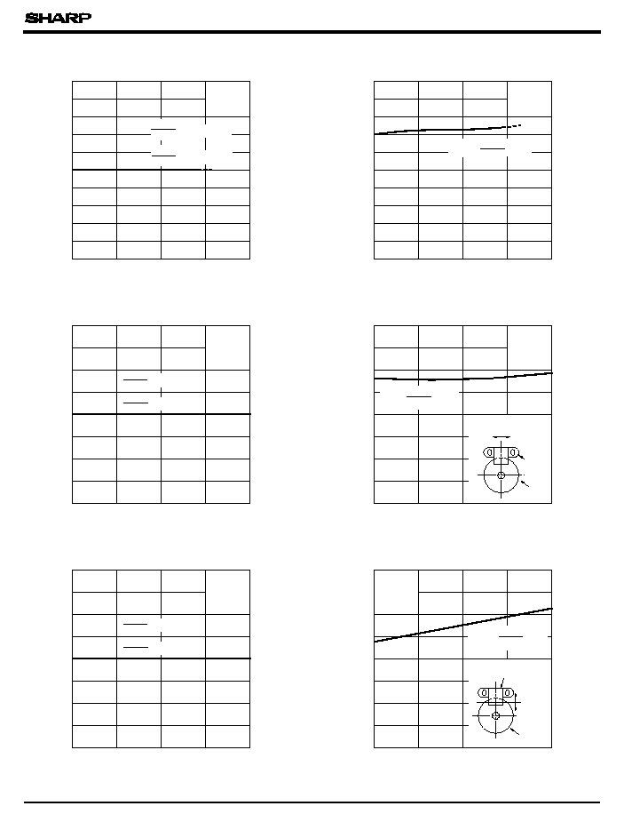
Fig. 5 Duty Ratio vs. Ambient Temperature
Fig. 6 Phase Difference vs. Ambient
Fig. 8 Phase Difference vs.
T
a
= 25∞C
Fig.10 Phase Difference vs.
(
deg.
)
(
deg.
)
(
deg.
)
t
ABI
t
AP
AB1
=
x 360∞
Reference
t
AH
t
AP
t
BH
t
BP
T
a
= 25∞C
T
a
= 25∞C
T
a
= 25∞C
Fig. 7 Duty Ratio vs. Distance (X direction )
Distance (X direction )
Distance ( Y direction )
Fig. 9 Duty Ratio vs. Distance (Y direction )

GP1A30R
0.9
0.8
0.7
0.6
0.5
0.4
0.3
0.2
0.1
0
f= 2.5kHz
Duty ratio
( Output A )
( Output B )
Distance Z ( mm ) ( Shifting encoder )
0.1
0.2
0.3
0.4
0.5
0.6
0.7
0.8
50
70
80
90
100
110
120
130
60
f= 2.5kHz
Distance Z ( mm ) ( Shifting encoder )
Disk
( Detecting side )
( Emitting side )
OPIC
Z
0
0.1
0.2
0.3
0.4
0.5
0.6
0.7
0.8
15
20
1.4
6.4
(18.385 )
A
4-R1.3
Disk center
Disk
8
9.9
7.5
12
11.4
0.3
2
0.8 A
P
Disk center
Enlarged drawing
of A portion
Slit pitch
:
P
(11.685 )
V
CC
= 5V
I
F
= 30mA
V
CC
= 5V
I
F
= 30mA
t
AH
t
AP
t
BH
t
BP
AB1
=
x 360∞
t
AB1
t
AP
GP1A30R
r
1
=
r
2
r
1
r
2
S
2
S
1
Phase difference
AB1
T
a
= 25∞C
Fig.12 Phase Difference vs.
<Basic Design>
R
O
=
x 1 3 . 4 5 ( mm )
N: number of slits
S
1
= R
O
- 1.765 (mm ), S
2
= S
1
+ 6.7(mm )
R
O
( distance between the disk center and half point of a slit ) ,
P ( slit pitch ) , S
1
Slit pitch : P ( slit center )
120
are also changed according to the number.
120
R
O
=
x 13.45 ( mm )
= 22.42mm
= 0.704mm
S
1
= 22.42- 1.765
= 20.655mm
S
2
= 20.655+ 6.7
= 27.355mm
N= 200P/R
s
Measurement Conditions
s
Precautions for Use
31.6, 0.1t
120 slits
( 1) This module is designed to be operated
at I
F
= 30mA TYP.
( 2) Fixing torque : MAX. 0.6Nm 6kgf ∑ cm
(
)
( 3) In order to stabilize power supply line,
connect a by-pass capacitor of more than 0.01
µ
F
between Vcc and GND near the device.
(
deg.
)
and S
2
( installing position of photointer-
200
2 x p x 22.42
P=
( mm )
200
( Ex. ) In the case of
rupter ) will be provided by the following equations.
Note ) When the number of slits is changed, values in parenthesis
N
N
2x p x R
O
P=
( mm )
( 4) As for other general cautions, refer to
T
a
= 25∞C
the chapter " Precautions for Use " .
Fig.11 Duty Ratio vs. Distance (Z direction )
Distance (Z direction )
R13.45
3
4