 | –≠–ª–µ–∫—Ç—Ä–æ–Ω–Ω—ã–π –∫–æ–º–ø–æ–Ω–µ–Ω—Ç: GP1A68L | –°–∫–∞—á–∞—Ç—å:  PDF PDF  ZIP ZIP |
(Ta=25∞C)
I
F
50
mA
V
R
6
V
P
75
mW
V
CC
7
V
I
mA
P
O
80
mW
T
opr
∞C
T
stg
∞C
T
sol
260
∞C
0.15
2.54
0.4
1.27 1.27
3
4
5
2
1
5
4
3
1
2
5 GND
(1.0
)
(15k
)
g
3.8
±
0.2
0.9
±
0.2
1.45
±
0.2
4.0
±
0.2
5.0
±
0.2
4.0
±
0.2
4
MIN.
2.5
±
0.2
3 V
CC
4 V
out
Features
Applications
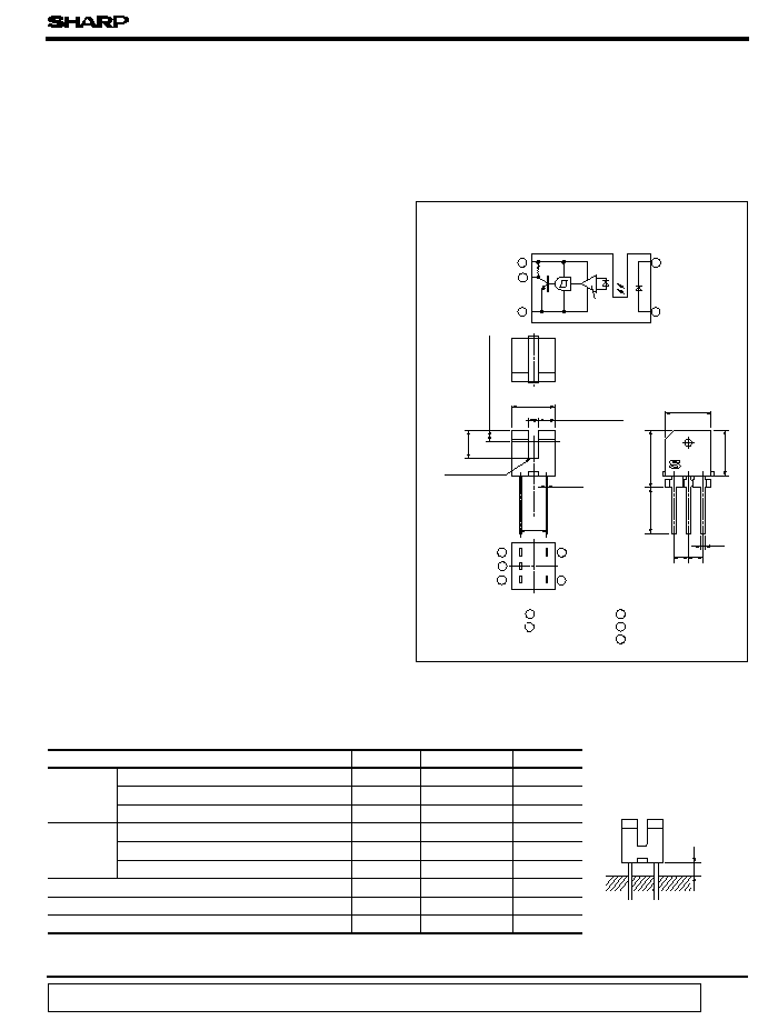
Outline Dimensions
(Unit : mm)
Internal connection diagram
Amp.
Optical center
1 Anode
2 Cathode
* "OPIC" (Optical IC) is a trademark of the SHARP Corporation.
An OPIC consists of a light-detecting element and
signal-processing circuit integrated onto a single chip.
Absolute Maximum Ratings
Parameter
Symbol
Rating
Unit
*1
Forward current
Reverse voltage
Power dissipation
Supply voltage
Low level output current
Power dissipation
Operating temperature
Storage temperature
Soldering temperature
Input
Output
- 25 to + 85
- 40 to + 100
MIN. 1mm
Soldering area
*1 For 5 seconds
GP1A68L
GP1A68L
2
(2
-
C0.3)
1. Ultra-compact type (3.8 x 4.0 x 4.0 mm)
2. C-MOS and microcomputer compatible
3. Low voltage driven, low current consumption
(Operating supply voltage : 1.4 to 7.0V,
Standby current consumption : MAX. 0.5mA)
1. Cameras
2. Floppy disk drives
(Sensor center)
Low Voltage Driven Low Current
Consumption Type OPIC
Photointerrupter
OL
data books, etc. Contact SHARP in order to obtain the latest version of the device specification sheets before using any SHARP's device.
"
"
In the absence of confirmation by device specification sheets, SHARP takes no responsibility for any defects that occur in equipment using any of SHARP's devices, shown in catalogs,
s
s
s
s

(Ta=25 ∞C)
15k
GND
47
t
r
=
t
f
Z
O
=
50
1.5V
50
%
t
t
V
OH
90
%
10
%
V
OL
t
r
t
f
V
F
I
F
-
V
I
R
V
R
= 3V
-
-
10
µ
A
V
CC
-
7.0
V
V
OL
V
CC
OL
F
= 5mA
-
0.4
V
V
OH
-
-
V
I
CCL
V
CC
F
= 5mA
-
mA
I
CCH
V
CC
F
= 0
-
mA
I
FHL
V
CC
-
0.9
2.5
mA
I
FLH
/I
V
CC
0.55
0.8
0.95
-
"Low
High"
propagation delay time
t
PLH
V
CC
I
F
= 5mA
R
L
-
30
"High
Low"
propagation delay time
t
PHL
-
3.0
15
t
r
-
t
-
V
CC
F
= 0
0
10
20
30
40
50
60
100
75
50
25
0
- 25
- 25
0
25
50
75
100
100
80
60
40
20
0
FHL
f
µ
s
=
0.01
µ
s
PHL
PLH
0.1
µ
F
Electro-optical Characteristics
Parameter
Symbol
Conditions
MIN.
TYP.
MAX.
Unit
Input
Output
Transfer
characteristics
Forward voltage
Reverse current
Operating supply voltage
Rise time
Fall time
Low level
output voltage
High level
output voltage
Low level
supply current
High level
supply current
Hysteresis
*2
*2 I represents forward current when output goes from "High" to "Low".
FHL
Test Circuit for Response Time
Input
Output
Amp.
Input
Output
Output
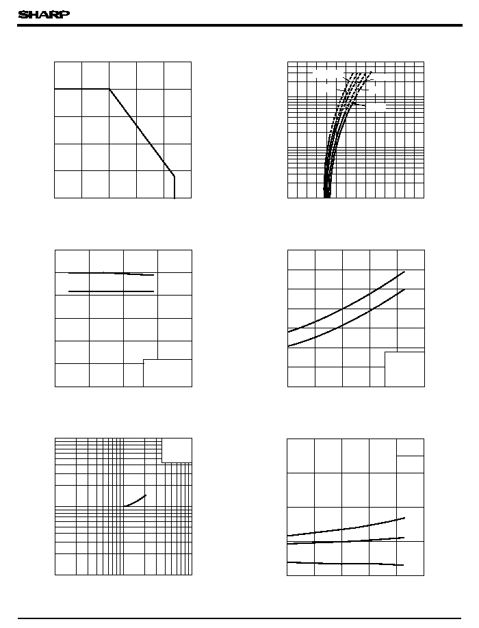
Fig. 1 Forward Current vs. Ambient
Temperature
Fig. 2 Power Dissipation vs. Ambient
Temperature
Forward current I
F
(
mA
)
Ambient temperature Ta (∞C)
Ambient temperature Ta (∞C)
Power dissipation P (mW)
GP1A68L
= 5mA
1.15
1.25
1.4
0.1
2.9
0.7
0.3
1.2
0.5
10
0.6
0.2
3
1.0
= 3V
= 3V
= 3V
"High
Low"
threshold input current
*3
= 3k
+
3V
3k
-
= 3V,I
= 3V,I
= 3V,I
= 3V,I
Response time
= 1mA,I
*3 Hysteresis stands for I /I .
FLH FHL
Output side power dissipation
Input side power dissipation
s
- 25
85
0
25
50
75
100
0
3.5
0
0.5
1
1.5
2
2.5
3
500
200
100
50
20
10
5
2
1
50∞C
25∞C
0∞C
- 25∞C
T
a
= 75∞C
Fig. 3 Low Level Output Current vs.
Ambient Temperature
Fig. 4 Forward Current vs. Forward Voltage
Fig. 8 Low Level Output Voltage vs.
Ambient Temperature
Low level output current I
OL
(
mA
)
Forward current I
F
(
mA
)
Ambient temperature Ta (∞C)
Forward voltage V
F
(V)
Supply voltage V
CC
(V)
Relative threshold input current I
FHL
, I
FLH
Relative threshold input current
Ambient temperature Ta (∞C)
Ambient temperature Ta (∞C)
Low level output voltage V
OL
(
V
)
Low level output current I
OL
(mA)
Low level output voltage V
OL
(
V
)
GP1A68L
2.5
2.0
1.5
1.0
0.5
Fig. 5 Relative Threshold Input Current
vs. Supply Voltage
Fig. 6 Relative Threshold Input Current
vs. Ambient Temperature
Fig. 7 Low Level Output Voltage vs.
Low Level Output Current
- 25
0
25
50
75
100
0.0
V
CC
=3V
I
F
=5mA
I
OL
=2mA
I
OL
=1mA
I
OL
=0mA
0.1
0.2
0.3
0.4
0.1
0.2
0.5
1
2
5
10
0.01
Ta=25∞C
V
CC
=3V
I
F
=5mA
0.10
1.00
- 25
0
25
50
75
100
0.2
1.2
1.4
1.6
I
FHL
I
FLH
V
CC
=3V
∞C
1.0
0.8
0.6
0.4
0
2.5
5.0
7.5
10.0
0
1.0
1.2
I
FHL
I
FLH
Ta=25∞C
I
at Vcc=3V
0.8
0.6
0.4
0.2
FHL
=1
I
at Ta=25
FHL
=1
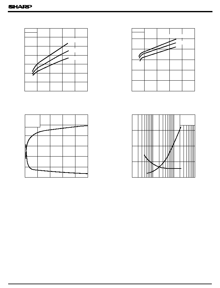
Fig. 10 High Level Supply Current vs.
Supply Voltage
Fig. 9 Low Level Supply Current vs.
Supply Voltage
Fig. 11 Propagation Delay Time vs.
Forward Current
Low level supply current I
CCL
(
mA
)
Supply voltage V
CC
(V)
Supply voltage V
CC
(V)
Forward current I
F
(mA)
Load resistance R
L
(k
)
GP1A68L
(Precautions for Operation)
1) It is recommended that a by-pass capacitor of 0.1
µ
F or more between Vcc and GND near
the device in order to stabilize power supply line.
2) As for other general precautions, refer to the the chapter "Precautions for Use".
Fig. 12 Rise, Fall Time vs. Load Resistance
High level supply current I
CCH
(
mA
)
Propagation delay time t
PHL
,t
PLH
(
µ
s)
Rise, fall time t
r
,t
f
(
µ
s)
0.1
1
10
100
0
0.3
0.2
0.1
0.4
V
CC
= 5V
I
F
= 5mA
Ta= 25∞C
t
r
t
r
0
10
20
30
40
50
0
10
8
6
4
2
12
V
CC
= 3V
R
L
= 3k
Ta= 25∞C
t
PHL
t
PLH
0
2
4
6
8
10
0.0
0.5
0.4
0.3
0.2
0.1
0.6
I
F
= 0mA
Ta= 85∞C
Ta=- 25∞C
Ta= 25∞C
0
2
4
6
8
10
0.0
1.0
1.2
1.4
I
F
= 5mA
0.8
0.6
0.4
0.2
Ta=- 25∞C
Ta= 25∞C
Ta= 85∞C