 | –≠–ª–µ–∫—Ç—Ä–æ–Ω–Ω—ã–π –∫–æ–º–ø–æ–Ω–µ–Ω—Ç: GP1S21 | –°–∫–∞—á–∞—Ç—å:  PDF PDF  ZIP ZIP |

s
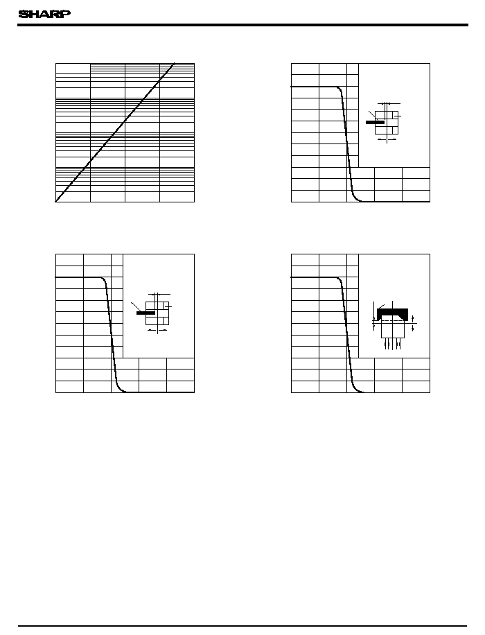
Outline Dimensions
(Unit : mm )
GP1S21/GP1S22
GP1S21/GP1S22
s
Absolute Maximum Ratings
(Ta = 25∞C )
Subminiature Photointerrupter
s
Features
s
Applications
1. Ultra-compact
2. PWB mounting type package
*1 For 5 seconds
2. Floppy disk drives
1. Cameras
Parameter
Symbol
Rating
Unit
Input
Forward current
I
F
50
mA
Reverse voltage
V
R
6
V
Power dissipation
P
75
mW
Output
Collector-emitter voltage
V
CEO
35
V
Emitter-collector voltage
V
ECO
6
V
Collector current
I
C
20
mA
Collector power dissipation
P
C
75
mW
Total power dissipation
P
tot
100
mW
Operating temperature
T
opr
- 25 to + 85
∞C
Storage temperature
T
stg
- 40 to + 100
∞C
*1
Soldering temperature
T
sol
260
∞C
diagram
Internal connection
4.2
1.5 1.2
g
3.1
(C0.3)
4
-
0.15
( 1.0
)
2.8
5.2
4.2
3.9
g
2.5
Rest of gate
(2)
(C0.8)
1
3
1
1 Anode
3
5
Slit width
5
Slit width
1mm or more
3. High sensing accuracy
GP1S22
: 0.3mm
(
)
Slit width ;
GP1S21
: 0.8mm
from the lead base.
GP1S21
:
0.8mm
GP1S22
:
0.3mm
4
-
0.5
3 Emitter
Soldering area
2
4
2 Cathode
4 Collector
*
Tolerance
:±
0.2mm
*
Burr's dimensions
:
0.15MAX.
*
Rest of gate
:
0.3MAX.
*
( )
:
Reference dimensions
*
The dimensions indicated by
g
refer to those measured
4
2
(Light axis)
data books, etc. Contact SHARP in order to obtain the latest version of the device specification sheets before using any SHARP's device.
"
"
In the absence of confirmation by device specification sheets, SHARP takes no responsibility for any defects that occur in equipment using any of SHARP's devices, shown in catalogs,
4.0
MIN.
1.5
+
0.1
-
0
Hole

(Ta = 25∞C )
s
Electro-optical Characteristics
GP1S21/GP1S22
Parameter
Symbol
Conditions
MIN.
TYP.
MAX.
Unit
Input
Forward voltage
V
F
I
F
= 20mA
-
1.2
1.4
V
Reverse current
I
R
V
R
= 3V
-
-
10
µ
A
Output
Collector dark current
I
CEO
V
CE
= 20V
-
-7
A
Transfer
charac-
teristics
-
µ
A
-
µ
A
Collector-emitter
saturation voltage
V
CE( sat )
-
-
0.4
V
-
-
0.4
V
Response time
-
µ
s
-
µ
s
GP1S21
GP1S22
GP1S21
GP1S22
Rise time
Fall time
t
r
t
f
V
CE
= 5V, I
F
= 1.5mA
V
CE
= 5V, I
F
= 5mA
I
F
= 3mA, I
C
= 27
µ
A
I
F
= 10mA, I
C
= 50
µ
A
27
100
-
50
50
150
150
260
1300
I
C
= 0.1mA, V
CE
= 5V, R
L
= 1k
- 25
0
25
50
75
100
0
10
20
30
40
50
60
- 25
0
25
50
75
100
0
20
40
60
Power dissipation P
(
mW
)
80
0
0.5
1
1.5
2
1
2
10
20
100
200
2.5
3
5
50
500
25∞C
0∞C
- 25∞C
50∞C
3.5
85
100
120
0
2
0
0.2
1.6
1
1.0
1.4
1.2
0.4
0.6
0.8
10
3
4
5
6
7
8
9
1.8
2.0
85
Forward current I
F
(
mA
)
Ambient temperature T
a
(∞C)
Ambient temperature T
a
(∞C)
P
tot
P, P
c
T
a
= 75∞C
Forward current I
F
(
mA
)
Forward voltage V
F
(V)
Collector current I
C
(
mA
)
Forward current I
F
( mA )
GP1S21
GP1S22
Fig. 2 Power Dissipation vs.
Ambient Temperature
Fig. 3 Forward Current vs.
Forward Voltage
Fig. 4 Collector Current vs.
Forward Current
Fig. 1 Forward Current vs. Ambient
Temperature
V
CE
= 5V
T
a
= 25∞C
1 x 10
Collector Current
Ic

2
3
4
5
6
7
8
9
10
1
0
2
3
4
5
6
7
8
9
10
1
0
11
0
1
10
9
8
7
6
5
4
3
2
11
10
9
8
7
6
5
4
3
2
1
0
25
50
75
100
0
-25
-25
0
100
75
50
25
0.1
0.2
0.3
0.4
0.5
0.6
0
0.02
0.04
0.06
0.08
0.10
0.12
0.14
0.16
0
0.1
0.5
0.01
0.2
1
2
5
10
20
50 100
1
0.5
0.3
2
5
10
20
50
100
200
500
10
%
Test Circuit for Response Time
Output
Input
90
%
Input
Output
40mA
30mA
20mA
10mA
5mA
P
C
( MAX. )
I
F
= 50mA
Collector current I
C
(
mA
)
Collector-emitter voltage V
CE
(V)
P
C
( MAX. )
I
F
= 50mA
Collector current I
C
(
mA
)
Collector-emitter voltage V
CE
(V)
GP1S22
GP1S21
Collector current I
C
(
mA
)
Ambient temperature T
a
(∞C)
V
CE
( sat
)
(V
)
Ambient temperature T
a
(∞C)
GP1S21
GP1S22
t
f
t
r
t
d
t
s
R
D
V
CC
R
L
t
d
t
s
t
r
t
f
Ambient Temperature
GP1S21/GP1S22
40mA
30mA
20mA
10mA
1.5mA
(GP1S21)
V
CE
= 5V
I
F
= 1.5mA (
GP1S21
)
I
F
= 3mA (
I
F
= 10mA (
I = 27
µ
A (
I = 50
µ
A (
V
CE
I
C
= 100
µ
A
T
a
= 25∞C
Fig. 5-a Collector Current vs. Collector-emitter
Fig. 5-b Collector Current vs. Collector-emitter
Fig. 6 Collector Current vs.
Fig. 7 Collector-emitter Saturation
Voltage vs. Ambient Temperature
C
C
Collector-emitter saturation voltage
Response time
(
µ
s
)
= 5V
Voltage
Voltage
(GP1S22 )
GP1S22
)
GP1S21
)
GP1S22
)
GP1S21
)
I
F
= 5mA (
GP1S22
)
Fig. 8 Response Time vs. Load Resistance
Load resistance R
L
( k
)
2
5
2
5
2
5
2
5
25
50
75
100
0
3
2
1
0
0
50
100
0
+
L
Detector
( Detector center)
Shield
Shield distance L ( mm )
Relative collector current
(
%
)
Shield
( Detector center )
Detector
L
+
0
100
50
0
-2
-1
0
1
2
3
Shield distance L ( mm )
Relative collector current
(
%
)
Shield
(
Detector center
)
Detector
0
100
50
0
-2
-1
0
1
2
3
L
+
I
F
= 1.5mA
V
CE
= 5V
T
a
= 25∞C
V
CE
= 20V
Shield Distance (2)
I
F
V
CE
= 5V
T
a
= 25∞C
Ambient Temperature
GP1S21/GP1S22
(GP1S21)
Shield Distance (1)
(GP1S22)
I
F
= 1.5mA (
GP1S21
)
GP1S22
)
Fig. 9 Collector Dark Current vs.
Fig.11 Relative Collector Current vs.
-
-
Fig. 10-a Relative Collector Current vs.
Shield Distance ( 1 )
Relative collector current
(
%
)
Shield distance L ( mm )
Collector dark current I
CEO
(
A
)
Ambient temperature T
a
( ∞C )
Fig.10-b Relative Collector Current vs.
= 5mA
q
Please refer to the chapter " Precautions for Use " .
10
- 10
10
- 9
10
- 8
10
- 7
10
- 6
- 2
- 1
I
F
V
CE
= 5V
T
a
= 25∞C
= 5mA (
-