 | –≠–ª–µ–∫—Ç—Ä–æ–Ω–Ω—ã–π –∫–æ–º–ø–æ–Ω–µ–Ω—Ç: GP1S55T | –°–∫–∞—á–∞—Ç—å:  PDF PDF  ZIP ZIP |
GP1S55T
GP1S55T
s
Features
s
Applications
3. Optoelectronic switches, electronic
counters, edge sensors
s
Absolute Maximum Ratings
(Ta = 25∞C )
*1 Pulse width<=100
µ
s, Duty ratio= 0.01
*2 For 5 seconds
s
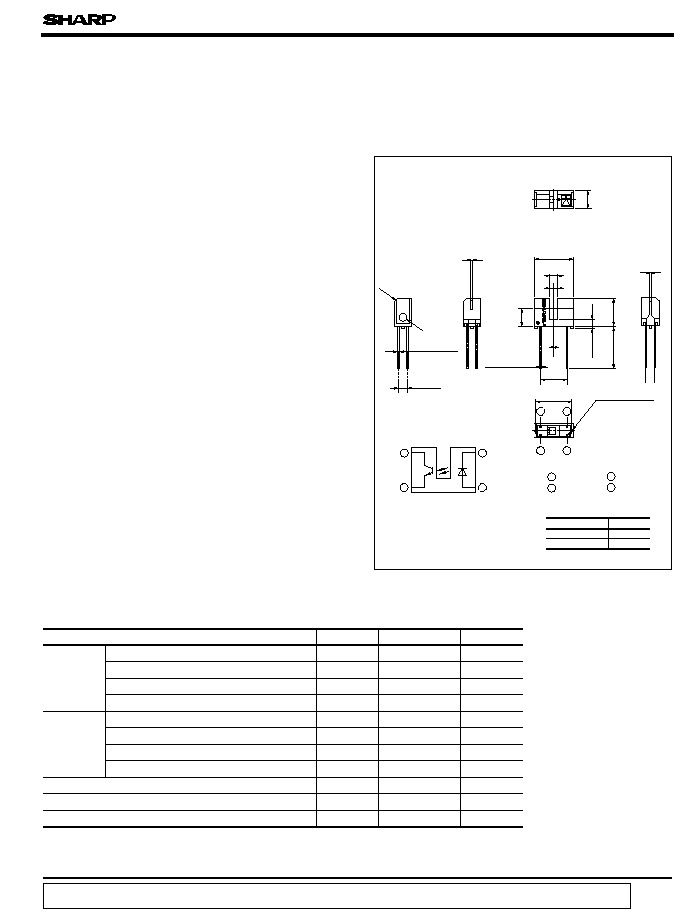
Outline Dimemsions
(Unit : mm )
GP1S55
8.0
( 5.5
)
11.0
Internal connection
diagram
( Slit width of detector side )
Detector center
B
A
A
'
B
'
2
-
0.7
2.0
5.0
(7.4)
0.5
3
4
2
1
4
1
2
3
3 Collector
4 Emitter
1 Anode
2 Cathode
( Slit width of
emitter side )
B-B
'
section
A-A
'
section
Compact, High Sensing
Accuracy Narrow Gap
Type Photointerrupter
Parameter
Symbol
Rating
Unit
Input
Forward current
50
mA
1
A
Reverse voltage
6
V
Power dissipation
75
mW
Output
Collector-emitter voltage
35
V
Emitter-collector voltage
6
V
Collector current
20
mA
Collector power dissipation
75
mW
Operating temperature
- 25 to + 85
∞C
Storage temperature
- 40 to + 100
∞C
260
∞C
Dimensions(d) Tolerance
d
<=
6.0
±
0.1
6.0
<
d
<=
18.0
±
0.2
*1
Peak forward current
*2
Soldering temperature
I
F
I
FM
V
R
P
V
CEO
V
ECO
I
C
P
C
T
opr
T
stg
T
sol
2. VCRs , cassette decks
1. Compact package ( Case height: 8mm )
2. High sensing accuracy
1. OA equipment such as FDDs. printers,
facsimiles
( Slit width∑∑∑ Detector side: 0.15mm,
Emitter side: 0.5mm )
3. Easy positioning to PWB with positioning
pin
4. PWB direct mounting type
*
Unspecified tolerances
*
( )
:
Reference dimensions
shall be as follows
;
(2.54)
D
C1
data books, etc. Contact SHARP in order to obtain the latest version of the device specification sheets before using any SHARP's device.
"
"
In the absence of confirmation by device specification sheets, SHARP takes no responsibility for any defects that occur in equipment using any of SHARP's devices, shown in catalogs,
0.15
±
0.07
12.0
MIN.
2
-
0.7
±
0.05
10.2
±
0.15
0
-
4.5
+
0.3
-
0.1
4
-
0.4
+
0.3
-
0.1
2.0
+
0.3
-
0
GP1S55T
(Ta = 25∞C )
s
Electro-optical Characteristics
Input
Output
Transfer
charac-
teristics
- 25
0
25
50
75
85
100
0
10
20
30
40
50
60
- 25
0
25
50
75
85
100
0
20
40
60
80
100
120
75
500
200
100
50
20
5
2
5
2
5
Duty ratio
Pulse width<=100
µ
s
0
0.5
1
1.5
2
2.5
3
1
2
5
10
20
50
100
200
500
25∞C
0∞C
50∞C
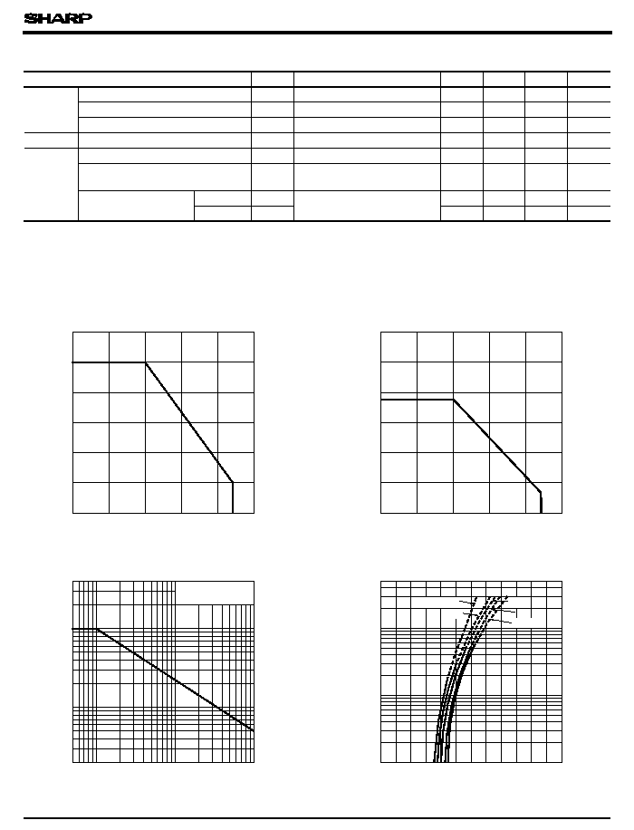
Fig. 1 Forward Current vs.
Ambient Temperature
Fig. 2 Collector Power Dissipation vs.
Ambient Temperature
Forward voltage V
F
Ambient temperature T
a
Ambient temperature T
a
T
a
= 25∞C
T
a
= 75∞C
Fig. 3 Peak Forward Current vs.
Duty Ratio
Fig. 4 Forward Current vs.
Forward Voltage
- 25∞C
Conditions
MIN.
TYP.
MAX.
Unit
Forward voltage
-
1.2
1.4
V
Peak forward voltage
-
3
4
V
Reverse current
-
-
10
µ
A
Collector dark current
-
0.6
-
-
mA
Collector-emitter saturation
voltage
-
-
0.4
V
Response time
Rise time
-
5
25
µ
s
Fall time
-
6
30
µ
s
Parameter
I
F
=20mA
I
FM
=0.5A
V
R
=3V
V
CE
=20V
1
F
= 20mA, V
CE
= 5V
V
CE
= 2V, I
C
= 2mA
R
L
= 100
I
F
= 40mA, I
C
= 0.6mA
Symbol
V
F
V
FM
I
R
I
CEO
V
CE ( sat )
t
r
t
r
Forward current I
F
(
mA
)
Collector power dissipation Pc
(
mW
)
Forward current I
F
(
mA
)
10
- 2
10
- 1
(V)
1
100
nA
(∞C)
Peak forward current I
FM
(
mA
)
10
0
(∞C)
2000
1000
Collector Current
Ic

10
20
30
40
50
0
0
1
2
4
5
3
0
25
- 25
0
1
2
50
100
75
0.01
0.1
0.1
1
10
0.2
0.5
1
2
5
10
20
50
100
1
2
3
4
5
0
0
1
2
3
4
5
6
6
10
9
8
7
0
25
- 25
0.15
0.20
Collector-emitter saturation voltage
50
100
75
Output
Output
Input
10%
90%
V
CE
= 5V
Fig. 6 Collector Current vs.
Collector-emitter Voltage
I
F
= 20mA
V
CE
= 5V
I
F
= 40mA
I
C
= 0.6mA
Fig. 8 Collector-emitter Saturation Voltage vs.
Ambient Temperature
V
CE
= 2V
I
C
R
L
t
d
t
r
t
s
Input R
D
Forward current I
F
Collector-emitter voltage V
CE
I
F
L
t
f
t
r
t
d
t
s
T
a
= 25∞C
T
a
= 25∞C
Ambient temperature T
a
Ambient temperature T
a
T
a
= 25∞C
t
f
Fig. 5 Collector Current vs.
Forward Current
Fig. 7 Collector Current vs.
Ambient Temperature
Fig. 9 Response Time vs.
GP1S55T
8
Collector current Ic
(mA
)
( mA )
Collector current Ic
(mA
)
( V)
= 50mA
40mA
30mA
20mA
10mA
V
CE
(
sat
)
(
V
)
0.10
Collector current Ic
(mA
)
(∞C)
Response time
(
µ
s
)
Test Circuit for Response Time
V
CC
( k
)
= 2mA
(∞C)
Load Resistance
Load resistance R

2
5
- 20
- 15
- 10
- 5
0
5
5
5
Fig.10 Frequency Response
2
2
2
10k
1k
100
- 25
0
25
100
50
75
2
5
2
5
2
5
2
5
0
50
100
- 0.4 - 0.3 - 0.2 - 0.1
0
0.1 0.2
0.3 0.4 0.5
L
0
Detector
Shield
(Detector center )
-
+
50
100
- 2
- 1
0
1
2
0
Detector
Shield
(
Detector center
)
-
+
L
V
CE
= 20V
Fig.11 Collector Dark Current vs.
Ambient Temperature
I
F
V
CE
= 5V
I
F
V
CE
= 5V
Fig.12 Relative Collector Current vs.
Shield Distance (1)
Fig.13 Relative Collector Current vs.
Shield Distance (2)
R
L
=
Ambient temperature T
a
T
a
= 25∞C
T
a
= 25∞C
GP1S55T
s
Precautions for Use
V
CE
= 2V
I
C
T
a
= 25∞C
Voltage gain Av
(
dB
)
10
3
10
4
10
5
10
6
= 2mA
10
- 6
10
- 7
10
- 8
10
- 9
10
- 10
( ∞C)
Collector dark current I
CEO
(
A
)
Shield distance L ( mm )
- 0.5
Relative collector current
(%
)
Shield distance L ( mm )
= 20mA
Relative collector current
(%
)
( 1) In case of cleaning, use only the following type of cleaning solvent.
Ethyl alcohol, methyl alcohol, isopropyl alcohol
Frequency f ( Hz )
= 20mA
( 2) As for other general cautions, refer to the chapter " Precautions for Use .
"