 | –≠–ª–µ–∫—Ç—Ä–æ–Ω–Ω—ã–π –∫–æ–º–ø–æ–Ω–µ–Ω—Ç: GP2W0001 | –°–∫–∞—á–∞—Ç—å:  PDF PDF  ZIP ZIP |
IrDA Data Sheet
1
GP2W0001YP
IrDA Data Sheet
115 kbps Transceiver
FEATURES
∑ Built-in Photodiode
∑ Operating voltage 2.7 V to 5.5 V
∑ In circuit design, allow for the degradation of light
emitting diode output that results from long continu-
ous operation (50% degradation/5 years).
∑ This product shall not contain the following materi-
als, and these materials shall not be used in the pro-
duction process for this product.
≠ CFCs
≠ Halon
≠ Carbon Tetrachloride
≠ 1.1.1. Trichloroethane (Methylchloroform)
≠ Specific brominated flame retardants such as the
PBBOs and PBBs are not used in this device.
INTRODUCTION
This specification applies to the outline and charac-
teristics of IrDA 1.2 type (data rate 2.4 kbps to
115.2 kbps, low power option compliant) optical data
communication transceiver.
NOTES
∑ Caution should be taken to prevent the detector sur-
face from being smeared with dust or dirt, or from
being touched, as it may cause faulty operation.
∑ Cleaning conditions:
≠ Solvent cleaning: Solvent temperature 45∞C or
less. Immersion for 3 minutes or less.
≠ Ultrasonic cleaning: The effect of ultrasonic
cleaning on the device differs by cleaning bath
size, ultrasonic power output, cleaning time, PCB
size or device mounting condition, etc. Test the
device under actual conditions and confirm that
ultrasonic cleaning does not cause any immedi-
ate or potential defects.
≠ Cleaning solvent: The cleaning shall be carried
out with ethyl alcohol, methyl alcohol, or isopropyl
alcohol.
∑ In order to prevent electrostatic damage to the inte-
grated circuit, handle this device in a static-free envi-
ronment and workstation.
∑ External force applied to the device after mounting can
cause mounting defects such as the terminal coming
off. Be careful when handling the device and prevent
objects from touching the device after mounting.
∑ Refer to the `Precautions for Soldering' section.
∑ When the system (program) is designed, the turn
around time from transmit to receive should be
designed by considering 0.5 ms or more that is spec-
ified by IrDA. This turn around time means the time
that this device temporarily does not detect the
incoming signal, since the transmitted light from the
transmitter side reaches the detector side of the
same transceiver.
∑ Consider that 20 ms or more (at T
A
= 25∞C, no input
signal) is necessary to return from shut-down mode
to ready operation mode. In addition, thoroughly
confirm the operation in the actual application.
∑ When there is considerable external stray light or a
light source is located near the transceiver, or the
detector face receives considerable external stray
light, a pulse other than the desired signal output may
be generated as noise on the output terminal of the
transceiver. Consider the layout and structure in your
design to minimize disturbing light on the detector face.
∑ When the sensor is adopted in an IR communication
system, it should be used according to the signal
method specified by `Serial Infrared Physical Layer
Link Specification' published by the Infrared Data
Association. Faulty operation may occur if a signal
method other than that specified is used.
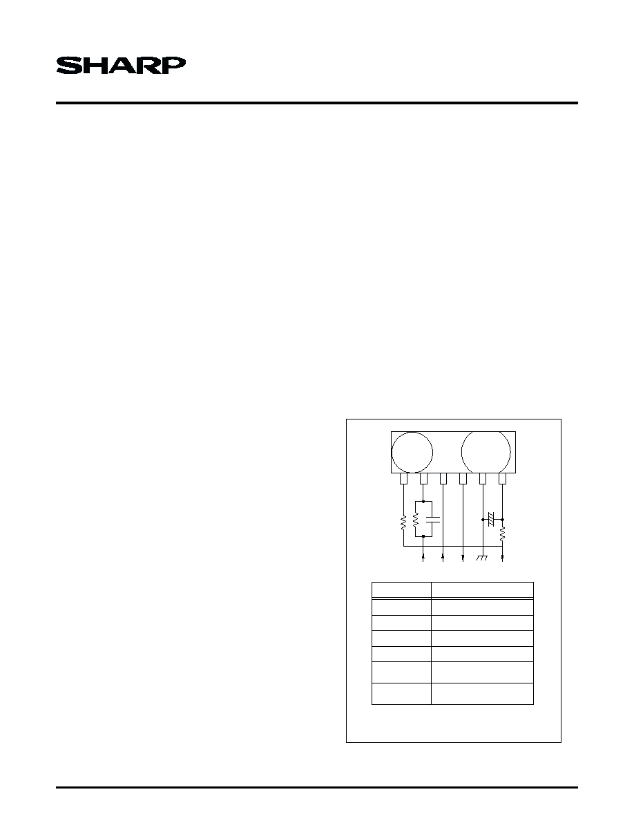
Figure 1. Recommended External Circuit
1
LEDA
RL
R
2
CX
2
CX
1
R
1
2
TXD
3
SD
SD
TX
4
RXD
RXD
GP2W0001YP-1
5
GND
6
V
CC
V
CC
+
COMPONENTS
NOTE: Choose the most suitable CX
1
and R
1
according to
the noise level and noise frequency of power supply.
RECOMMENDED VALUES
CX
1
CX
2
R
1
R
2
47
µF/6.3 V (NOTE)
RL
(STANDARD)
RL
(LOW POWER)
1500 pF/25 V
47
±5%, 1/10 W (NOTE)
1 k
±5%, 1/10 W
2.2
±5%, 1/2 W
(V
CC
= 3.0 V, I
E
= 40 mW/sr)
33
±1%, 1/8 W
(V
CC
= 3.0 V, I
E
= 3.6 mW/Sr)

GP2W0001YP
115 kbps Transceiver
2
IrDA Data Sheet
Figure 2. System Example
+
GP2W0001YP-2
UART
ENCODER
CIRCUIT
DECODER
CIRCUIT
GP2W0001YP
3
3
TXD
CX
2
GND
4
2
1
5
RXD
SD
LEDA
CX
1
R
1
RL
V
CC
R
2
SD INPUT
PERFORMANCE
HIGH
Normal Mode
LOW or
OPEN
Shutdown
Mode
NOTES:
1 Transmitting data waveform
2 Encoder circuit output waveform
3 Transmitter output optical signal waveform
4 GP2W0001YP receiver output waveform
5 Receiving data waveform

115 kbps Transceiver
GP2W0001YP
IrDA Data Sheet
3
Recommended Size of
Solder Cream Paste
Open the solder mask as shown in Figure 4. The size
of solder cream paste for this device before reflow sol-
dering must be as large as the foot pattern landings.
Figure 3. Signal Waveform Example
NOTES:
1 Transmitting data waveform
2 Encoder circuit output waveform
3 Transmitter output optical signal waveform
4 GP2W0001YP receiver output waveform
5 Receiving data waveform
1
Data Rate
T =
Data rate: 2.4 kbps, 9.6 kbps, 19.2 kbps, 38.4 kbps,
57.6 kbps, 115.2 kbps
0
0
T
3T/16
1
0
1
T
3
1
2
4
5
1
0
1
GP2W0001YP-3
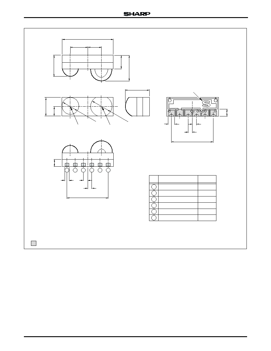
Figure 4. Foot Pattern and
Solder Cream Paste Size
0.9
0.7
P 1.4 x 5 = 7
1.7
1
2
3
4
5
6
LED Anode
Transmitter Data Input
Shutdown
Receiver Data Output
Ground
Supply Voltage
LEDA
PIN
PIN NAME
SYMBOL
TXD
SD
RXD
GND
V
CC
1
2
3
4
5
6
0.9
0.7
P 1.4 x 5 = 7
1.7
NOTES: Dimensions are in mm.
GP2W0001YP-4
1
2
3
4
5
6
Soldering paste area
View from parts side
LENS (PD/LED) SIDE
Solder Mask Opening
GP2W0001YP
115 kbps Transceiver
4
IrDA Data Sheet
Figure 5. GP2W0001YP Outline Dimensions
2.95
4.2
8.7
±0.2
2.325
3.5
3.15
1.7
0.6
2.2
4.2
0.7
0.7
P 1.4 x 5 = 7
±0.2
1
6 - 0.8
+0.2
-0.3
0.7
1.0
EMBOSSED
'S'
0.7
P 1.4 x 5 = 7
±0.2
6 - 1.1
±0.2
2
3
5
6
4
CENTER
OF DETECTOR
CENTER
OF EMITTER
2.8
±0.1
3.6
±0.1
NOTES:
1. Dimensions are in mm.
2. Unspecified tolerances are ±0.3 mm.
3. Adhesion of resin to the terminal area are allowed MAX. 0.3 mm.
4. Resin burr are not included in this outline drawing.
5. Product mass: Approx. 0.12 g
6. Mold resin: Epoxy resin (black)
area: Au plating
GP2W0001YP-5
1
2
3
4
5
6
LED Anode
Transmitter data Input
Shutdown
Receiver Data Output
Ground
Supply Voltage
LEDA
PIN
PIN NAME
SYMBOL
TXD
SD
RXD
GND
V
CC

115 kbps Transceiver
GP2W0001YP
IrDA Data Sheet
5
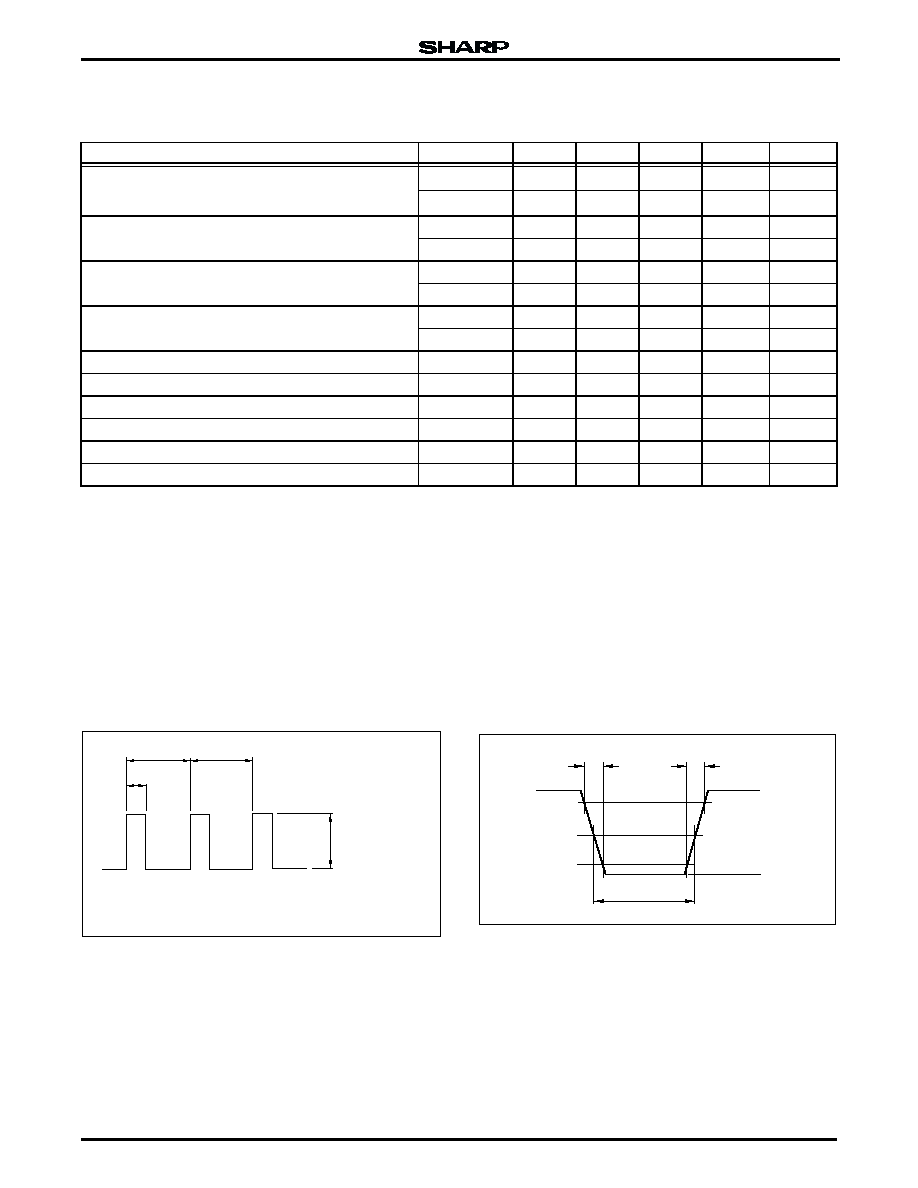
RATINGS AND CHARACTERISTICS
Absolute Maximum Ratings
NOTES:
1. Pulse width: 78.1 µs. Duty ratio: 3/16.
2. Soldering reflow time: 5 seconds.
Recommended Operating Conditions
NOTES: *Recommended circuit of emitter side.
PARAMETER
SYMBOL
RATINGS
UNIT
NOTES
Supply voltage
V
CC
0 to 6.0
V
Forward current
I
F
50
mA
Peak forward current
I
FM
500
mA
1
Operating temperature
T
OPR
-10 to +70
∞C
Storage temperature
T
STG
-20 to +85
∞C
Soldering temperature
T
SOL
230
∞C
2
PARAMETER
SYMBOL
OPERATING CONDITION
UNIT
Supply voltage
V
CC
2.7 to 5.5
V
Data rate
BR
2.4 to 115.2
kbps
Shutdown circuit high level input voltage
V
IHSD
V
CC
≠ 0.6 to V
CC
V
Shutdown circuit low level input voltage
V
ILSD
0.0 to 0.4 or Open
V
Logic high transmitter input voltage*
V
IHTXD
2.4 to V
CC
V
Logic low receiver input voltage*
V
ILTXD
0.0 to 0.4
V
GP2W0001YP
115 kbps Transceiver
6
IrDA Data Sheet
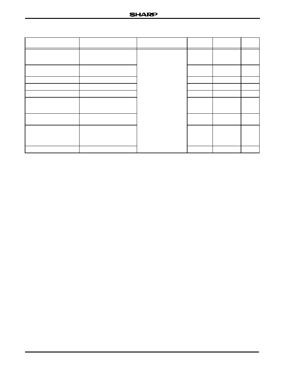
Electrical Characteristics
T
A
= -25∞C, V
CC
= 5 V unless otherwise specified
NOTES:
1. V
CC
= 5 V, no input signal, output terminal open, V
IHSD
= V
CC
-0.6 V.
2. V
CC
= 3 V, no input signal, output terminal open, V
IHSD
= V
CC
-0.6 V.
3. V
CC
= 5 V, SD terminal open.
4. V
CC
= 3 V, SD terminal open.
5. V
CC
= 5 V.
6. V
CC
= 3 V.
7. V
CC
= 5 V, I
OL
= 400 µA.
8. V
CC
= 3 V, I
OL
= 400 µA. See Figures 6, 7, and 8.
9. BR = 115.2 kbps. See Figures 6, 7, and 8.
10. V
OH
, V
OL
, tw, tr, tf shall be satisfied at
15∞. See Figures 6, 7, and 8.
11. BR = 115.2 kbps,
15∞, V
CC
= 3 V, RL = 2.2
,
VINTX = 2.7 V, R2 = 1 k
±5%, CX2 = 1,500 pF. See Figures 9, 10, and 11.
PARAMETER
SYMBOL
MIN.
TYP.
MAX.
UNIT
NOTES
Current consumption at no input signal
I
CC1
1.0
1.4
mA
1
I
CC2
0.7
1.0
mA
2
Current consumption at shut-down mode
I
CC1-S
0.5
1.0
µA
3
I
CC2-S
0.3
1.0
µA
4
High level output voltage
V
OH1
4.5
V
5
V
OH2
2.5
V
6
Low level output voltage
V
OL1
0.6
V
7
V
OL2
0.6
V
8
Low level pulse width
tw
0.8
8.0
µs
9
Rise time
tr
1.2
µs
9
Fall time
tf
0.2
µs
9
Maximum reception distance
L
1
m
10
Radiant intensity
I
E
40
350
mW/Sr
11
Peak emission wavelength
p
850
870
900
nm
11
Figure 6. Input Signal Waveform (Detector Side)
NOTE: At BR = 2.4 kbps: T
1
= 416.7 µs, T
2
= 78.1 µs
At BR = 115.2 kbps: T
1
= 8.68 µs, T
2
= 1.63 µs
T
1
T
2
RADIATION
INTENSITY OF
TRANSMITTER
40 mW/Sr
T
1
GP2W0001YP-6
Figure 7. Output Waveform (Detector Side)
t
W
V
OL
t
R
t
F
V
OH
90%
50%
10%
GP2W0001YP-7

115 kbps Transceiver
GP2W0001YP
IrDA Data Sheet
7
Figure 8. Standard Optical System (Detector Side)
L
GP2W0001YP-8
TRANSMITTER
(NOTE 1)
OSCILLOSCOPE
GP2W0001YP
NOTES:
1. Transmitter uses GP2W0001YP (
p = 870 nm TYP.)
adjusted to a radiation intensity of 40 mW/Sr.
2.
Indicates horizontal and vertical directions.
3. Ee: Detector face illuminance < 10 x
Figure 9. Output Waveform Specification
(Emitter Side)
t
R
t
F
90%
10%
I
E
GP2W0001YP-9

GP2W0001YP
115 kbps Transceiver
8
IrDA Data Sheet
Figure 10. Standard Optical System (Emitter Side)
GP2W0001YP-10
DETECTOR FOR
RADIATION INTENSITY
MEASURMENT
GP2W0001YP
NOTE:
indicates horizontal
and vertical directions
Figure 11. Recommended Circuit (Emitter Side)
1.63
µs
V
IN
Tx = 2.7 V
GP2W0001YP
TX
TXD
CX
2
= 1500 pF
LEDA
V
CC
= 3 V,
RL = 2.2
R
2
= 1 k
BR = 115.2 kbps
GP2W0001YP-11
Figure 12. Peak Forward Current
Versus Ambient Temperature
GP2W0001YP-12
PEAK
FORWARD
CURRENT
I
FM
(mA)
300
400
200
100
-10
60 70
100
75
50
25
AMBIENT TEMPERATURE T
A
(
∞C)
0
-25
0
115 kbps Transceiver
GP2W0001YP
IrDA Data Sheet
9
RELIABILITY
1
NOTES:
1. Confidence level 90%, LTPD 10%/20%.
2. The sample to be tested shall be left at normal temperature and humidity for
2 hours after it is taken out of the chamber. No dew point.
3. Refer to the `Precautions for Soldering' section for temperature profile.
TEST ITEMS
TEST CONDITIONS
FAILURE JUDGEMENT
CRITERIA
SAMPLES
(n)
DEFECTIVE
(c)
NOTES
Temperature cycling
1 cycle -20∞C to 85∞C
(30 minutes at each extreme)
20 cycles test
I
CC1
> Up ◊ 1.2
I
CC2
> Up ◊ 1.2
L < Low ◊ 0.8
Judgement of Criteria:
V
OH1
< Low ◊ 0.8
V
OH2
< Low ◊ 0.8
V
OL1
> Up ◊ 1.2
V
OL2
> Up ◊ 1.2
tw
1
> Up ◊ 1.2
tw
1
< Low ◊ 0.8
tw
2
> Up ◊ 1.2
tw
2
< Low ◊ 0.8
tr > Up ◊ 1.2
tf > Up ◊ 1.2
Up: Upper
Specification Limit
Low: Lower
Specification Limit
n = 22
c = 0
2
High temperature and high
humidity storage
+40∞C, 90% RH, 240 hours
n = 22
c = 0
2
High temperature storage
+85∞C, 240 hours
n = 22
c = 0
2
Low temperature storage
-20∞C, 240 hours
n = 22
c = 0
2
Operation life 1
+25∞C, V
CC
= 5 V, 240 hours
n = 11
c = 0
2
Operation life 2
+25∞C, I
FM
= 400 mA,
240 hours, Pulse width
78.1 µs, Duty ratio 3/16
n = 11
c = 0
Mechanical shock
1,000 m/s
2
, 6 ms,
3 times/±X, ±Y, ±Z direction
n = 11
c = 0
Variable frequency
vibration
200 m/s
2
,
100 to 2,000 to 100 Hz for
approximately 4 minutes
48 minutes/X, Y, Z direction
n = 11
c = 0
Reflow solder heat
230∞C, 5 s.
n = 11
c = 0
3
GP2W0001YP
115 kbps Transceiver
10
IrDA Data Sheet
INCOMING INSPECTION
∑ Inspection lot: Inspection shall be carried out per
each delivery lot.
∑ Inspection method: A single sampling plan, normal
inspection level two based on ISO 2859 shall be
adopted.
PRECAUTIONS FOR SOLDERING
Solder Reflow
Solder only once at the temperature and the time
within the temperature profile as shown in Figure 13.
Other Precautions
An infrared lamp used to heat up for soldering may
cause a localized temperature rise in the resin. Keep the
package temperature within that specified in Figure 13.
Also avoid immersing the resin part in the solder. Even if
within the temperature profile shown in Figure 13, there
is the possibility that the gold wire in the package may
break if the deformation of the PCB affects the lead pins.
Use after fully confirming the conditions of actual solder
reflow machine.
Soldering
∑ Soldering iron shall be less than 25 W, and temper-
ature of soldering iron point shall be used at less
than 260∞C.
∑ Soldering time shall be within 3 seconds.
∑ Soldered product shall treat at normal temperature.
∑ Solder: 6/4 solder or included Ag solder.
Table 1. Incoming Inspection
PARAMETER
INSPECTION ITEMS AND
TEST METHOD
AQL(%)
Major defect
Disconnection, short
0.1
Inverse polarity on terminal
0.1
Soldering defect (obstacle
to use)
0.1
Electrical characteristic defect
0.1
Minor defect
Appearance defect which
affects the electrical character-
istics such as, split, chip,
scratch, stain, or blur
0.25
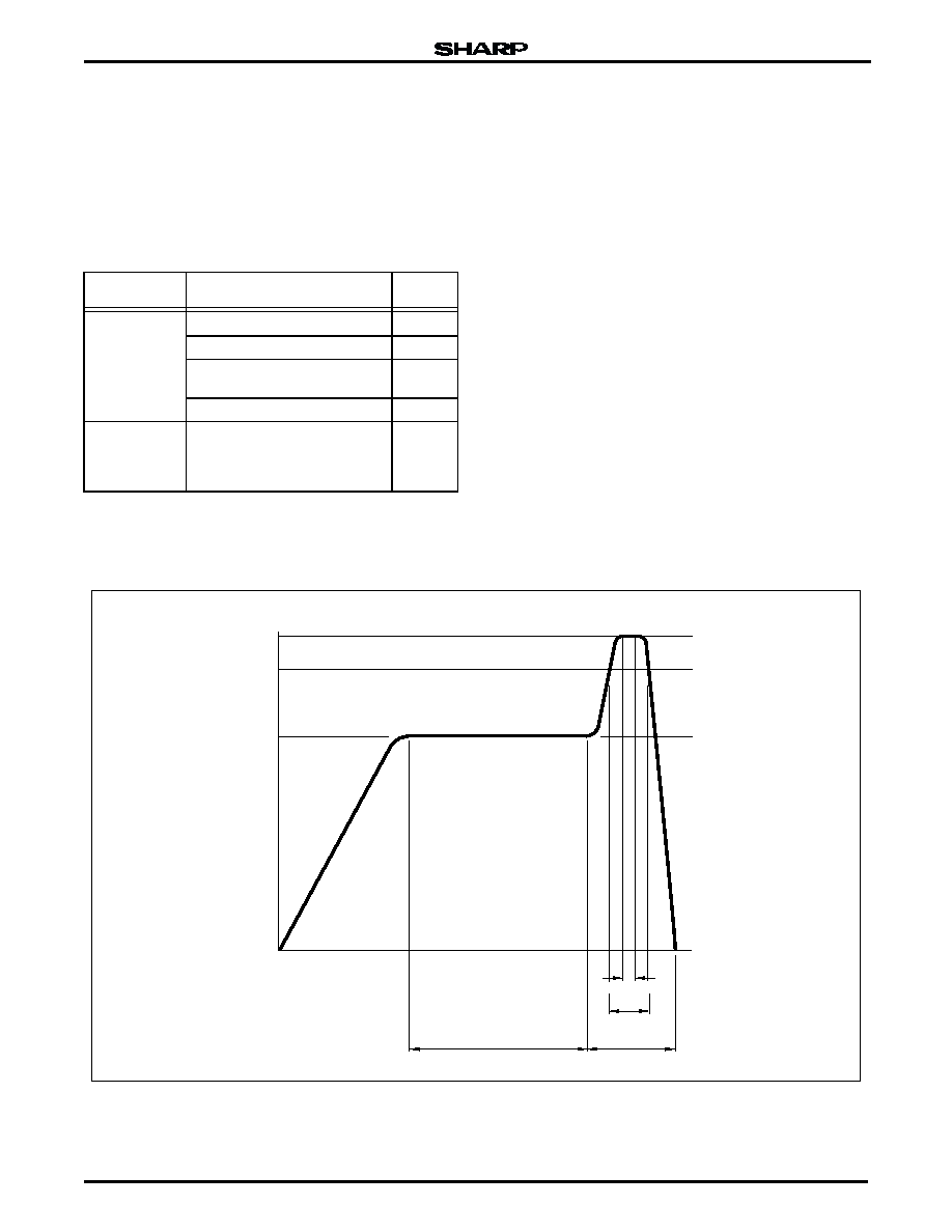
Figure 13. Temperature Profile
1 - 4
∞C/s
200
∞C
230
∞C
MAX.
165
∞C
MAX.
25
∞C
120 s MAX.
90 s MAX.
60 s MAX.
5 s MAX.
1 - 4
∞C/s
1 - 4
∞C/s
GP2W0001YP-13
115 kbps Transceiver
GP2W0001YP
IrDA Data Sheet
11
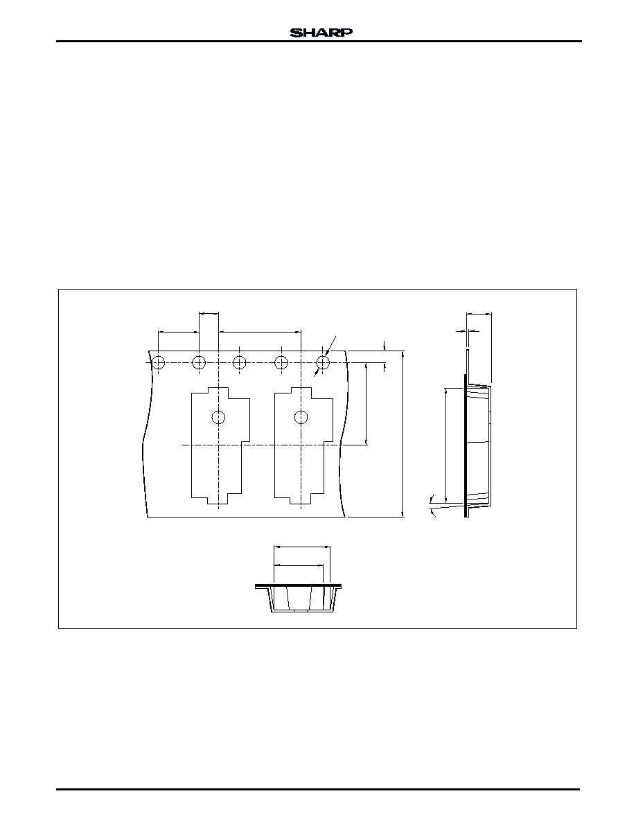
TAPING SPECIFICATIONS
Taping Method
∑ Taping structure and dimensions: The tape should
have a structure in which a cover tape is sealed by
using heat-pressed on the carrier tape of conductive
PET. See Figure 14.
∑ Reel structure and dimensions: The taping reel
should be conductive plastic with its dimensions as
shown in Figure 15.
∑ Direction of product insertion: Product direction in
carrier tape should be such that electrode side of
product is placed on the cover tape side and lens
side of product is placed on the hold side of the tape.
See Figure 16.
∑ Taped device repair: To repair taped device failure,
cut the bottom of carrier tape with a cutter, and after
replacing with good devices, seal the cut portion with
adhesive tape.
∑ Adhesiveness of cover tape: The exfoliation force
between carrier tape and cover tape should be 0.2 N
to 1 N for the angle from 160∞ to 180∞.
∑ Rolling method and quantity: Wind the tape back on
the reel so that the cover tape is on the outside.
Attach more than 20 cm of blank tape to the trailer
and the leader of the tape and fix both ends with
adhesive tape. One reel shall contain 2,000 pieces.
∑ Safety protection during shipping: There should be
no deformation of component or degradation of elec-
trical characteristics due to shipping.
Figure 14. Tape Structure and Dimensions
4.0
±0.1
2.0
±0.1
8.0
±0.1
4.8
±0.25
3.5
±0.1
0.3
±0.05
7.5
±
0.1
1.75
±
0.1
10.7
±
0.1
16.0
±
0.3
4.1
±0.25
1.5
+0.1
-0.0
7
∞ MAX.
GP2W0001YP-14
NOTE:
Dimensions are in mm.

GP2W0001YP
115 kbps Transceiver
12
IrDA Data Sheet
Figure 15. Reel Structure and Dimensions
Figure 16. Direction of Product Insertion
330
±2
13
±0.2
2
±0.5
22.4 MAX.
21
±0.8
17.5
±0.5
100
±
0.1
GP2W0001YP-15
NOTE:
Dimensions are in mm.
GP2W0001YP-16
LENS
SIDE
PULL-OUT DIRECTION
115 kbps Transceiver
GP2W0001YP
IrDA Data Sheet
13
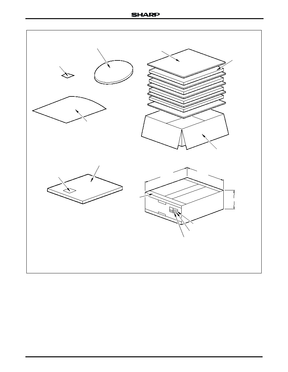
TAPING MOISTURE-PROOF PACKING
Packaging Specifications
Packaging Method
∑ Seal the aluminum laminated bag containing the
tape reel (2,000 pieces per reel) and desiccant.
∑ Fill out necessary information on the label and paste
it on the aluminum laminate bag.
∑ Pack four aluminum laminated bags (containing one
reel each) into the designated outer case, where
paper pads are placed on the bottom and top of the
outer case, as well as between each layer of the alu-
minum laminated bags. Minimum order/shipment
quantity should be one laminated bag.
∑ The outer case should then be sealed with packing
tape, indicating the model name, quantity, and out-
going inspection data on the case. Total of 8,000
pieces per carton.
Storage and Treatment After Unsealing
∑ Storage conditions: The product should be stored
with these conditions:
≠ Storage temperature: 10∞C to 30∞C
≠ Humidity: below 60% RH
∑ Treatment after opening:
≠ After unsealing, devices should be mounted un-
der the temperature condition of 10∞C to 30∞C, at
the humidity conditions of below 60% RH, within
two days.
≠ In case long term storage is needed, devices
should either be stored in dry box or re-sealed in
a moisture-proof bag with desiccant and kept in
an environment where the temperature is 10∞C to
30∞C, at the humidity condition of below 60% RH.
Devices must be mounted within two weeks.
∑ Baking before mounting:
≠ In the event that the devices are not maintained
in the recommended storage conditions or the
enclosed desiccant indicator has turned pink,
baking must be done before devices are mount-
ed. Please also note that baking should only be
done once.
≠ Recommended condition: 100∞C, 12 to 24 hours.
≠ Baking will not be properly done with the devices
in their shipping package. To complete the baking
properly, devices should either be temporarily
mounted to PCB with adhesive, or placed in a
metal tray. The temporary mounting should be
done using adhesive, not by soldering.
Table 2. Packaging Material
NAME
MATERIAL
Aluminum laminate bag
Aluminum polyethylene
Label
Paper
Desiccant
Outer case
Paper
Pads
Paper
Table 3. Packaging Method Specifications
PACKAGE
SHAPE
PRODUCT
QUANTITY
SACK
QUANTITY
Tape reel
(
330 mm)
1 model
2,000
pieces
per reel
1 reel per
moisture-proof
laminated bag
GP2W0001YP
115 kbps Transceiver
14
IrDA Data Sheet
Figure 17. Packing Specification
GP2W0001YP-17
PADS
(TOTAL 5 SHEETS)
PRODUCTS
IN TAPE-REEL
DESICCANT
LABEL
(MODEL NUMBER
QUANTITY
DATE)
PACKAGE METHOD EXAMPLES:
1. Seal the aluminum laminated bag, including the tape reel
with 2,000 pieces and desiccant.
2. Fill out the model name, quantity etc. in the blank area of label
and paste on the bag.
3. Put the four moisture-proof laminated bags in the ruled case.
Put the pad between the bags, and top and bottom.
4. Seal the case with packing tape, and indicate model name
and quantity. (8,000 pieces/package)
Total Packaged mass: Approximately 3.6 kg.
TAPE-REEL IN
ALUMINUM LAMINATED BAG
PACKING CASE
ALUMINUM
LAMINATED BAG
MODEL NUMBER
440 mm TYP.
PACKING
TAPE
EXAMPLE 1
EXAMPLE 3
EXAMPLE 4
EXAMPLE 2
370 mm TYP.
150 mm TYP.
QUANTITY
DATE
TAPE-REEL IN
ALUMINUM
LAMINATED BAG
(TOTAL 4 SETS)
NOTE:
Dimensions are in mm.

115 kbps Transceiver
GP2W0001YP
©2000 by SHARP Corporation
Reference Code SMA00011
NORTH AMERICA
EUROPE
ASIA
SHARP Microelectronics
of the Americas
5700 NW Pacific Rim Blvd.
Camas, WA 98607, U.S.A.
Phone: (360) 834-2500
Telex: 49608472 (SHARPCAM)
Facsimile: (360) 834-8903
http://www.sharpsma.com
SHARP Electronics (Europe) GmbH
Microelectronics Division
Sonninstraþe 3
20097 Hamburg, Germany
Phone: (49) 40 2376-2286
Facsimile: (49) 40 2376-2232
http://www.sharpmed.com
LIFE SUPPORT POLICY
SHARP components should not be used in medical devices with life support functions or in safety equipment (or similiar applications where
component failure would result in loss of life or physical harm) without the written approval of an officer of the SHARP Corporation.
LIMITED WARRANTY
SHARP warrants to its Customer that the Products will be free from defects in material and workmanship under normal use and service for a
period of one year from the date of invoice. Customer's exclusive remedy for breach of this warranty is that SHARP will either (i) repair or
replace, at its option, any Product which fails during the warranty period because of such defect (if Customer promptly reported the failure to
SHARP in writing) or, (ii) if SHARP is unable to repair or replace, refund the purchase price of the Product upon its return to SHARP. This
warranty does not apply to any Product which has been subjected to misuse, abnormal service or handling, or which has been altered or
modified in design or construction, or which has been serviced or repaired by anyone other than Sharp. The warranties set forth herein are in
lieu of, and exclusive of, all other warranties, express or implied. ALL EXPRESS AND IMPLIED WARRANTIES, INCLUDING THE
WARRANTIES OF MERCHANTABILITY, FITNESS FOR USE AND FITNESS FOR A PARTICULAR PURPOSE, ARE SPECIFICALLY
EXCLUDED. In no event will Sharp be liable, or in any way responsible, for any incidental or consequential economic or property damage.
The above warranty is also extended to Customers of Sharp authorized distributors with the following exception: reports of failures of Products
during the warranty period and return of Products that were purchased from an authorized distributor must be made through the distributor.
In case Sharp is unable to repair or replace such Products, refunds will be issued to the distributor in the amount of distributor cost.
SHARP reserves the right to make changes in specifications at any time and without notice. SHARP does not assume any responsibility
for the use of any circuitry described; no circuit patent licenses are implied.
SHARP Corporation
Integrated Circuits Group
2613-1 Ichinomoto-Cho
Tenri-City, Nara, 632, Japan
Phone: +81-743-65-1321
Facsimile: +81-743-65-1532
http://www.sharp.co.jp