
GP2W1002YP
GP2W1002YP
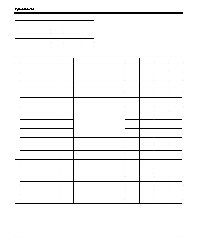
I Absolute Maximum Ratings
I Outline Dimensions
(Unit : mm)
Low Profile Type IrDA Transceiver
Module Compliant with IrDA1.1
1. Personal computers.
2. Personal information tools.
3. Cellular phone.
I Features
I Applications
1. Integrated package of light emitter and receiver.
(8.0
◊3.0◊H2.5 mm)
2. Low profile type. (Height:2.5 mm)
3. Compliant with IrDA1.0 and IrDA1.1. (except 4Mbps)
4. Low voltage operation type.
(Supply voltage:2.4V to 5.5V)
5. Low dissipation current thanks to power down mode.
(Dissipation current at shut-doen mode:Max. 1
µA)
6. Applicable for reflow soldering.
7. With shield case.
Parameter
Symbol
Rating
Unit
Supply voltage
V
CC
0 to
+6.0
V
V
LED supply voltage
V
LED
0 to
+7.0
V
Transmitter data input
TXD
0 to V
CC
+0.5
Shutdown
SD
0 to V
CC
+0.5
V
Logic I/O levels
V
IO
0 to V
CC
+0.5
V
Peak forward current
*1
*2
I
FM
600
mA
Operating temperature
T
opr
-25 to +85
∞C
Storage temperature
T
stg
-25 to +85
∞C
Soldering temperature
T
sol
240
∞C
(T
a
=25∞C)
*1 Pulse operation
*2 Soldering reflow time:10s
3.0
1.02
1.18
2.5
2.55
P0.95
◊7=6.65
3.325
8-0.65
P0.95
4.0
8.0
Mounting center
Detector
Emitter
Unspecified tolerance : ±0.2mm
Au plating
6
1
2
3
4
5
6
7
8
8
7
4
1
2
3
5
Driver
Current controlled
driver
Amplifier
AGC
Logic
Receive
Detector
1
2
3
4
5
6
7
8
Terminal
Terminal name
Symbol
LEDA
LEDC
TXD
RXD
SD
V
CC
V
IO
GND
LED Anode
LED Cathode
Transmitter Data Input
Receiver Data Output
Shutdown
V
CC
Logic I/O Levels
Ground
V
CC
V
IO
RXD
LEDA
LEDC
GND
SD
TXD
Notice
In the absence of confirmation by device specification sheets, SHARP takes no responsibility for any defects that may occur in equipment using any SHARP
devices shown in catalogs, data books, etc. Contact SHARP in order to obtain the latest device specification sheets before using any SHARP device.
Internet
Internet address for Electronic Components Group http://sharp-world.com/ecg/
GP2W1002YP
I Recommended Operating Conditions
I Electro-optical Characteristics
Parameter
Symbol
Rating
Unit
Supply voltage
V
CC
Operating temperature
T
opr
Data rate
BR
2.4 to 5.5
V
V
LED supply voltage
V
LED
2.4 to 5.5
9.6 to 1 152
kbps
Logic I/O levels
V
IO
1.5 to V
CC
V
-25 to +85
∞C
(T
a
=25∞C)
Parameter
Symbol
Conditions
No input signal, V
IHSD
=V
CC
-1.2V, T
a
=25∞C
Output terminal OPEN
*3, 4, 5
I
OL
=1mA, T
a
=25∞C
*3, 4, 5
V
IO
=1.8V, I
OH
=0.3mA, T
a
=25∞C
BR=1.152Mbps,
*3, 4, 5
V
CC
=3.3V,
CL
=15pF, T
a
=25∞C
T
a
=25∞C
t
w2
, E
e2
;BR=1.152Mbps,
15∞
No input signal, V
ILSD
=0V
Output terminal OPEN, T
a
=25∞C
V
ILSD
=0V
Output terminal OPEN, T
a
=25∞C
t
w1
, E
e1
;BR=115.2kbps,
15∞
T
a
=25∞C, V
CC
=3.3V
T
a
=25∞C, V
CC
=3.3V
Shut down mode, V
CC
=2.4 to 5.5V
Normal mode, V
CC
=2.4 to 5.5V
BR=1.152Mbps, V
CC
=2.4 to 5.5V, T
a
=25∞C
V
CC
=5V, R
LED
=4.7, T
a
=25∞C,
*6, 7, 8
15∞, V
LED
=4.5 to 5.5V, R
LED
=4.7, T
a
=25∞C,
*6, 7, 8
BR=1.152Mbps,
*6, 7, 8
,
T
a
=25∞C, V
LED
=3V
LED (ON), V
CC
=2.4 to 5.5V
LED (OFF), V
CC
=2.4 to 5.5V
T
a
=25∞C, V
IHTXD
=1.6V
T
a
=25∞C, V
ILTXD
=0 to 0.6V
TXD pin stuck high
MIN.
TYP.
MAX.
Unit
Current consumption
at shut-down mode
Current consumption
at receiving
Current consumption
at no input signal
-
-
-
1.0
100
110
ns
Jitter
I
CC-S
High level output voltage
Low level output voltage
V
OH
I
CC
I
CC-R
t
f
t
w1
-
-
-
µA
-
0.01
Low level pules width
V
OL
t
r
Rise time
Fall time
-
-
-
Maximum reception distance
V
ns
-
V
IO
-0.5
V
ns
µs
cm
-
t
j
-
Input irradiance
µW/cm
2
-
V
IHSD
V
ILSD
t
l
I
isd
-
Overload irradiance
Receiver latency
µW/cm
2
500
-
mW/cm
2
-
t
w2
-
µs
-0.01
L
E
e1
E
e2
0
µA
1.6
-
LED peak current
Rise time
Fall time
V
-
-
V
-
E
e3
100
SD input current
SD terminal input voltage logic high
SD terminal input voltage logic low
I
E
Radiant intensity
p
V
IHTXD
V
ILTXD
I
IHTXD
I
ILTXD
t
OPWM
ns
100
t
r
I
LED
t
f
-
450
TXD high level input current
TXD low level input current
Maximum optical pulse width
*3 Refer to Fig.2
*4 Refer to Fig.3
*5 Refer to Fig.3
*6 Refer to Fig.4
*7 Refer to Fig.5
*8 Refer to Fig.6
mW/sr
850
870
nm
1.6
-
V
V
µA
4.0
-
500
1.0
-
µA
445
585
50
0.6
40
-
650
µA
-
V
CC
4.0
10.0
-
100
+0.01
No input signal, T
a
=25∞C, V
CC
=3.3V
t
sdw
-
-
µs
Receiver wake up time
100
V
CC
0.5
150
-
-
40
-
-
-
50
µA
-
-
8
µs
15
-
300
900
mA
-
V
CC
-
-
0.6
-
-
-
40
ns
ns
(T
a
=25 to +85∞C, V
CC
=2.4 to 3.6V Unless othewise specified)
Receiver side
Transmitter side
TXD high level input voltage
TXD low level input voltage
Peak emission wavelength
T
a
=25∞C

GP2W1002YP
I Truth Table
SD
SW TXD LED
H
L
L
L
Off
On
On
On
L
H
L
L
Off
On
Off
Off
Off
-
Off
On
Off
-
On
Off
Pull-up
Not valid
L
H
IrDA signal
No signal
Don't care
Don't care
Receiver
TR
1
TR
2
RXD
H:High
L:Low
TR
1
*RXD equivalent circuit
RXD
TR
2
*TXD equivalent circuit
TXD
SW
SW
CX
2
CX
1
CX
3
R
1
1
2
3
4
5
6
7
8
1
2
3
4
5
6
7
8
LEDA
LEDC
TXD
RXD
SD
V
CC
V
IO
GND
Components
CX
1,3
Recommended values
(Note 1) Components choose the most suitable
CX
1 to 3
according to the noise level
and noise frequency of power supply.
(Note 2) In order to guarantee 100mW/sr,
VLED is required 4.5 to 5.5V.
10
µF/16V (Note 1)
CX
2
0.47
µF(Ceramic) (Note 1)
4.7
RLED
(0.5W)
R
1
(0.125W)
4.7
V
LED
=2.4 to 5.5V
V
CC
V
LED
NC
RLED
(Note 2)
Fig.1
Recommended External Circuit
Fig.2 Output Waveform Specification (Detector side)
t
f
t
w
t
r
90%
50%
10%
V
OH
V
OL

GP2W1002YP
t
f
t
r
90%
10%
I
E
Fig.4 Output Waveform Specification (Transmitter side)
Transmitter
1)
L
E
e
: Light detector face illuminance
<10 lx
: Indicates horizontal and vertical directions.
GP2W1002YP
Oscilloscope
1) Transmitter shall use GP2W1002YP (
p=870nm TYP.) which is
adjusted the radiation intensity at 40mW/sr (at 115.2kbps),
100mW/sr (at 1.152Mbps)
T
1
T
1
Radiantion intensity
of transmitter 40mW/sr
(at BR
=115.2kbps),
100mW/sr (at BR
=1.152Mbps)
Input signal waveform (Detector side)
At BR
=115.2kbps:T
1
=8.68µs, T
2
=1.41 to 2.23µs
At BR
=1.152Mbps:T
1
=868ns, T
2
=217ns
T
2
Fig.3 Standard Optical System (Detector side)
Fig.5 Standard Optical System (Transmitter side)
: Indicates horizontal and vertical directions.
GP2W1002YP
Detector for
radiant intensity measuring

GP2W1002YP
1.63
µs (at 115.2kbps)
217ns (at 1.152Mbps)
V
IHTXD
=2.8V
BR
=115.2kbps
BR
=1.152Mbps
TXD
V
CC
=3.3V
V
LED
=5V
4.7
GP2W1002YP
Fig.6 Recommended Circuit of Transmitter side
Fig.7 Recommended PCB Foot Pattern
2.05
1.25
0.1
1.75
1.35
0.6
0.475
1.425
3.325
1
2
3
4
5
6
7
8
Dimensions in parenthesis are shown for reference.
Terminal
Terminal name
Symbol
LEDA
LEDC
TXD
RXD
SD
V
CC
V
IO
GND
LED anode
LED cathode
Transmitter data input
Receiver data output
Shutdown
V
CC
Logic I/O levels
Ground
1
2
3
4
5
6
7
8
(unit : mm)
: Solder paste area
Please open the solder mask as below
so that the size of solder creamed paste
for this device before reflow soldering
must be as large as one of the foot
pattern land indicated at Fig.7
2.05
1.25
0.1
1.75
1.35
0.6
0.475
1.425
3.325
Mounting center
Dimensions in parenthesis are shown for reference.
(unit : mm)
Fig.8 Recommended Size of Solder Creamed Paste (Reference)