
LH28F008SA
1
8M (1M ◊ 8) Flash Memory
Figure 1. 40-Pin TSOP Configuration
FEATURES
∑
Very High-Performance Read
≠ 85 ns Maximum Access Time
∑
High-Density Symmetrically Blocked
Architecture
≠ Sixteen 64K Blocks
∑
Extended Cycling Capability
≠ 100,000 Block Erase Cycles
≠ 1.6 Million Block Erase Cycles per Chip
∑
Automated Byte Write and Block Erase
≠ Command User Interface
≠ Status Register
∑
System Performance Enhancements
≠ RY
ª
/BY
ª
Status Output
≠ Erase Suspend Capability
∑
Deep-Powerdown Mode
≠ 0.20 µA I
CC
Typical
∑
SRAM-Compatible Write Interface
∑
Hardware Data Protection Feature
≠ Erase/Write Lockout during
Power Transitions
∑
Independent Software Vendor Support
≠ Microsoft Flash File SystemTM (FFS)
∑
ETOXTM Nonvolatile Flash Technology
≠ 12 V Byte Write/Block Erase
∑
Industry Standard Packaging
≠ 40-Pin 1.2 mm ◊ 10 mm ◊ 20 mm
TSOP (Type I) Package
≠ 44-Pin 600-mil SOP Package
28F008SA-1
TOP VIEW
40-PIN TSOP
2
3
4
5
8
9
A
12
A
15
37
36
35
34
33
32
29
26
6
7
A
13
A
14
A
16
A
19
A
17
A
18
31
30
OE
RY/BY
DQ
6
10
11
12
39
38
WE
13
28
DQ
3
DQ
2
DQ
1
27
DQ
7
14
15
16
17
18
19
20
23
25
24
22
21
A
0
A
1
A
2
A
3
A
6
A
5
A
7
A
4
A
10
A
9
A
11
A
8
NC
DQ
5
DQ
4
V
CC
DQ
0
40
1
NC
V
PP
V
CC
PWD
CE
GND
GND

LH28F008SA
8M (1M ◊ 8) Flash Memory
2
28F008SA-16
TOP VIEW
2
3
4
5
8
9
A
6
A
9
41
40
39
38
37
36
33
30
A
11
A
10
6
7
A
7
A
8
35
34
A
13
A
14
A
16
A
18
NC
NC
WE
10
11
12
43
42
A
12
A
5
13
32
NC
31
NC
A
4
A
15
44-PIN SOP
14
15
16
17
18
19
20
21
27
24
29
28
26
25
RY/BY
DQ
7
DQ
6
DQ
5
DQ
2
DQ
3
DQ
1
A
0
DQ
0
A
1
GND
GND
V
CC
A
17
A
19
OE
44
1
RP
V
PP
22
23
DQ
4
NC
A
3
A
2
NC
CE
V
CC
Figure 2. 44-Pin SOP Configuration
INTRODUCTION
SHARP'S LH28F008SA 8M Flash FileTM Memory is
the highest density nonvolatile read/write solution for
solid state storage. The LH28F008SA's extended
cycling, symmetrically blocked architecture, fast access
time, write automation and low power consumption pro-
vide a more reliable, lower power, lighter weight and
higher performance alternative to traditional rotating disk
technology. The LH28F008SA brings new capabilities
to portable computing. Application and operating sys-
tem software stored in resident flash memory arrays
provide instant-on rapid execute-in-place and protec-
tion from obsolescence through in-system software
updates. Resident software also extends system bat-
tery life and increases relaibility by reducing disk drive
accesses.
For high density data acquisition applications, the
LH28F008SA offers a more cost-effective and reliable
alternative to SRAM and battery. Traditional high
density embedded applications, such as telecommuni-
cations, can take advantage of the LH28F008SA's
nonvolatility, blocking and minimal system code require-
ments for flexible firmware and modular software
designs.
The LH28F008SA is offered in 40-pin TSOP (stan-
dard) package. Pin assignments simplify board layout
when integrating multiple devices in a flash memory
array or subsystem. This device uses an integrated
Command User Interface and state machine for simpli-
fied block erasure and byte write. The LH28F008SA
memory map consists of 16 separately erasable
64K blocks.
SHARP's LH28F008SA employs advanced CMOS
circuitry for systems requiring low power consumption
and noise immunity. Its 85 ns access time provides
superior performance when compared with magnetic
storage media. A deep powerdown mode lowers power
consumption to 1 µW typical through V
CC
, crucial in por-
table computing, handheld instrumentation and other
low-power applications. The PWD power control input
also provides absolute data protection during system
power up/down.
DESCRIPTION
The LH28F008SA is a high-perfor mance 8M
(8,388,608 bit) memory organized at 1M (1,048,576
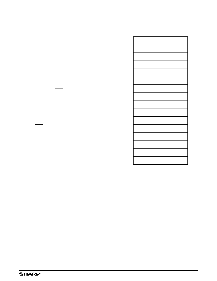
bytes) of 8 bits each. Sixteen 64K (65,536 Byte) blocks
are included on the LH28F008SA. A memory map is
shown in Figure 4 of this specification. A block erase
operation erases one of the sixteen blocks of memory
in typically 1.6 seconds, independent of the remaining
blocks. Each block can be independently erased and
written 100,000 cyles. Erase Suspend mode allows sys-
tem software to suspend block erase to read data or
execute code from any other block of the LH28F008SA.
The LH28F008SA is available in the 40-pin TSOP
(Thin Small Outline Package, 1.2 mm thick) package.
Pinouts are shown in Figure 1 of this specification.
The Command User Interface serves as the inter-
face between the microprocessor or microcontroller and
the internal operation of the LH28F008SA.
Byte Write and Block Erase Automation allow byte
write and block erase operations to be executed using
a two-write command sequence to the Command User
Interface. The internal Write State Machine (WSM)
automatically executes the algorithms and timings nec-
essary for byte write and block erase operations,
including verifications, thereby unburdening the micro-
processor or microcontroller. Writing of memory data is
performed in byte increments typically within 9 µs, an
80% improvement over current flash memory products.
I
PP
byte write and block erase currents are 10 mA typi-
cal, 30 mA maximum. V
PP
byte write and block erase
voltage is 11.4 V to 12.5 V.
The Status Register indicates the status of the WSM
and when the WSM successfully completes the desired
byte write or block erase operation.

8M (1M ◊ 8) Flash Memory
LH28F008SA
3
Figure 3. LH28F008SA Block Diagram
OUTPUT
BUFFER
IDENTIFIER
REGISTER
DATA
REGISTER
STATUS
REGISTER
INPUT
BUFFER
A
0
- A
19
DQ
0
- DQ
7
ADDRESS
LATCH
I/O LOGIC
DATA
COMPARATOR
WRITE STATE
MACHINE
RY/BY
PWD
OE
WE
CE
PROGRAM/
ERASE
VOLTAGE
SWITCH
Y-GATING
OUTPUT
MULTIPLEXER
Y-DECODER
X-DECODER
COMMAND
USER
INTERFACE
INPUT
BUFFER
. . .
ADDRESS
COUNTER
V
CC
V
PP
GND
16 64KB BLOCKS
28F008SA-2

LH28F008SA
8M (1M ◊ 8) Flash Memory
4
PIN DESCRIPTION
SYMBOL
TYPE
NAME AND FUNCTION
A
0
- A
19
INPUT
ADDRESS INPUTS:
For memory addresses. Addresses are internally latched during
a write cycle.
DQ
0
- DQ
7
INPUT/OUTPUT
DATA INPUT/OUTPUTS:
Inputs data and commands during Command User Interface
write cycles; outputs data during memory array. Status Register and Identifier read
cycles. The data pins are active high and float to tri-state off when the chip is deselected
or the outputs are disabled. Data is internally latched during a write cycle.
CE
ª
INPUT
CHIP ENABLE:
Activates the device's control logic input buffers, decoders, and
sense amplifiers. CE
ª
is active low: CE
ª
high deselects the memory device and
reduces power consumption to standby levels.
PWD
INPUT
POWERDOWN:
Puts the device in deep powerdown mode. PWD is active low; PWD
high gates normal operation. PWD also locks out block erase or byte write
operations when active low, providing data protection during power transitions.
OE
ª
INPUT
OUTPUT ENABLE:
Gates the device's outputs through the data buffers during a
read cycle. OE
ª
is active low.
WE
INPUT
WRITE ENABLE:
Controls writes to the Command User Interface and array blocks.
WE is active low. Addresses and data are latched on the rising edge of the
WE Pulse.
RY
ª
/BY
ª
OUTPUT
READY/BUSY
: Indicates the status of the internal Write State Machine. When low, it
indicates that the WSM is performing a block erase or byte write operation. RY
ª
/BY
ª
high indicates that the WSM is ready for new commands, block erase is suspended or
the device is in deep powerdown mode. RY
ª
/BY
ª
is always active and does NOT float
to tri-state off when the chip is deselected or data outputs are disabled.
V
PP
SUPPLY
BLOCK ERASE/BYTE WRITE POWER SUPPLY:
for erasing blocks of the array or
writing bytes of each block.
NOTE:
With V
PP
< V
PPLMAX
, memory contents cannot be altered.
V
CC
DEVICE POWER SUPPLY:
(5 V ±10%, 5 V ±5%)
GND
SUPPLY
GROUND
8M (1M ◊ 8) Flash Memory
LH28F008SA
5
Commands are written using standard microproces-
sor write timings. Command User Interface contents
serve as input to the WSM, which controls the block
erase and byte write circuitry. Write cycles also inter-
nally latch addresses and data needed for byte write or
block erase operations. With the appropriate command
written to the register, standard microprocessor read
timings output array data, access the intelligent identi-
fier codes, or output byte write and block erase status
for verification.
The RY
ª
/BY
ª
output gives an additional indicator of
WSM activity, providing capability for both hardware sig-
nal of status (versus software polling) and status mask-
ing (interrupt masking for background erase, for
example). Status polling using RY
ª
/BY
ª
minimizes both
CPU overhead and system power consumption. When
low, RY
ª
/BY
ª
indicates that the WSM is performing a block
erase or byte write operation. RY
ª
/BY
ª
high indicates that
the WSM is ready for new commands, block erase is
suspended or the device is in deep power down mode.
Maximum access time is 85 ns (t
ACC
) over the com-
mercial temperature range (0∞C to +70∞C) and over V
CC
supply voltage range (4.5 V to 5.5 V and 4.75 V to
5.25 V). I
CC
active current (CMOS Read) is 20 mA typi-
cal, 35 mA maximum at 8 MHz.
When the CE
ª
and PWD pins are at V
CC
, the I
CC
CMOS Standby mode is enabled.
A Deep Powerdown mode is enabled when the PWD
pin is at GND, minimizing power consumption and pro-
viding write protection. I
CC
current in deep power down
is 0.20 µA typical. Reset time of 400 ns is required from
PWD switching high until outputs are valid to read
attempts. Equivalently, the device has a wake time of
1 µs from PWD high until writes to the Command User
Interface are recognized by the LH28F008SA. With PWD
at GND, the WSM is reset and the Status Register is
cleared.
PRINCIPLES OF OPERATION
The LH28F008SA includes on-chip write automation
to manage write and erase functions. The Write State
Machine allows for 100% TTL-level control inputs; fixed
power supplies during block erasure and byte write; and
minimal processor overhead with SRAM like interface
timings.
After initial device powerup, or after return from deep
powerdown mode (see Bus Operations), the
LH28F008SA functions as a read-only memory. Manipu-
lation of external memory-control pins allow array read,
standby and output disable operations. Both Status
Register and intelligent identifiers can also be accessed
through the Command User Interface when V
PP
= V
PPL
.
This same subset of operations is also available when
high voltage is applied to the V
PP
pin. In addition, high
voltage on V
PP
enables successful block erasure and
byte writing of the device. All functions associated with
altering memory contents - byte write, block erase,
status and intelligent identifier - are accessed via the
Command User Interface and verified through the
Status Register.
Figure 4. Memory Map
MEMORY MAP
FFFFF
F0000
EFFFF
E0000
DFFFF
D0000
CFFFF
C0000
BFFFF
B0000
AFFFF
A0000
9FFFF
90000
8FFFF
80000
7FFFF
70000
6FFFF
60000
5FFFF
50000
4FFFF
40000
3FFFF
30000
2FFFF
20000
1FFFF
10000
0FFFF
00000
64KB BLOCK
64KB BLOCK
64KB BLOCK
64KB BLOCK
64KB BLOCK
64KB BLOCK
64KB BLOCK
64KB BLOCK
64KB BLOCK
64KB BLOCK
64KB BLOCK
64KB BLOCK
64KB BLOCK
64KB BLOCK
64KB BLOCK
64KB BLOCK
28F008SA-4