
- 1 -
In the absence of confirmation by device specification sheets, SHARP takes no responsibility for any defects that may occur in equipment using any SHARP devices shown in catalogs, data books,
etc. Contact SHARP in order to obtain the latest device specification sheets before using any SHARP device.
DESCRIPTION
The LH28F016SC-L/SCH-L flash memories with
SmartVoltage technology are high-density, low-cost,
nonvolatile, read/write storage solution for a wide
range of applications. Their symmetrically-blocked
architecture, flexible voltage and enhanced cycling
capability provide for highly flexible component
suitable for resident flash arrays, SIMMs and
memory cards. Their enhanced suspend
capabilities provide for an ideal solution for code +
data storage applications. For secure code storage
applications, such as networking, where code is
either directly executed out of flash or downloaded
to DRAM, the LH28F016SC-L/SCH-L offer three
levels of protection : absolute protection with Vpp at
GND, selective hardware block locking, or flexible
software block locking. These alternatives give
designers ultimate control of their code security
needs.
FEATURES
∑ SmartVoltage technology
≠ 2.7 V (Read-only), 3.3 V or 5 V V
CC
≠ 3.3 V, 5 V or 12 V V
PP
∑ High performance read access time
LH28F016SC-L95/SCH-L95
≠ 95 ns (5.0±0.25 V)/100 ns (5.0±0.5 V)/
120 ns (3.3±0.3 V)/150 ns (2.7 to 3.6 V)
LH28F016SC-L12/SCH-L12
≠ 120 ns (5.0±0.5 V)/150 ns (3.3±0.3 V)/
170 ns (2.7 to 3.6 V)
∑ Enhanced automated suspend options
≠ Byte write suspend to read
≠ Block erase suspend to byte write
≠ Block erase suspend to read
∑ Enhanced data protection features
≠ Absolute protection with V
PP
= GND
≠ Flexible block locking
≠ Block erase/byte write lockout during power
transitions
∑ SRAM-compatible write interface
∑ High-density symmetrically-blocked architecture
≠ Thirty-two 64 k-byte erasable blocks
∑ Enhanced cycling capability
≠ 100 000 block erase cycles
≠ 3.2 million block erase cycles/chip
∑ Low power management
≠ Deep power-down mode
≠ Automatic power saving mode decreases I
CC
in static mode
∑ Automated byte write and block erase
≠ Command user interface
≠ Status register
∑ ETOX
TM
V nonvolatile flash technology
∑ Packages
≠ 40-pin TSOP Type I (TSOP040-P-1020)
Normal bend/Reverse bend
≠ 44-pin SOP (SOP044-P-0600)
[LH28F016SC-L]
≠ 48-ball CSP (FBGA048-P-0810)
ETOX is a trademark of Intel Corporation.
LH28F016SC-L/SCH-L
16 M-bit (2 MB x 8) SmartVoltage
Flash Memories
LH28F016SC-L/SCH-L
COMPARISON TABLE
VERSIONS
OPERATING
DC CHARACTERISTICS
PACKAGE
TEMPERATURE
V
CC
deep power-down current (MAX.)
LH28F016SC-L
0 to +70∞C
10 µA
40-pin TSOP (I), 44-pin SOP,
48-ball CSP
LH28F016SCH-L
≠40 to +85∞C
20 µA
40-pin TSOP (I), 48-ball CSP

LH28F016SC-L/SCH-L
- 2 -
PIN CONNECTIONS
44-PIN SOP [LH28F016SC-L]
(SOP044-P-0600)
V
PP
RP#
A
11
A
10
A
9
A
8
A
7
A
6
A
5
A
4
NC
NC
A
3
A
2
A
1
A
0
DQ
0
DQ
1
DQ
2
DQ
3
GND
GND
1
2
3
4
5
6
7
8
9
10
11
12
13
14
15
16
17
18
19
20
21
22
44
43
42
41
40
39
38
37
36
35
34
33
32
31
30
29
28
27
26
25
24
23
V
CC
CE#
A
12
A
13
A
14
A
15
A
16
A
17
A
18
A
19
NC
NC
A
20
NC
WE#
OE#
RY/BY#
DQ
7
DQ
6
DQ
5
DQ
4
V
CC
40-PIN TSOP (Type I)
(TSOP040-P-1020)
A
19
A
18
A
17
A
16
A
15
A
14
A
13
A
12
CE#
V
CC
V
PP
RP#
A
11
A
10
A
9
A
8
A
7
A
6
A
5
A
4
1
2
3
4
5
6
7
8
9
10
11
12
13
14
15
16
17
18
19
20
40
39
38
37
36
35
34
33
32
31
30
29
28
27
26
25
24
23
22
21
A
20
NC
WE#
OE#
RY/BY#
DQ
7
DQ
6
DQ
5
DQ
4
V
CC
GND
GND
DQ
3
DQ
2
DQ
1
DQ
0
A
0
A
1
A
2
A
3
A
5
H
1
A
6
2
A
4
3
A
3
4
A
1
5
A
2
A
8
G
A
9
A
7
A
0
DQ
1
DQ
0
A
11
V
PP
V
CC
F
A
10
DQ
2
GND
DQ
3
E
NC
NC
NC
GND
D
NC
NC
NC
NC
V
CC
A
12
C
CE#
A
13
DQ
6
DQ
4
DQ
5
A
15
B
A
14
A
16
RY/BY#
DQ
7
NC
A
18
A
A
17
A
19
A
20
OE#
WE# 6
NC
RP#
(FBGA048-P-0810)
48-BALL CSP
A
1
TOP VIEW
NOTE :
Reverse bend available on request.

LH28F016SC-L/SCH-L
- 3 -
BLOCK DIAGRAM
Y GATING
Y DECODER
INPUT
BUFFER
OUTPUT
BUFFER
DQ
0
-DQ
7
V
CC
CE#
WE#
OE#
RP#
ADDRESS
LATCH
DATA
COMPARATOR
PROGRAM/ERASE
VOLTAGE SWITCH
STATUS
REGISTER
COMMAND
USER
INTERFACE
WRITE
STATE
MACHINE
DATA
REGISTER
OUTPUT
MULTIPLEXER
IDENTIFIER
REGISTER
ADDRESS
COUNTER
A
0
-A
20
X DECODER
32
64 k-BYTE
BLOCKS
RY/BY#
V
CC
GND
V
PP
INPUT
BUFFER
I/O
LOGIC

LH28F016SC-L/SCH-L
- 4 -
PIN DESCRIPTION
SYMBOL
TYPE
NAME AND FUNCTION
A
0
-A
20
INPUT
ADDRESS INPUTS : Inputs for addresses during read and write operations. Addresses
are internally latched during a write cycle.
INPUT/
DATA INPUT/OUTPUTS : Inputs data and commands during CUI write cycles; outputs
data during memory array, status register, and identifier code read cycles. Data pins
float to high-impedance when the chip is deselected or outputs are disabled. Data is
internally latched during a write cycle.
CE#
INPUT
CHIP ENABLE : Activates the device's control logic, input buffers, decoders, and sense
amplifiers. CE#-high deselects the device and reduces power consumption to standby
levels.
RESET/DEEP POWER-DOWN : Puts the device in deep power-down mode and resets
internal automation. RP#-high enables normal operation. When driven low, RP# inhibits
write operations which provide data protection during power transitions. Exit from deep
power-down sets the device to read array mode. RP# at V
HH
enables setting of the
master lock-bit and enables configuration of block lock-bits when the master lock-bit is
set. RP# = V
HH
overrides block lock-bits thereby enabling block erase and byte write
operations to locked memory blocks. Block erase, byte write, or lock-bit configuration
with V
IH
< RP# < V
HH
produce spurious results and should not be attempted.
OE#
INPUT
OUTPUT ENABLE : Gates the device's outputs during a read cycle.
WE#
INPUT
WRITE ENABLE : Controls writes to the CUI and array blocks. Addresses and data are
latched on the rising edge of the WE# pulse.
READY/BUSY : Indicates the status of the internal WSM. When low, the WSM is
performing an internal operation (block erase, byte write, or lock-bit configuration).
RY/BY#-high indicates that the WSM is ready for new commands, block erase is
suspended, and byte write is inactive, byte write is suspended, or the device is in deep
power-down mode. RY/BY# is always active and does not float when the chip is
deselected or data outputs are disabled.
BLOCK ERASE, BYTE WRITE, LOCK-BIT CONFIGURATION POWER SUPPLY : For
erasing array blocks, writing bytes, or configuring lock-bits. With V
PP
V
PPLK
, memory
contents cannot be altered. Block erase, byte write, and lock-bit configuration with an
invalid V
PP
(see Section 6.2.3 "DC CHARACTERISTICS") produce spurious results
and should not be attempted.
DEVICE POWER SUPPLY : Internal detection configures the device for 2.7 V , 3.3 V or
5 V operation. To switch from one voltage to another, ramp V
CC
down to GND and then
ramp V
CC
to the new voltage. Do not float any power pins. With V
CC
V
LKO
, all write
attempts to the flash memory are inhibited. Device operations at invalid V
CC
voltage
(see Section 6.2.3 "DC CHARACTERISTICS") produce spurious results and should
not be attempted. Block erase, byte write and lock-bit configuration operations with V
CC
<
3.0 V are not supported.
GND
SUPPLY
GROUND : Do not float any ground pins.
NC
NO CONNECT : Lead is not internal connected; recommend to be floated.
OUTPUT
DQ
0
-DQ
7
RP#
INPUT
RY/BY#
OUTPUT
V
PP
SUPPLY
V
CC
SUPPLY
LH28F016SC-L/SCH-L
1 INTRODUCTION
This datasheet contains LH28F016SC-L/SCH-L
specifications. Section 1 provides a flash memory
overview. Sections 2, 3, 4, and 5 describe the
memory organization and functionality. Section 6
covers electrical specifications. LH28F016SC-L/
SCH-L flash memories documentation also includes
ordering information which is referenced in
Section 7.
1.1
New Features
The LH28F016SC-L/SCH-L SmartVoltage flash
memories maintain backwards-compatibility with the
LH28F008SA. Key enhancements over the
LH28F008SA include :
∑ SmartVoltage Technology
∑ Enhanced Suspend Capabilities
∑ In-System Block Locking
Both devices share a compatible pinout, status
register, and software command set. These
similarities enable a clean upgrade from the
LH28F008SA to LH28F016SC-L/SCH-L. When
upgrading, it is important to note the following
differences :
∑ Because of new feature support, the two
devices have different device codes. This allows
for software optimization.
∑ V
PPLK
has been lowered from 6.5 V to 1.5 V to
support 3.3 V and 5 V block erase, byte write,
and lock-bit configuration operations. Designs
that switch V
PP
off during read operations
should make sure that the V
PP
voltage
transitions to GND.
∑ To take advantage of SmartVoltage technology,
allow V
PP
connection to 3.3 V or 5 V.
1.2 Product Overview
The LH28F016SC-L/SCH-L are high-performance
16 M-bit SmartVoltage flash memories organized
as 2 M-byte of 8 bits. The 2 M-byte of data is
arranged in thirty-two 64 k-byte blocks which are
individually erasable, lockable, and unlockable in-
system. The memory map is shown in Fig. 1.
SmartVoltage technology provides a choice of V
CC
and V
PP
combinations, as shown in Table 1, to
meet system performance and power expectations.
2.7 V V
CC
consumes approximately one-fifth the
power of 5 V V
CC
and 3.3 V V
CC
consumes
approximately one-fourth the power of 5 V V
CC
. But,
5 V V
CC
provides the highest read performance.
V
PP
at 3.3 V and 5 V eliminates the need for a
separate 12 V converter, while V
PP
= 12 V
maximizes block erase and byte write performance.
In addition to flexible erase and program voltages,
the dedicated V
PP
pin gives complete data
protection when V
PP
V
PPLK
.
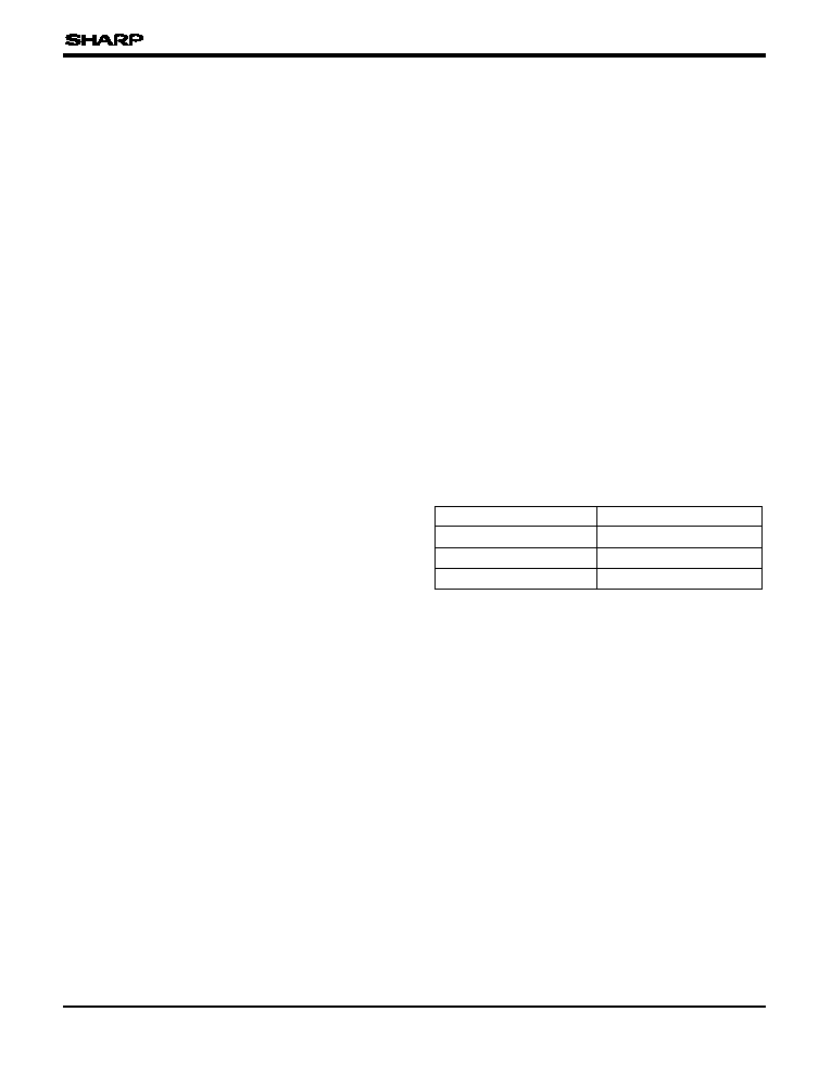
Table 1 V
CC
and V
PP
Voltage Combinations
Offered by SmartVoltage Technology
NOTE :
1.
Block erase, byte write and lock-bit configuration
operations with V
CC
< 3.0 V are not supported.
Internal V
CC
and V
PP
detection circuitry auto-
matically configures the device for optimized read
and write operations.
A Command User Interface (CUI) serves as the
interface between the system processor and
internal operation of the device. A valid command
sequence written to the CUI initiates device
automation. An internal Write State Machine (WSM)
automatically executes the algorithms and timings
necessary for block erase, byte write, and lock-bit
configuration operations.
A block erase operation erases one of the device's
64 k-byte blocks typically within 1 second (5 V V
CC
,
V
CC
VOLTAGE
V
PP
VOLTAGE
2.7 V
(NOTE 1)
--
3.3 V
3.3 V, 5 V, 12 V
5 V
5 V, 12 V
- 5 -