LH540203
CMOS 2048
◊
9 Asynchronous FIFO
FEATURES
∑∑
Fast Access Times: 15/20/25/35/50 ns
∑∑
Fast-Fall-Through Time Architecture Based on
CMOS Dual-Port SRAM Technology
∑∑
Input Port and Output Port Have Entirely
Independent Timing
∑∑
Expandable in Width and Depth
∑∑
Full, Half-Full, and Empty Status Flags
∑∑
Data Retransmission Capability
∑∑
TTL-Compatible I/O
∑∑
Pin and Functionally Compatible with Sharp LH5498
and with Am/IDT/MS7203
∑∑
Control Signals Assertive-LOW for Noise Immunity
∑∑
Packages:
28-Pin,
300-mil
PDIP
28-Pin,
300-mil
SOJ
*
32-Pin
PLCC
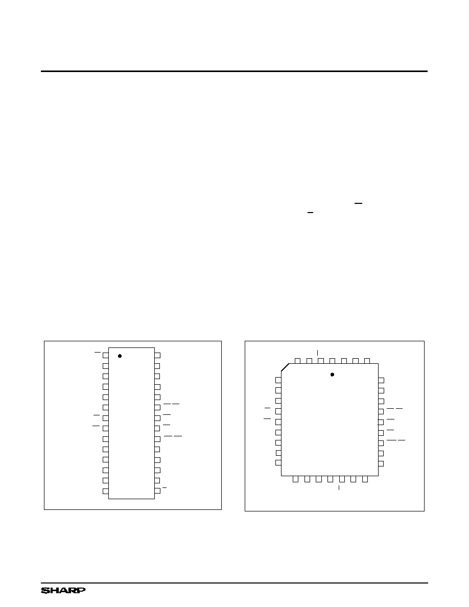
PIN CONNECTIONS
FUNCTIONAL DESCRIPTION
The LH540203 is a FIFO (First-In, First-Out) memory
device, based on fully-static CMOS dual-port SRAM tech-
nology, capable of storing up to 2048 nine-bit words. It
follows the industry-standard architecture and package
pinouts for nine-bit asynchronous FIFOs. Each nine-bit
LH540203 word may consist of a standard eight-bit byte,
together with a parity bit or a block-marking/framing bit.
The input and output ports operate entirely inde-
pendently of each other, unless the LH540203 becomes
either totally full or else totally empty. Data flow at a port
is initiated by asserting either of two asynchronous, as-
sertive-LOW control inputs: Write (W) for data entry at the
input port, or Read (R) for data retrieval at the output port.
Full, Half-Full, and Empty status flags monitor the
extent to which the internal memory has been filled. The
system may make use of these status outputs to avoid
the risk of data loss, which otherwise might occur either
by attempting to write additional words into an already-full
LH540203, or by attempting to read additional words from
an already-empty LH540203. When an LH540203 is
operating in a depth-cascaded configuration, the Half-Full
Flag is not available.
540203-2D
1
2
3
4
5
6
7
8
9
10
11
12
13
14
W
D
8
D
3
D
2
D
1
D
0
XI
FF
Q
0
Q
1
Q
2
Q
3
Q
8
V
SS
28
27
26
25
24
23
22
21
20
19
18
17
16
15
D
7
FL/RT
RS
EF
XO/HF
Q
5
Q
4
R
Q
6
Q
7
D
6
D
5
D
4
V
CC
28-PIN PDIP
28-PIN SOJ
*
TOP VIEW
Figure 1. Pin Connections for PDIP and
SOJ * Packages
5
6
7
8
9
10
D
2
XI
FF
11
2
3
4
32 31 30
29
28
27
26
25
24
NC
EF
D
3
D
8
W
NC
*
V
CC
D
4
D
5
14 15 16
20
19
18
17
FL/RT
RS
23
XO/HF
22
21
12
NC
13
1
Q
3
Q
8
V
SS
NC
*
R
Q
4
Q
5
540203-3D
D
1
D
0
Q
0
Q
1
Q
2
D
6
D
7
Q
7
Q
6
32-PIN PLCC
TOP VIEW
NOTE:
*
= No external electrical connections are allowed.
Figure 2. Pin Connections for PLCC Package
* This is a final data sheet; except that all references to the SOJ package have Advance Information status.
1

Data words are read out from the LH540203's output
port in precisely the same order that they were written in
at its input port; that is, according to a First-In, First Out
(FIFO) queue discipline. Since the addressing sequence
for a FIFO device's memory is internally predefined, no
external addressing information is required for the opera-
tion of the LH540203 device.
Drop-in-replacement compatibility is maintained with
both larger sizes and smaller sizes of industry-standard
nine-bit asynchronous FIFOs. The only change is in the
number of internally-stored data words implied by the
states of the Full Flag and the Half-Full Flag.
The Retransmit (RT) control signal causes the internal
FIFO-memory-array read-address pointer to be set back
to zero, to point to the LH540203's first physical memory
location, without affecting the internal FIFO-memory-
array write-address pointer. Thus, the Retransmit control
signal provides a mechanism whereby a block of data,
delimited by the zero physical address and the current
write-address-pointer value, may be read out
repeatedly
an arbitrary number of times. The only restrictions are that
neither the read-address pointer nor the write-address
pointer may `wrap around' during this entire process, i.e.,
advance past physical location zero after traversing the
entire memory. The retransmit facility is not available
when an LH540203 is operating in a depth-expanded
configuration.
The Reset (RS) control signal returns the LH540203
to an initial state, empty and ready to be filled. An
LH540203 should be reset during every system power-up
sequence. A reset operation causes the internal FIFO-
memory-array write-address pointer, as well as the read-
address pointer, to be set back to zero, to point to the
LH540203's first physical memory location. Any informa-
tion which previously had been stored within the
LH540203 is not recoverable after a reset operation.
A cascading (depth-expansion) scheme may be imple-
mented by using the Expansion In (XI) input signal and
the Expansion Out (XO/HF) output signal. This allows a
deeper `effective FIFO' to be implemented by using two
or more LH540203 devices, without incurring additional
latency (`fallthrough' or `bubblethrough') delays, and with-
out the necessity of storing and retrieving any given data
word more than once. In this cascaded operating mode,
one LH540203 device must be designated as the `first-
load' or `master' device, by grounding its First-Load
(FL/RT) control input; the remaining LH540203 devices
are designated as `slaves,' by tying their FL/RT inputs
HIGH. Because of the need to share control signals on
pins, the Half-Full Flag and the retransmission capability
are not available for either `master' or `slave' LH540203
devices operating in cascaded mode.
FUNCTIONAL DESCRIPTION (cont'd)
DATA OUTPUTS
Q
0
- Q
8
FLAG
LOGIC
WRITE
POINTER
READ
POINTER
DATA INPUTS
D
0
- D
8
DUAL-PORT
RAM
ARRAY
2048 x 9
EF
FF
. . .
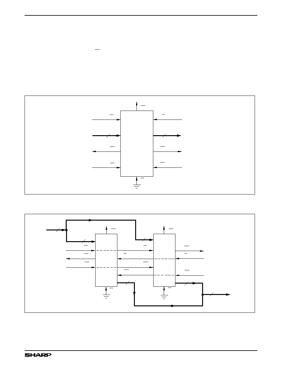
540203-1
INPUT
PORT
CONTROL
R
W
RESET
LOGIC
RS
OUTPUT
PORT
CONTROL
EXPANSION
LOGIC
XO/HF
XI
FL/RT
Figure 3. LH540203 Block Diagram
LH540203
CMOS 2048
◊
9 Asynchronous FIFO
2

OPERATIONAL DESCRIPTION
Reset
The LH540203 is reset whenever the Reset input (RS)
is taken LOW. A reset operation initializes both the read-
address pointer and the write-address pointer to point to
location zero, the first physical memory location. During
a reset operation, the state of the XI and FL/RT inputs
determines whether the device is in standalone mode or
in depth-cascaded mode. (See Tables 1 and 2.) The reset
operation forces the Empty Flag EF to be asserted
(EF = LOW), and the Half-Full Flag HF and the Full Flag
FF to be deasserted (HF = FF = HIGH); the Data Out pins
(D
0
≠ D
8
) are forced into a high-impedance state.
A reset operation is required whenever the LH540203
first is powered up. The Read (R) and Write (W) inputs
may be in any state when the reset operation is initiated;
but they must be HIGH, before the reset operation is
terminated by a rising edge of RS, by a time t
RRSS
(for
Read) or t
WRSS
(for Write) respectively. (See Figure 10.)
Write
A write cycle is initiated by a falling edge of the Write
(W) control input. Data setup times and hold times must
be observed for the data inputs (D
0
≠ D
8
). Write opera-
tions may occur independently of any ongoing read op-
erations. However, a write operation is possible only if the
FIFO is not full, (i.e., if the Full Flag FF is HIGH).
At the falling edge of W for the first write operation after
the memory is half filled, the Half-Full Flag is asserted
(HF = LOW). It remains asserted until the difference
between the write pointer and the read pointer indicates
that the data words remaining in the LH540203 are filling
the FIFO memory to less than or equal to one-half of its
total capacity. The Half-Full Flag is deasserted
(HF = HIGH) by the appropriate rising edge of R. (See
Table 3.)
The Full Flag is asserted (FF = LOW) at the falling edge
of W for the write operation which fills the last available
location in the FIFO memory array. FF = LOW inhibits
further write operations until FF is cleared by a valid read
operation. The Full Flag is deasserted (FF = HIGH) after
the next rising edge of R releases another memory loca-
tion. (See Table 3.)
Read
A read cycle is initiated by a falling edge of the Read
(R) control input. Read data becomes valid at the data
outputs (Q
0
≠ Q
8
) after a time t
A
from the falling edge of
R. After R goes HIGH, the data outputs return to a
high-impedance state. Read operations may occur inde-
pendently of any ongoing write operations. However, a
read operation is possible only if the FIFO is not empty
(i.e., if the Empty Flag EF is HIGH).
The LH540203's internal read-address and write-
address pointers operate in such a way that consecutive
read operations always access data words in the same
order that they were written. The Empty Flag is asserted
(EF = LOW) after that falling edge of R which accesses
the last available data word in the FIFO memory. EF is
deasserted (EF = HIGH) after the next rising edge of W
loads another valid data word. (See Table 3.)
Data Flow-Through
Read-data flow-through mode occurs when the Read
(R) control input is brought LOW while the FIFO is empty,
and is held LOW in anticipation of a write cycle. At the end
of the next write cycle, the Empty Flag EF momentarily is
deasserted, and the data word just written becomes
available at the data outputs (Q
0
≠ Q
8
) after a maxi-
mum time of t
WEF
+ t
A
. Additional write operations may occur
while the R input remains LOW; but only data from the
first write operation flows through to the data outputs.
Additional data words, if any, may be accessed only by
toggling R.
Write-data flow-through mode occurs when the Write
(W) input is brought LOW while the FIFO is full, and is
held LOW in anticipation of a read cycle. At the end of the
read cycle, the Full Flag momentarily is deasserted, but
then immediately is reasserted in response to W being
held LOW. A data word is written into the FIFO on the
rising edge of W, which may occur no sooner than
t
RFF
+ t
WPW
after the read operation.
PIN DESCRIPTIONS
PIN
PIN TYPE
1
DESCRIPTION
D
0
≠ D
8
I
Input Data Bus
Q
0
≠ Q
8
O/Z
Output Data Bus
W
I
Write Request
R
I
Read Request
EF
O
Empty Flag
FF
O
Full Flag
PIN
PIN TYPE
1
DESCRIPTION
XO/HF
O
Expansion Out/Half-Full Flag
XI
I
Expansion In
FL/RT
I
First Load/Retransmit
RS
I
Reset
V
CC
V
Positive Power Supply
V
SS
V
Ground
NOTE:
1.
I = Input, O = Output, Z = High-Impedance, V = Power Voltage Level
CMOS 2048
◊
9 Asynchronous FIFO
LH540203
3

OPERATIONAL DESCRIPTION (cont'd)
Retransmit
The FIFO can be made to reread previously-read data
by means of the Retransmit function. A retransmit opera-
tion is initiated by pulsing the RT input LOW. Both R and
W must be deasserted (HIGH) for the duration of the
retransmit pulse. The FIFO's internal read-address
pointer is reset to point to location zero, the first physical
memory location, while the internal write-address
pointer remains unchanged.
After a retransmit operation, those data words in the
region in between the read-address pointer and the
write-address pointer may be reaccessed by subsequent
read operations. A retransmit operation may affect the
state of the status flags FF, HF, and EF, depending on
the relocation of the read-address pointer. There is no
restriction on the number of times that a block of data
within an LH540203 may be read out, by repeating the
retransmit operation and the subsequent read operations.
The maximum length of a data block which may be
retransmitted is 2048 words. Note that if the write-address
pointer ever `wraps around' (i.e., passes location zero
more than once) during a sequence of retransmit opera-
tions, some data words will be lost.
The Retransmit function is not available when the
LH540203 is operating in depth-cascaded mode,
because the FL/RT control pin must be used for first-load
selection rather than for retransmission control.
Table 1. Grouping-Mode Determination
During a Reset Operation
XI
FL/
RT
MODE
XO/HF
USAGE
XI
USAGE
FL/RT
USAGE
H
1
H
Cascaded
Slave
2
XO
XI
FL
H
1
L
Cascaded
Master
2
XO
XI
FL
L
X
Standalone
HF
(none)
RT
NOTES:
1. A reset operation forces XO HIGH for the n
th
FIFO, thus forcing
XI HIGH for the (n+1)
st
FIFO.
2. The terms `master' and `slave' refer to operation in depth-cas-
caded grouping mode.
3. H = HIGH; L = LOW; X = Don't Care.
Table 2. Expansion-Pin Usage According to
Grouping Mode
I/O
PIN
STANDALONE
CASCADED
MASTER
CASCADED
SLAVE
I
XI
Grounded
From XO
(n-1st
FIFO)
From XO
(n-1st
FIFO)
O
XO/HF
Becomes
HF
To XI
(n+1st
FIFO)
To XI
(n+1st
FIFO)
I
FL/RT
Becomes
RT
Grounded
(Logic
LOW)
Logic
HIGH
Table 3. Status Flags
NUMBER OF UNREAD DATA
WORDS PRESENT WITHIN
2048
◊
9 FIFO
FF
HF
EF
0
H
H
L
1 to 1024
H
H
H
1025 to 2047
H
L
H
2048
L
L
H
LH540203
CMOS 2048
◊
9 Asynchronous FIFO
4
OPERATIONAL MODES
Standalone Configuration
When depth cascading is not required for a given
application, the LH540203 is placed in standalone mode
by tying the Expansion In input (XI) to ground. This
input is internally sampled during a reset operation. (See
Table 1.)
Width Expansion
Word-width expansion is implemented by placing mul-
tiple LH540203 devices in parallel. Each LH540203
should be configured for standalone mode. In this ar-
rangement, the behavior of the status flags is identical for
all devices; so, in principle, a representative value for
each of these flags could be derived from any one device.
In practice, it is better to derive `composite' flag values
using external logic, since there may be minor speed
variations between different actual devices. (See Figures
4, 5, and 6.)
WRITE
DATA IN
D
0
- D
8
9
FULL FLAG
RESET
XI
RT
RETRANSMIT
EMPTY FLAG
9
READ
HF
LH540203
W
FF
RS
R
EF
DATA OUT
Q
0
- Q
8
540203-17
Figure 4. Standalone FIFO (2048
◊
9)
18
WRITE
FULL FLAG
RESET
9
READ
EMPTY FLAG
R
EF
XI
RT
R
W
540203-18
RS
RETRANSMIT
RT
XI
HF
W
FF
RS
9
18
9
HF
9
LH540203
LH540203
DATA IN
D
0
- D
17
DATA OUT
Q
0
- Q
17
Figure 5. FIFO Word-Width Expansion (2048
◊
18)
CMOS 2048
◊
9 Asynchronous FIFO
LH540203
5
OPERATIONAL MODES (cont'd)
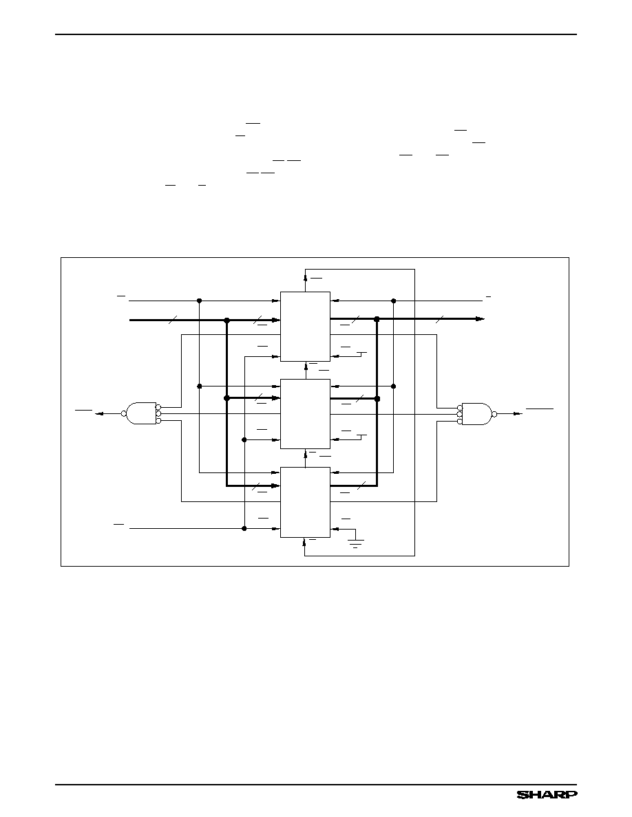
Depth Cascading
Depth cascading is implemented by configuring the
required number of LH540203s in depth-cascaded mode.
In this arrangement, the FIFOs are connected in a circular
fashion, with the Expansion Out output (XO) of each
device tied to the Expansion In input (XI) of the next
device. One FIFO in the cascade must be designated as
the `first-load' device, by tying its First Load input (FL/RT)
to ground. All other devices must have their FL/RT inputs
tied HIGH. In this mode, W and R signals are shared by
all devices, while logic within each LH540203 controls the
steering of data. Only one LH540203 is enabled during
any given write cycle; thus, the common Data In inputs of
all devices are tied together. Likewise, only one
LH540203 is enabled during any given read cycle; thus,
the common Data Out outputs of all devices are wire-
ORed together.
In depth-cascaded mode, external logic should be
used to generate a composite Full Flag and a composite
Empty Flag, by ANDing the FF outputs of all LH540203
devices together and ANDing the EF outputs of all devices
together. Since FF and EF are assertive-LOW signals,
this `ANDing' actually is implemented using an asser-
tive-HIGH physical OR gate. The Half-Full Flag and the
Retransmit function are not available in depth-cascaded
mode.
LH540203
RS
RS
FF
9
9
RS
W
FF
RS
FF
9
9
9
R
9
FL
FL
EF
XI
XO
FL
EF
Vcc
Vcc
XO
XO
9
9
XI
540203-19
XI
EMPTY
FULL
EF
LH540203
LH540203
DATA IN
D
0
- D
8
DATA OUT
Q
0
- Q
8
Figure 6. FIFO Depth Cascading (6144
◊
9)
LH540203
CMOS 2048
◊
9 Asynchronous FIFO
6

OPERATIONAL MODES (cont'd)
Compound FIFO Expansion
A combination of word-width expansion and depth
cascading may be implemented easily by operating
groups of depth-cascaded FIFOs in parallel.
Bidirectional FIFO Operation
Bidirectional data buffering between two systems may
be implemented by operating LH540203 devices in par-
allel, but in opposite directions. The Data In inputs of each
LH540203 are tied to the corresponding Data Out outputs
of another LH540203, which is operating in the opposite
direction, to form a single bidirectional bus interface. Care
must be taken to assure that the appropriate read, write,
and flag signals are routed to each system. Both word-
width expansion and depth cascading may be used in
bidirectional applications.
LH540203
DEPTH EXPANSION
BLOCK
LH540203
DEPTH EXPANSION
BLOCK
LH540203
DEPTH EXPANSION
BLOCK
Q
0
- Q
8
DATA OUT
D
N-9
-
D
N-1
D
18
- D
N-1
D
9
- D
N-1
D
0
- D
N-1
DATA IN
R
W
RS
Q
0
- Q
N-1
Q
0
- Q
17
540203-20
ARRAY STORES
N-BIT WORDS.
Q
0
- Q
N-10
Figure 7. Compound FIFO Expansion
LH540203
LH540203
SYSTEM A
SYSTEM B
Qb
0 - 8
Db
0 - 8
Da
0 - 8
Qa
0 - 8
XI
Wb
Ra
EFa
HFa
RTa
RS
FFb
RTb
HFb
EFb
Rb
540203-21
XI
Wa
FFa
RS
Figure 8. Bidirectional FIFO Operation
(2048
◊
9
◊
2)
CMOS 2048
◊
9 Asynchronous FIFO
LH540203
7

ABSOLUTE MAXIMUM RATINGS
1
PARAMETER
RATING
Supply Voltage to V
SS
Potential
≠0.5 V to 7 V
Signal Pin Voltage to V
SS
Potential
2
≠0.5 V to V
CC
+ 0.5 V (not to exceed 7 V)
DC Output Current
3
±
50 mA
Storage Temperature Range
≠65
o
C to 150
o
C
Power Dissipation (Package Limit)
1.0 W
DC Voltage Applied to Outputs In High-Z State
≠0.5 V to V
CC
+ 0.5 V (not to exceed 7 V)
NOTES:
1.
Stresses greater than those listed under `Absolute Maximum Ratings' may cause permanent damage to the device.
This is a stress rating for transient conditions only. Functional operation of the device at these or any other conditions
outside of those indicated in the `Operating Range' of this specification is not implied. Exposure to absolute maximum
rating conditions for extended periods may affect reliability.
2.
Negative undershoots of 1.5 V in amplitude are permitted for up to 10 ns once per cycle.
3.
Outputs should not be shorted for more than 30 seconds. No more than one output should be shorted at any time.
OPERATING RANGE
SYMBOL
PARAMETER
MIN
MAX
UNIT
T
A
Temperature, Ambient
0
70
∞
C
V
CC
Supply Voltage
4.5
5.5
V
V
SS
Supply Voltage
0
0
V
V
IL
Logic LOW Input Voltage
1
≠0 .5
0.8
V
V
IH
Logic HIGH Input Voltage
2.0
V
CC
+ 0.5
V
NOTE:
1.
Negative undershoots of 1.5 V in amplitude are permitted for up to 10 ns once per cycle.
DC ELECTRICAL CHARACTERISTICS (Over Operating Range)
SYMBOL
PARAMETER
TEST CONDITIONS
MIN
MAX
UNIT
I
LI
Input Leakage Current
V
CC
= 5.5 V, V
IN
= 0 V to V
CC
≠10
10
µ
A
I
LO
Output Leakage Current
R
V
IH
, 0 V
V
OUT
V
CC
≠10
10
µ
A
V
OH
Output HIGH Voltage
I
OH
= ≠2 .0 mA
2.4
V
V
OL
Output LOW Voltage
I
OL
= 8.0 mA
0.4
V
I
CC
Average Supply Current
1
Measured at f = 40 MHz
100
mA
I
CC2
Average Standby Current
1
All Inputs = V
IH
15
mA
I
CC3
Power Down Current
1
All Inputs = V
CC
≠ 0.2 V
5
mA
NOTE:
1.
I
CC
, I
CC2
, and I
CC3
are dependent upon actual output loading and cycle rates. Specified values are with outputs open.
LH540203
CMOS 2048
◊
9 Asynchronous FIFO
8

AC TEST CONDITIONS
PARAMETER
RATING
Input Pulse Levels
V
SS
to 3 V
Input Rise and Fall Times (10% to 90%)
5 ns
Input Timing Reference Levels
1.5 V
Output Reference Levels
1.5 V
Output Load, Timing Tests
Figure 9
CAPACITANCE
1,2
PARAMETER
RATING
C
IN
(Input Capacitance)
5 pF
C
OUT
(Output Capacitance)
7 pF
NOTES:
1.
Sample tested only.
2.
Capacitances are maximum values at 25
o
C, measured at 1.0 MHz,
with V
IN
= 0 V.
540203-4
DEVICE
UNDER
TEST
+5 V
30 pF
1.1 k
680
INCLUDES JIG AND SCOPE CAPACITANCES
*
*
Figure 9. Output Load Circuit
CMOS 2048
◊
9 Asynchronous FIFO
LH540203
9

AC ELECTRICAL CHARACTERISTICS
1
(Over Operating Range)
SYMBOL
PARAMETER
t
A
= 15 ns
t
A
= 20 ns
t
A
= 25 ns
t
A
= 35 ns
t
A
= 50 ns
UNIT
MIN
MAX
MIN
MAX
MIN
MAX
MIN MAX
MIN MAX
READ CYCLE TIMING
t
RC
Read Cycle Time
25
≠
30
≠
35
≠
45
≠
65
≠
ns
t
A
Access Time
≠
15
≠
20
≠
25
≠
35
≠
50
ns
t
RR
Read Recovery Time
10
≠
10
≠
10
≠
10
≠
15
≠
ns
t
RPW
Read Pulse Width
2
15
≠
20
≠
25
≠
35
≠
50
≠
ns
t
RLZ
Data Bus Active from Read LOW
3
5
≠
5
≠
5
≠
5
≠
5
≠
ns
t
WLZ
Data Bus Active from Write HIGH
3,4
10
≠
10
≠
10
≠
10
≠
10
≠
ns
t
DV
Data Valid from Read Pulse HIGH
5
≠
5
≠
5
≠
5
≠
5
≠
ns
t
RHZ
Data Bus High-Z from Read HIGH
3
≠
15
≠
15
≠
15
≠
15
≠
20
ns
WRITE CYCLE TIMING
t
WC
Write Cycle Time
25
≠
30
≠
35
≠
45
≠
65
≠
ns
t
WPW
Write Pulse Width
2
15
≠
20
≠
25
≠
35
≠
50
≠
ns
t
WR
Write Recovery Time
10
≠
10
≠
10
≠
10
≠
15
≠
ns
t
DS
Data Setup Time
12
≠
12
≠
12
≠
15
≠
20
≠
ns
t
DH
Data Hold Time
0
≠
0
≠
0
≠
0
≠
0
≠
ns
RESET TIMING
t
RSC
Reset Cycle Time
25
≠
30
≠
35
≠
45
≠
65
≠
ns
t
RS
Reset Pulse Width
2
15
≠
20
≠
25
≠
35
≠
50
≠
ns
t
RSR
Reset Recovery Time
10
≠
10
≠
10
≠
10
≠
15
≠
ns
t
RRSS
Read HIGH to RS HIGH
15
≠
20
≠
25
≠
35
≠
50
≠
ns
t
WRSS
Write HIGH to RS HIGH
15
≠
20
≠
25
≠
35
≠
50
≠
ns
RETRANSMIT TIMING
5
t
RTC
Retransmit Cycle Time
25
≠
30
≠
35
≠
45
≠
65
≠
ns
t
RT
Retransmit Pulse Width
2
15
≠
20
≠
25
≠
35
≠
50
≠
ns
t
RTR
Retransmit Recovery Time
10
≠
10
≠
10
≠
10
≠
15
≠
ns
FLAG TIMING
t
EFL
Reset LOW to Empty Flag LOW
≠
25
≠
30
≠
35
≠
45
≠
65
ns
t
HFH,FFH
Reset LOW to Half-Full and Full
Flags HIGH
≠
25
≠
30
≠
35
≠
45
≠
65
ns
t
REF
Read LOW to Empty Flag LOW
≠
15
≠
20
≠
25
≠
35
≠
45
ns
t
RFF
Read HIGH to Full Flag HIGH
≠
15
≠
20
≠
25
≠
35
≠
45
ns
t
WEF
Write HIGH to Empty Flag HIGH
≠
15
≠
20
≠
25
≠
35
≠
45
ns
t
WFF
Write LOW to Full Flag LOW
≠
15
≠
20
≠
25
≠
35
≠
45
ns
t
WHF
Write LOW to Half-Full Flag LOW
≠
15
≠
20
≠
25
≠
35
≠
45
ns
t
RHF
Read HIGH to Half-Full Flag HIGH
≠
15
≠
20
≠
25
≠
35
≠
45
ns
EXPANSION TIMING
t
XOL
Expansion Out LOW
≠
18
≠
20
≠
25
≠
35
≠
50
ns
t
XOH
Expansion Out HIGH
≠
18
≠
20
≠
25
≠
35
≠
50
ns
t
XI
Expansion In Pulse Width
15
≠
20
≠
25
≠
35
≠
50
≠
ns
t
XIR
Expansion In Recovery Time
10
≠
10
≠
10
≠
10
≠
10
≠
ns
t
XIS
Expansion in Setup Time
7
≠
10
≠
10
≠
15
≠
15
≠
ns
NOTES:
1. All timing measurements are performed at `AC Test Condition' levels.
2. Pulse widths less than minimum value are not allowed.
LH540203
CMOS 2048
◊
9 Asynchronous FIFO
10

TIMING DIAGRAMS
t
RS
EFL
t
RSR
t
RRSS
t
WRSS
t
FFH
t
HFH
t
,
RS
R,W
EF
FF,HF
540203-14
t
RSC
NOTES:
1. t
RSC
= t
RS
+ t
RSR
.
2. W and R
V
IH
around the rising edge of RS.
3. The Data Out pins (D
0
- D
8
) are forced into a
high-impedance state whenever EF = LOW.
Figure 10. Reset Timing
W
t
WPW
t
RLZ
t
A
t
WC
t
A
t
RPW
t
DV
t
RHZ
VALID DATA OUT
t
RR
R
t
RC
t
WR
t
DH
t
DS
VALID DATA IN
540203-5
Q
0
- Q
8
D
0
- D
8
VALID DATA OUT
VALID DATA IN
Figure 11. Asynchronous Write and Read Operation
CMOS 2048
◊
9 Asynchronous FIFO
LH540203
11

TIMING DIAGRAMS (cont'd)
FF
R
W
t
RFF
t
WFF
LAST WRITE
FIRST READ
540204-6
Figure 12. Full Flag From Last Write to First Read
EF
W
R
t
WEF
t
REF
LAST READ
FIRST WRITE
540203-7
NOTE: The Data Out pins (D
0
- D
8
) are forced into a
high-impedance state whenever EF = LOW.
Figure 13. Empty Flag From Last Read to First Write
LH540203
CMOS 2048
◊
9 Asynchronous FIFO
12

TIMING DIAGRAMS (cont'd)
VALID DATA IN
RPE
t
WEF
t
REF
t
WLZ
t
A
t
540203-8
W
R
EF
D
0
- D
8
Q
0
- Q
8
VALID DATA OUT
NOTES:
1. t
RPE
= t
RPW
2. t
RPE
: Effective Read Pulse Width after Empty Flag HIGH.
3. The Data Out pins (D
0
- D
8
) are forced into a
high-impedance state whenever EF = LOW.
Figure 14. Read Data Flow-Through
WPF
t
540203-9
R
W
FF
t
WFF
t
RFF
t
DH
t
DS
t
A
D
0
- D
8
Q
0
- Q
8
NOTES:
1. t
WPF
= t
WPW.
2. t
WPF
: Effective Write Pulse Width after Full Flag HIGH.
VALID DATA IN
VALID DATA OUT
Figure 15. Write Data Flow-Through
CMOS 2048
◊
9 Asynchronous FIFO
LH540203
13

TIMING DIAGRAMS (cont'd)
t
WEF
W
t
RPE
EF
R
540203-10
NOTES:
1. t
RPE
= t
RPW
2. t
RPE
: Effective Read Pulse Width after Empty Flag HIGH.
3. The Data Out pins (D
0
- D
8
) are forced into a
high-impedance state whenever EF = LOW.
Figure 16. Empty Flag Timing
R
FF
W
540203-11
NOTES:
1. t
WPF
= t
WPW.
2. t
WPF
: Effective Write Pulse Width after Full Flag HIGH.
t
RFF
t
WPF
Figure 17. Full Flag Timing
HF
W
R
t
RHF
t
WHF
540203-12
HALF-FULL
OR LESS
MORE THAN
HALF-FULL
HALF-FULL
OR LESS
Figure 18. Half-Full Flag Timing
LH540203
CMOS 2048
◊
9 Asynchronous FIFO
14

TIMING DIAGRAMS (cont'd)
RT
t
RTR
t
RT
R,W
540203-13
NOTES:
1. t
RTC
= t
RT
+ t
RTR
.
2. FF, HF, and EF may change state during retransmit; but they will
become valid by t
RTC
.
Figure 19. Retransmit Timing
t
XOL
t
XOH
READ FROM
LAST VALID
LOCATION
t
XOH
t
XOL
XO
540203-15
WRITE TO LAST
AVAILABLE
LOCATION
W
R
Figure 20. Expansion-Out Timing
t
XIS
R
540203-16
XI
W
WRITE TO FIRST
AVAILABLE
LOCATION
t
XIS
READ FROM FIRST
VALID
LOCATION
t
XIR
t
XI
Figure 21. Expansion-In Timing
CMOS 2048
◊
9 Asynchronous FIFO
LH540203
15

PACKAGE DIAGRAMS
28DIP-3
7.49 [0.295]
7.11 [0.280]
0.51 [0.020] MIN
4.57 [0.180]
MAX
3.43 [0.135]
3.18 [0.125]
2.54 [0.100]
TYP.
0.53 [0.021]
0.38 [0.015]
0.30 [0.012]
0.20 [0.008]
DETAIL
DIMENSIONS IN MM [INCHES]
34.80 [1.370]
34.54 [1.360]
0
∞
TO 15
∞
MAXIMUM LIMIT
MINIMUM LIMIT
3.30 [0.130]
7.62 [0.300]
TYP.
28DIP (DIP28-W-300)
28-pin, 300-mil PDIP
28SOJ300
DIMENSIONS IN MM [INCHES]
MAXIMUM LIMIT
MINIMUM LIMIT
28SOJ (SOJ28-P-300)
1.27 [0.050]
TYP.
0.53 [0.021]
0.33 [0.013]
DETAIL
7.9 [0.311]
7.5 [0.295]
8.63 [0.340]
8.23 [0.324]
18.7 [0.736]
18.3 [0.720]
1.15 [0.045]
0.85 [0.033]
0.64 [0.025] MIN
7.0 [0.276]
6.6 [0.260]
2.6 [0.102]
2.2 [0.087]
3.7 [0.146]
3.3 [0.130]
0.20 [0.008]
0.8 [0.031]
0.6 [0.024]
0.102 [0.004]
1
14
28
15
28-pin, 300-mil SOJ
LH540203
CMOS 2048
◊
9 Asynchronous FIFO
16

ORDERING INFORMATION
15
20
25
35
50
LH540203
Device Type
X
Package
- ##
Speed
540203MD
CMOS 2048 x 9 FIFO
Example: LH540203U-25 (CMOS 2048 x 9 FIFO, 32-pin PLCC, 25 ns)
Access Time (ns)
D 28-pin, 300-mil Plastic DIP (DIP28-W-300)
K 28-pin, 300-mil SOJ * (SOJ28-P-300)
U 32-pin Plastic Leaded Chip Carrier (PLCC32-P-R450)
* Contact a Sharp representative for availability of SOJ package.
1.27 [0.050]
4 SIDES BSC
14.05 [0.553]
13.89 [0.547]
15.11 [0.595]
14.86 [0.585]
11.51 [0.453]
11.35 [0.447]
12.57 [0.495]
12.32 [0.485]
3.56 [0.140]
3.12 [0.123]
2.41 [0.095]
1.52 [0.060]
0.81 [0.032]
0.66 [0.026]
0.53 [0.021]
0.33 [0.013]
32PLCC
MAXIMUM LIMIT
MINIMUM LIMIT
DIMENSIONS IN MM (INCHES)
0.38 [0.015]
MIN
DETAIL
10.92 [0.430]
9.91 [0.390]
13.46 [0.530]
12.45 [0.490]
0.10 [0.004]
32PLCC (PLCC32-P-R450)
32-pin, 450-mil PLCC
CMOS 2048
◊
9 Asynchronous FIFO
LH540203
17