 | –≠–ª–µ–∫—Ç—Ä–æ–Ω–Ω—ã–π –∫–æ–º–ø–æ–Ω–µ–Ω—Ç: LH543621 | –°–∫–∞—á–∞—Ç—å:  PDF PDF  ZIP ZIP |

LH543611/21
FEATURES
∑∑
Pin-Compatible and Functionally
Upwards-Compatible with Sharp LH5420 and
LH543601, but Deeper
∑∑
Expanded Control Register that is Fully
Readable as well as Writeable
∑∑
Fast Cycle Times: 18/20/25/30/35 ns
∑∑
Improved Input Setup and Flag Out Timing
∑∑
Two 512
◊
36-bit FIFO Buffers (LH543611) or
Two 1024
◊
36-bit FIFO Buffers (LH543621)
∑∑
Full 36-bit Word Width
∑∑
Selectable 36/18/9-bit Word Width on Port B;
Selection May be Changed Without Resetting
the BiFIFO
∑∑
Programmable Byte-Order Reversal ≠
`Big-Endian
Little-Endian Conversion'
∑∑
Independently-Synchronized (`Fully-Asynchronous')
Operation of Port A and Port B
∑∑
`Synchronous' Enable-Plus-Clock Control at
Both Ports
∑∑
R/W, Enable, Request, and Address Control Inputs
are Sampled on the Rising Clock Edge
∑∑
Synchronous Request/Acknowledge `Handshake'
Capability; Use is Optional
∑∑
Device Comes Up Into a Known Default State at
Reset; Programming is Allowed, but is not Required
∑∑
Asynchronous Output Enables
∑∑
Five Status Flags per Port: Full, Almost-Full,
Half-Full, Almost-Empty, and Empty
∑∑
All Flags are Independently Programmable for
Either Synchronous or Asynchronous Operation
∑∑
Almost-Full Flag and Almost-Empty Flag Have
Programmable Offsets
∑∑
Mailbox Registers with Synchronized Flags
∑∑
Data-Bypass Function
∑∑
Data-Retransmit Function
∑∑
Automatic Byte Parity Checking with
Programmable Parity Flag Latch
∑∑
Programmable Byte Parity Generation
∑∑
Programmable Byte, Half-Word, or Full-Word
Oriented Parity Operations
∑∑
8 mA-I
OL
High-Drive Three-State Outputs with
Built-In Series Resistor
∑∑
TTL/CMOS-Compatible I/O
∑∑
Space-Saving PQFP and TQFP Packages
FUNCTIONAL DESCRIPTION
The LH543611 and LH543621 contain two FIFO buff-
ers, FIFO #1 and FIFO #2. These operate in parallel, but
in opposite directions, for bidirectional data buffering.
FIFO #1 and FIFO #2 each are organized as 512 or 1024
by 36 bits. The LH543611 and LH543621 are ideal either
for wide unidirectional applications or for bidirectional
data applications; component count and board area are
reduced.
The LH543611 and LH543621 have two 36-bit ports,
Port A and Port B. Each port has its own port-synchro-
nous clock, but the two ports may operate asynchro-
nously relative to each other. Data flow is initiated at a port
by the rising edge of the appropriate clock; it is gated by
the corresponding edge-sampled enable, request, and
read/write control signals. At the maximum operating
frequency, the clock duty cycle may vary from 40% to
60%. At lower frequencies, the clock waveform may be
quite asymmetric, as long as the minimum pulse-width
conditions for clock-HIGH and clock-LOW remain satis-
fied; the LH543611 and LH543621 are fully-static parts.
Conceptually, the port clocks CK
A
and CK
B
are free-
running, periodic `clock' waveforms, used to control other
signals which are edge-sensitive. However, there actually
is not any absolute requirement that these `clock' wave-
forms must be periodic. An `asynchronous' mode of op-
e ration is p os sib le, in o ne o r bo th direc tio ns,
independently, if the appropriate enable and request in-
puts are continuously asserted, and enough aperiodic
`clock' pulses of suitable duration are generated by exter-
nal logic to cause all necessary actions to occur.
A synchronous request/acknowledge handshake
facility is provided at each port for FIFO data access. This
request/ acknowledge handshake resolves FIFO full and
empty boundary conditions, when the two ports are op-
erated asynchronously relative to each other.
FIFO status flags monitor the extent to which each
FIFO buffer has been filled. Full, Almost-Full, Half-Full,
Almost-Empty, and Empty flags are included for
each
FIFO. Each of these flags may be independently pro-
grammed for either synchronous or asynchronous opera-
tion. Also, the Almost-Full and Almost-Empty flags are
programmable over the entire FIFO depth, but are auto-
matically initialized to eight locations from the respective
FIFO boundaries at reset. A data block of 512 (LH543611)
or 1024 (LH543621) or fewer words may be retransmitted
any desired number of times.
512
◊
36
◊
2 / 1024
◊
36
◊
2
Synchronous Bidirectional FIFO
BOLD = Additions over the 5420/3601 feature set
1

Two mailbox registers provide a separate path for
passing control words or status words between ports.
Each mailbox has a New-Mail-Alert Flag, which is syn-
chronized to the reading port's clock. This mailbox func-
tion facilitates the synchronization of data transfers
between asynchronous systems.
Data-bypass mode allows Port A to directly transfer
data to or from Port B at reset. In this mode, the device
acts as a registered transceiver under the control of
Port A. For instance, a master processor on Port A can
use the data bypass feature to send or receive initializa-
tion or configuration information directly, to or from a
peripheral device on Port B, during system startup.
A word-width-select option is provided on Port B for
36-bit, 18-bit, or 9-bit data access. This feature allows
word-width matching between Port A and Port B, with no
additional logic needed. It also ensures maximum utiliza-
tion of bus band widths. Subject to meeting timing require-
ments, the word-width selection may be changed at any
time during the operation of an LH543611 or LH543621,
without the need either for a reset operation or for passing
dummy words through Port B immediately after the
change; except that if the change is not made at a
full-word boundary, at least one dummy word must be
passed through Port B before any actual data words
are transmitted.
A Byte Parity Check Flag at each port monitors data
integrity. Control-Register bit 00 (zero) selects the parity
mode, odd or even. This bit is initialized for odd data parity
at reset; but it may be reprogrammed for even parity, or
back again to odd parity, as desired. The parity flags may
be programmed to operate either in a latched mode or in
a flowthrough mode. The parity checking may be per-
formed over 36-bit full-words, over 18-bit half-words, or
over 9-bit single bytes.
Parity generation may be selected as well as parity
checking, and may likewise be performed over full-words
or half-words or single bytes. In any case, a parity bit of
the proper mode is generated over the least-significant
eight bits of a byte, and then is stored in the most-signifi-
cant bit position of the byte as it passes through the
LH543611/21, overwriting whatever bit was present in
that bit position previously.
LH543611/21
512 x 36 x 2/1024 x 36 x 2 BiFIFOs
2

116
115
114
113
112
111
110
109
108
107
106
105
104
103
102
101
100
99
98
97
96
95
94
93
92
91
90
89
88
87
86
85
84
18
19
20
21
22
23
24
25
26
27
28
29
30
31
32
33
34
35
36
37
38
39
40
41
42
43
44
45
46
47
48
V
CCO
D
10A
D
9A
D
8A
V
SSO
D
7A
D
6A
D
5A
D
4A
D
3A
D
2A
D
1A
D
0A
RS
RT
1
D
1B
D
2B
D
3B
D
4B
D
5B
D
6B
D
7B
D
8B
D
9B
D
10B
D
11B
V
CCO
V
SSO
V
SSO
V
CCO
V
SSO
V
CCO
49
50
D
0B
51
52
53
54
55
56
57
58
59
60
61
62
63
64
65
66
67
68
69
70
71
72
73
74
75
76
77
78
79
80
81
82
83
V
CCO
D
24A
D
25A
D
26A
V
SSO
D
27A
D
28A
D
29A
D
30A
D
31A
D
32A
D
33A
D
34A
D
35A
RT
2
D
35B
D
34B
D
33B
D
32B
D
31B
D
30B
D
29B
D
28B
D
27B
D
26B
D
25B
V
CCO
V
SSO
V
SS
V
SSO
V
CCO
V
SSO
V
CCO
17
16
15
14
13
12
11
10
9
8
7
6
5
4
3
2
Pin 1
Pin 132
131
130
129
128
127
126
125
124
123
122
121
120
119
118
117
D
12A
D
13A
D
14A
V
SSO
D
15A
D
16A
D
17A
HF
1
AF
1
FF
1
OE
A
A
2A
A
1A
A
0A
R/W
A
EN
A
V
SS
ACK
A
EF
2
MBF
2
D
18A
D
19A
D
20A
D
21A
D
22A
V
CC
CK
A
REQ
A
AE
2
V
SSO
D
23
A
D
11A
D
12B
D
13B
D
14B
V
SSO
D
15B
D
16B
D
17B
AE
1
EF
1
REQ
B
EN
B
R/W
B
CK
B
WS
0
WS
1
V
CC
FF
2
AF
2
PF
B
D
18B
D
19B
D
20B
D
21B
D
22B
V
SS
A
0B
HF
2
V
SSO
D
23
B
MBF
1
ACK
B
OE
B
D
24
B
PF
A
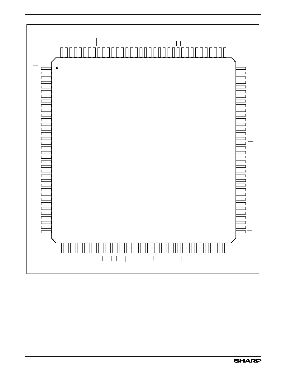
543611-1
TOP VIEW
CHAMFERED
EDGE
132-PIN PQFP
Figure 1. Pin Connections for 132-Pin PQFP Package
(Top View)
PIN CONNECTIONS
512 x 36 x 2/1024 x 36 x 2 BiFIFOs
LH543611/21
3
108
107
106
105
104
103
102
101
100
99
98
97
96
95
94
93
92
91
90
89
88
87
86
85
84
83
82
81
80
79
78
77
76
1
2
3
4
5
6
7
8
9
10
11
12
13
14
15
16
17
18
19
20
21
22
23
24
25
26
27
28
29
30
31
D
24A
D
25A
D
27A
D
28A
D
30A
D
31A
D
33A
D
34B
D
33B
D
31B
D
30B
D
28B
D
27B
32
33
RT
2
128
127
V
CCO
D
10A
D
9A
V
SSO
D
7A
D
6A
V
CCO
D
4A
D
3A
V
SSO
D
1A
RS
D
0B
D
2B
V
SSO
D
3B
D
5B
V
CCO
D
6B
D
8B
V
SSO
D
9B
D
5A
D
2A
D
1B
D
4B
D
7B
D
10B
144
143
142
141
140
139
138
137
136
135
134
133
132
131
130
129
126
125
124
123
122
121
120
119
118
117
116
115
114
113
112
D
23A
D
22A
D
21A
V
SSO
D
19A
D
18A
AE
2
EF
2
ACK
A
REQ
A
EN
A
R/W
A
CK
A
A
0A
OE
A
V
CC
FF
1
HF
1
PF
A
D
17A
D
15A
V
SSO
D
14A
V
SS
AF
1
D
13A
D
24B
D
23B
V
SSO
D
22B
D
20B
PF
B
OE
B
WS
1
A
0B
R/W
B
EN
B
REQ
B
ACK
B
EF
1
MBF
1
D
16B
V
SSO
V
SS
D
17B
D
15B
HF
2
CK
B
D
14B
TOP VIEW
MBF
2
543611-2
34
35
36
V
CCO
D
11B
V
CCO
75
74
73
111
110
D
12A
D
11A
109
53
54
37
38
39
40
41
42
43
44
45
46
47
48
49
50
51
52
55
56
57
58
59
60
61
62
63
64
65
66
67
68
69
70
71
72
D
13B
D
12B
V
CCO
D
26A
V
SSO
D
29A
V
CCO
D
32A
V
SSO
D
34A
D
35A
V
SSO
D
32B
V
CCO
D
29B
V
SSO
D
26B
D
25B
D
21B
D
19B
D
18B
AF
2
FF
2
V
CC
WS
0
AE
1
D
8A
RT
1
D
0A
D
20A
A
1A
A
2A
D
16A
D
35B
V
SS
144-PIN TQFP
V
SSO
V
SS
V
SSO
FR
1
V
SSO
V
CCO
V
CCO
V
SSO
V
SSO
V
SS
V
SSO
FR
2
Figure 2. Pin Connections for 144-Pin TQFP Package
(Top View)
LH543611/21
512 x 36 x 2/1024 x 36 x 2 BiFIFOs
4
PIN LIST
SIGNAL
NAME
PQFP
PIN NO.
TQFP
PIN NO.
A
0A
1
126
A
1A
2
125
A
2A
3
124
OE
A
4
123
FF
1
6
121
AF
1
7
120
HF
1
8
119
PF
A
9
118
D
17A
10
117
D
16A
11
116
D
15A
12
115
D
14A
14
113
D
13A
15
112
D
12A
16
111
D
11A
17
110
D
10A
19
106
D
9A
20
105
D
8A
21
104
D
7A
23
102
D
6A
24
101
D
5A
25
100
D
4A
27
98
D
3A
28
97
D
2A
29
96
D
1A
31
94
D
0A
32
93
RS
33
92
RT
1
34
91
D
0B
35
89
D
1B
36
88
D
2B
37
87
D
3B
39
85
D
4B
40
84
D
5B
41
83
D
6B
43
81
D
7B
44
80
D
8B
45
79
D
9B
47
77
D
10B
48
76
D
11B
49
75
D
12B
51
71
D
13B
52
70
D
14B
53
69
D
15B
54
68
D
16B
56
66
D
17B
57
65
MBF
1
58
64
AE
1
59
63
SIGNAL
NAME
PQFP
PIN NO.
TQFP
PIN NO.
EF
1
60
62
ACK
B
61
61
REQ
B
63
59
EN
B
64
58
R/W
B
65
57
CK
B
66
56
A
0B
67
55
WS
0
68
53
WS
1
69
52
OE
B
70
51
FF
2
72
49
AF
2
73
48
HF
2
74
47
PF
B
75
46
D
18B
76
45
D
19B
77
44
D
20B
78
43
D
21B
80
41
D
22B
81
40
D
23B
82
39
D
24B
83
38
D
25B
85
34
D
26B
86
33
D
27B
87
32
D
28B
89
30
D
29B
90
29
D
30B
91
28
D
31B
93
26
D
32B
94
25
D
33B
95
24
D
34B
97
22
D
35B
98
21
RT
2
100
18
D
35A
101
17
D
34A
102
16
D
33A
103
15
D
32A
105
13
D
31A
106
12
D
30A
107
11
D
29A
109
9
D
28A
110
8
D
27A
111
7
D
26A
113
5
D
25A
114
4
D
24A
115
3
D
23A
117
143
D
22A
118
142
D
21A
119
141
SIGNAL
NAME
PQFP
PIN122 NO.
TQFP
PIN NO.
D
20A
120
140
D
19A
122
138
D
18A
123
137
MBF
2
124
136
AE
2
125
135
EF
2
126
134
ACK
A
127
133
REQ
A
129
131
EN
A
130
130
R/W
A
131
129
CK
A
132
128
V
CC
5
122
V
SSO
13
114
V
SSO
109
V
CCO
108
V
CCO
18
107
V
SSO
22
103
V
CCO
26
99
V
SSO
30
95
V
SSO
90
V
SSO
38
86
V
CCO
42
82
V
SSO
46
78
V
CCO
50
74
V
CCO
73
V
SSO
72
V
SSO
55
67
V
SS
62
60
V
SS
54
V
CC
71
50
V
SSO
79
42
V
SSO
37
V
CCO
36
V
CCO
84
35
V
SSO
88
31
V
CCO
92
27
V
SSO
96
23
V
SS
99
20
V
SSO
19
V
SSO
104
14
V
CCO
108
10
V
SSO
112
6
V
CCO
116
2
V
CCO
1
V
SSO
144
V
SSO
121
139
V
SS
128
132
V
SS
127
NOTE:
PINS
COMMENTS
V
CC
Supply internal logic. Connected to each other.
V
CCO
Supply output drivers only. Connected to each
other.
PINS
COMMENTS
V
SS
Supply internal logic. Connected to each other.
V
SSO
Supply output drivers only. Connected to each
other.
512 x 36 x 2/1024 x 36 x 2 BiFIFOs
LH543611/21
5

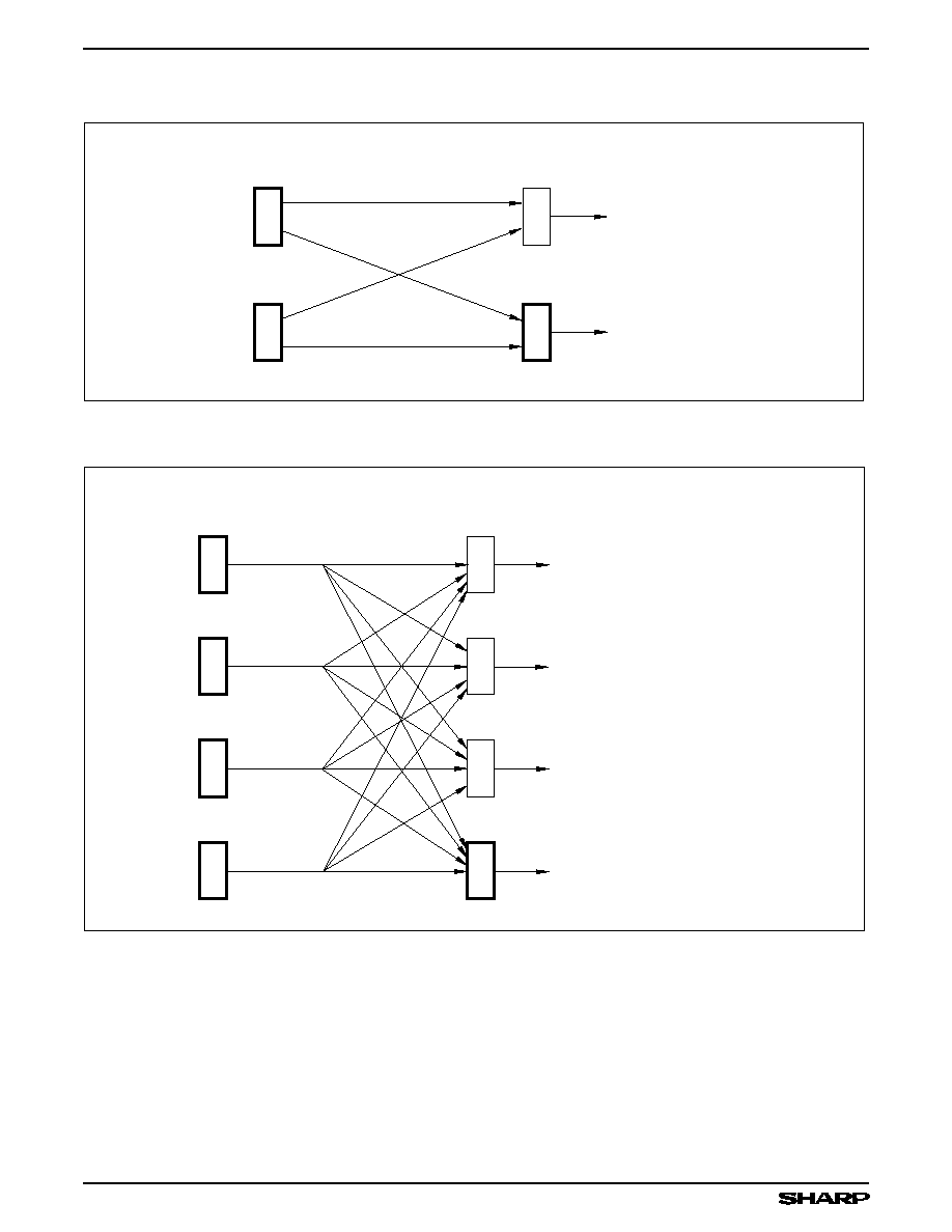
RESET
LOGIC
PORT A
I/O
RS
PORT A
SYNCH-
RONOUS
CONTROL
LOGIC
READ
POINTER
WRITE
POINTER
FIXED AND
PROGRAMMABLE
STATUS FLAGS
FIFO #1
MEMORY ARRAY
512 x 36 / 1024 x 36
MAILBOX
REGISTER
#2
READ
POINTER
WRITE
POINTER
FIFO #2
MEMORY ARRAY
512 x 36 / 1024 x 36
PORT B
I/O
FF
1
HF
1
AF
1
EF
2
AE
2
EF
1
AE
1
FF
2
HF
2
AF
2
WS
0
, WS
1
D
0A
- D
35A
OE
A
ACK
A
REQ
A
EN
A
R/W
A
CK
A
D
0B
- D
35B
OE
B
RT
1
ACK
B
REQ
B
EN
B
R/W
B
CK
B
COMMAND
PORT AND
REGISTER
A
0B
RESOURCE
REGISTERS
PARITY
CHECKING
AND
GENERATION
A
0A
A
1A
A
2A
RT
2
COMMAND
PORT AND
REGISTER
MAILBOX
REGISTER
#1
BYPASS
MBF
1
MBF
2
PORT B
SYNCH-
RONOUS
CONTROL
LOGIC
FIXED AND
PROGRAMMABLE
STATUS FLAGS
543611-4
PF
A
PF
B
PARITY
CHECKING
AND
GENERATION
FR
1
FR
2
Figure 3b. Detailed LH543611/21 Block Diagram
FIFO 1
PORT A
I/O
FIFO 2
PORT B
I/O
WRITE
READ
WRITE
READ
PORT A
CONTROL
PORT B
CONTROL
543611-3
Figure 3a. Simplified LH543611/21 Block Diagram
LH543611/21
512 x 36 x 2/1024 x 36 x 2 BiFIFOs
6

PIN DESCRIPTIONS
PIN
PIN TYPE
1
DESCRIPTION
GENERAL
V
CC
, V
SS
V
Power, Ground
RS
I
Reset
PORT A
CK
A
I
Port A Free-Running Clock
R/W
A
I
Port A Edge-Sampled Read/Write Control
EN
A
I
Port A Edge-Sampled Enable
A
0A
, A
1A
, A
2A
I
Port A Edge-Sampled Address Pins
OE
A
I
Port A Level-Sensitive Output Enable
REQ
A
I
Port A Request/Enable
RT
2
I
FIFO #2 Retransmit
D
0A
≠ D
35A
I/O/Z
Port A Bidirectional Data Bus
FF
1
O
FIFO #1 Full Flag (Write Boundary)
AF
1
O
FIFO #1 Programmable Almost-Full Flag (Write Boundary)
HF
1
O
FIFO #1 Half-Full Flag
AE
2
O
FIFO #2 Programmable Almost-Empty Flag (Read Boundary)
EF
2
O
FIFO #2 Empty Flag (Read Boundary)
MBF
2
O
New-Mail-Alert Flag for Mailbox #2
PF
A
O
Port A Parity Flag
ACK
A
O
Port A Acknowledge
PORT B
CK
B
I
Port B Free-Running Clock
R/W
B
I
Port B Edge-Sampled Read/Write Control
EN
B
I
Port B Edge-Sampled Enable
A
0B
I
Port B Edge-Sampled Address Pin
OE
B
I
Port B Level-Sensitive Output Enable
WS
0
, WS
1
I
Port B Word-Width Select
REQ
B
I
Port B Request/Enable
RT
1
I
FIFO #1 Retransmit
D
0B
≠ D
35B
I/O/Z
Port B Bidirectional Data Bus
FF
2
O
FIFO #2 Full Flag (Write Boundary)
AF
2
O
FIFO #2 Programmable Almost-Full Flag (Write Boundary)
HF
2
O
FIFO #2 Half-Full Flag
AE
1
O
FIFO #1 Programmable Almost-Empty Flag (Read Boundary)
EF
1
O
FIFO #1 Empty Flag (Read Boundary)
MBF
1
O
New-Mail-Alert Flag for Mailbox #1
PF
B
O
Port B Parity Flag
ACK
B
O
Port B Acknowledge
NOTE:
1.
I = Input, O = Output, Z = High-Impedance, V = Power Voltage Level
512 x 36 x 2/1024 x 36 x 2 BiFIFOs
LH543611/21
7

ABSOLUTE MAXIMUM RATINGS
1
PARAMETER
RATING
Supply Voltage to V
SS
Potential
≠ 0.5 V to 7 V
Signal Pin Voltage to V
SS
Potential
3
≠ 0.5 V to V
CC
+ 0.5 V
DC Output Current
2
±
40 mA
Storage Temperature Range
≠ 65
o
C to 150
o
C
Power Dissipation (Package Limit)
2 Watts (Quad Flat Pack)
NOTES:
1.
Stresses greater than those listed under `Absolute Maximum Ratings' may cause permanent damage to the device. This is a stress rating for
transient conditions only. Functional operation of the device at these or any other conditions outside those indicated in the `Operating Range'
of this specification is not implied. Exposure to absolute maximum rating conditions for extended periods may affect reliability.
2.
Outputs should not be shorted for more than 30 seconds. No more than one output should be shorted at any time.
3.
Negative undershoot of 1.5 V in amplitude is permitted for up to 10 ns, once per cycle.
OPERATING RANGE
SYMBOL
PARAMETER
MIN
MAX
UNIT
T
A
Temperature, Ambient
0
70
o
C
Vcc
Supply Voltage
4.5
5.5
V
Vss
Supply Voltage
0
0
V
V
IL
Logic LOW
Input Voltage
1
≠ 0.5
0.8
V
V
IH
Logic HIGH
Input Voltage
2.2
Vcc + 0.5
V
NOTE:
1.
Negative undershoot of 1.5 V in amplitude is permitted
for up to 10 ns, once per cycle.
DC ELECTRICAL CHARACTERISTICS (OVER OPERATING RANGE)
SYMBOL
PARAMETER
TEST CONDITIONS
MIN
TYP
MAX
UNIT
I
LI
Input Leakage Current
V
CC
= 5.5 V, V
IN
= 0 V To V
CC
≠10
≠
10
µ
A
I
LO
I/O Leakage Current
OE
V
IH
, 0 V
V
OUT
V
CC
≠10
≠
10
µ
A
V
OL
Logic LOW Output Voltage
I
OL
= 8.0 mA
≠
≠
0.4
V
V
OH
Logic HIGH Output Voltage
I
OH
= ≠8 .0 mA
2.4
≠
≠
V
I
CC
Average Supply Current
1, 2
Measured at f
CC
= MAX
≠
180
280
mA
I
CC2
Average Standby Supply
Current
1, 3
All Inputs = V
IHMIN
(Clocks idle)
≠
13
25
mA
I
CC3
Power-Down Supply
Current
1
All Inputs = V
CC
≠ 0.2 V (Clocks idle)
≠
0.002
1
mA
I
CC4
Power-Down Supply
Current
1, 3
All Inputs = V
CC
≠ 0.2 V
(Clocks running at f
CC
= MAX)
≠
10
25
mA
NOTES:
1.
I
CC
, I
CC2
, I
CC3
, and I
CC4
are dependent upon actual output loading, and I
CC
, I
CC4
are also dependent on cycle rates. Specified values are with
outputs open (for I
CC
: C
L
= 0 pF); and, for I
CC
and I
CC4
, operating at minimum cycle times.
2.
I
CC
(MAX.) using V
CC
= MAX = 5.5 V and `worst case' data pattern. I
CC
(TYP.) using V
CC
= 5 V and `average' data pattern.
3.
I
CC2
(TYP.) and I
CC4
(TYP.) using V
CC
= 5 V and T
A
= 25∞C.
LH543611/21
512 x 36 x 2/1024 x 36 x 2 BiFIFOs
8

AC TEST CONDITIONS
PARAMETER
RATING
Input Pulse Levels
V
SS
to 3 V
Input Rise and Fall Times
(10% to 90%)
5 ns
Output Reference Levels
1.5 V
Input Timing Reference Levels
1.5 V
Output Load, Timing Tests
Figure 5
CAPACITANCE
1,2
PARAMETER
RATING
C
IN
(Input Capacitance)
8 pF
C
OUT
(Output Capacitance)
8 pF
NOTES:
1.
Sample tested only.
2.
Capacitances are maximum values at 25
o
C, measured at 1.0 MHz, with V
IN
= 0 V.
543611-14
+5 V
470
240
DEVICE
UNDER
TEST
30 pF
NOTE:
*
= Includes jig and scope capacitances
*
Figure 4. Output Load Circuit
512 x 36 x 2/1024 x 36 x 2 BiFIFOs
LH543611/21
9

AC ELECTRICAL CHARACTERISTICS
1
(V
CC
= 5 V
±
+10%, T
A
= 0
∞
C to 70
∞
C)
SYMBOL
DESCRIPTION
≠18
≠20
≠25
≠30
≠35
UNITS
MIN
MAX
MIN
MAX
MIN
MAX
MIN
MAX
MIN
MAX
f
CC
Clock Cycle Frequency
--
55
--
50
--
40
--
33
--
28.5
MHz
t
CC
Clock Cycle Time
18
--
20
--
25
--
30
--
35
--
ns
t
CH
Clock HIGH Time
7
--
8
--
10
--
12
--
15
--
ns
t
CL
Clock LOW Time
7
--
8
--
10
--
12
--
15
--
ns
t
DS
Data Setup Time
7.5
--
7.5
--
9
--
10
--
12
--
ns
t
DH
Data Hold Time
0.5
--
0.5
--
0.5
--
0.5
--
0.5
--
ns
t
ES
Enable Setup Time
5.5
--
5.5
--
7.5
--
8.5
--
10.5
--
ns
t
EH
Enable Hold Time
0.5
--
0.5
--
0.5
--
0.5
--
0.5
--
ns
t
RWS
Read/Write Setup Time
5.5
--
5.5
--
7.5
--
8.5
--
10.5
--
ns
t
RWH
Read/Write Hold Time
0.5
--
0.5
--
0.5
--
0.5
--
0.5
--
ns
t
RQS
Request Setup Time
5.5
--
5.5
--
7.5
--
8.5
--
10.5
--
ns
t
RQH
Request Hold Time
0.5
--
0.5
--
0.5
--
0.5
--
0.5
--
ns
t
AS
Address Setup Time
2
7.5
--
7.5
--
9
--
10
--
12
--
ns
t
AH
Address Hold Time
2
0.5
--
0.5
--
0.5
--
0.5
--
0.5
--
ns
t
WSS
Width Select Setup Time
5.5
--
5.5
--
7.5
--
8.5
--
10.5
--
ns
t
WSH
Width Select Hold Time
3
0.5
--
0.5
--
0.5
--
0.5
--
0.5
--
ns
t
A
Data Output Access Time
--
13
--
13.8
--
16
--
20
--
25
ns
t
ACK
Acknowledge Access Time
--
9.5
--
9.5
--
13
--
16
--
18
ns
t
OH
Output Hold Time
4
--
4
--
4
--
4
--
4
--
ns
t
ZX
Output Enable Time, OE LOW to
D
0
≠ D
35
Low-Z
3
1.5
--
1.5
--
2
--
3
--
3
--
ns
t
XZ
Output Disable Time, OE HIGH
to D
0
≠ D
35
High-Z
3
--
9
--
9
--
12
--
15
--
20
ns
t
EF
Clock to EF Flag Valid
--
14
--
14.5
--
19
--
22
--
27
ns
t
FF
Clock to FF Flag Valid
--
14
--
14.5
--
19
--
22
--
27
ns
t
HF
Clock to HF Flag Valid
--
14
--
14.5
--
19
--
22
--
27
ns
t
AE
Clock to AE Flag Valid
--
14.5
--
15
--
19
--
22
--
27
ns
t
AF
Clock to AF Flag Valid
--
14.5
--
15
--
19
--
22
--
27
ns
t
MBF
Clock to MBF Flag Valid
--
10
--
10
--
13
--
18
--
23
ns
t
PF
Data to Parity Flag Valid
4
--
14
--
14
--
17
--
20
--
25
ns
t
RS
Reset/Retransmit Pulse Width
5
18
--
20
--
25
--
30
--
35
--
ns
t
RSS
Reset/Retransmit Setup Time
6
15
--
16
--
20
--
25
--
30
--
ns
t
RSH
Reset/Retransmit Hold Time
6
7.2
--
8
--
10
--
15
--
20
--
ns
t
RF
Reset LOW to Flag Valid
--
21
--
21
--
25
--
30
--
35
ns
t
FRL
First Read Latency
7
18
--
20
--
25
--
30
--
35
--
ns
t
FWL
First Write Latency
8
18
--
20
--
25
--
30
--
35
--
ns
t
BS
Bypass Data Setup
8.5
--
8.5
--
10
--
13
--
15
--
ns
t
BH
Bypass Data Hold
2
--
2
--
3
--
4
--
5
--
ns
t
BA
Bypass Data Access
--
15.5
--
16
--
18
--
23
--
28
ns
t
SKEW1
Skew Time Read-to-Write Clock
14
--
14.5
≠
19
--
22
--
27
--
ns
t
SKEW2
Skew Time Write-to-Read Clock
14
--
14.5
--
19
--
22
--
27
--
ns
NOTES:
1.
Timing measurements performed at `AC Test Condition' levels.
2.
t
AS
, t
AH
address setup times and hold times need only be satisfied at clock edges which occur while the corresponding enables are being as-
serted.
3.
Values are guaranteed by design; not currently production tested.
4.
Measured with Parity Flag operating in flowthrough mode.
5.
When CK
A
or CK
B
is enabled; t
RS
= t
RSS
+ t
CH
+ t
RSH
.
6.
t
RSS
and/or t
RSH
need not be met unless a rising edge of CK
A
occurs while EN
A
is being asserted, or else a rising edge of CK
B
occurs while
EN
B
is being asserted.
7.
t
FRL
is the minimum first-write-to-first-read delay, following an empty condition, which is required to assure valid read data.
8.
t
FWL
is the minimum first-read-to-first-write delay, following a full condition, which is required to assure successful writing of data.
LH543611/21
512 x 36 x 2/1024 x 36 x 2 BiFIFOs
10

OPERATIONAL DESCRIPTION
Reset
The device is reset whenever the asynchronous Reset
(RS) input is taken LOW, and at least one rising edge and
one falling edge of both CK
A
and CK
B
occur while RS is
LOW. A reset operation is required after power-up, before
the first write operation may occur. The LH543611/21 is
fully ready for operation after being reset. No device
programming is required if the default states described
below are acceptable.
A reset operation initializes the read-address and
write-address pointers for FIFO #1 and FIFO #2 to those
FIFO's first physical memory locations. If the respective
outputs are enabled, the initial contents of these first
locations appear at the outputs. FIFO and mailbox status
flags are updated to indicate an empty condition. In
addition, the programmable-status-flag offset values are
initialized to eight. Thus, the AE
1
/AE
2
flags get asserted
within eight locations of an empty condition, and the
AF
1
/AF
2
flags likewise get asserted within eight locations
of a full condition, for FIFO #1/FIFO #2 respectively.
Bypass Operation
During reset (whenever RS is LOW) the device acts
as a registered transceiver, bypassing the internal FIFO
memories. Port A acts as the master port. A write or read
operation on Port A during reset transfers data directly to
or from Port B. Port B is considered to be the slave, and
cannot perform write or read operations independently on
its own during reset.
The direction of the bypass data transmission is deter-
mined by the R/W
A
control input, which does not get
overridden by the RS input. Here, a `write' operation
means passing data from Port A to Port B, and a `read'
operation means passing data from Port B to Port A.
The bypass capability may be used to pass initializa-
tion or configuration data directly between a master proc-
essor and a peripheral device during reset.
Address Modes
Address pins select the device resource to be
accessed by each port. Port A has three resource-regis-
ter-select inputs, A
0A
, A
1A,
and A
2A
, which select between
FIFO access, mailbox-register access, control-register
access, and programmable flag-offset-value-register ac-
cess. Port B has a single address input, A
0B
, to select
between FIFO access or mailbox-register access.
The status of the resource-register-select inputs is
sampled at the rising edge of an enabled clock (CK
A
or
CK
B
). Resource-register select-input address definitions
are summarized in Table 1.
Table 1. Resource-Register Addresses
A
2A
A
1A
A
0A
RESOURCE
PORT A
H
H
H
FIFO
H
H
L
Mailbox
H
L
H
AF
2
, AE
2
, AF
1
, AE
1
Flag Offsets
Register (36-Bit Mode)
H
L
L
Control Register Flag-
Synchronization and Parity
Operating Mode
L
H
H
AE
1
Flag Offset Register
L
H
L
AF
1
Flag Offset Register
L
L
H
AE
2
Flag Offset Register
L
L
L
AF
2
Flag Offset Register
A
0B
RESOURCE
PORT B
H
FIFO
L
Mailbox
Control Register
The eighteen Control-Register bits govern the syn-
chronization mode of the fullness-status flags at each
port, the choice of odd or even parity at both ports, the
enabling of parity generation for data flow at each port,
the optional latching behavior of the parity-error flags at
each port, and the selection of a full-word or half-word or
single-byte field for parity checking. A reset operation
initi alizes the LH543611/21 Control Register for
LH5420/LH543601-compatible operation, but it may be
reprogrammed at will at any time during LH543611/21
operation.
FIFO Write
Port A writes to FIFO #1, and Port B writes to FIFO #2.
A write operation is initiated on the rising edge of a clock
(CK
A
or CK
B
) whenever: the appropriate enable (EN
A
or
EN
B
) is held HIGH; the appropriate request (REQ
A
or
REQ
B
) is held HIGH; the appropriate Read/Write control
(R/W
A
or R/W
B
) is held LOW; the FIFO address is
selected for the address inputs (A
2A
≠ A
0A
or A
0B
); and
the prescribed setup times and hold times are observed
for all of these signals. Setup times and hold times must
also be observed on the data-bus pins (D
0A
≠ D
35A
or
D
0B
≠ D
35B
).
Normally, the appropriate Output Enable signal (OE
A
or OE
B
) is HIGH, to disable the outputs at that port, so
that the data word present on the bus from external
sources gets stored. However, a `loopback' mode of
operation also is possible, in which the data word supplied
by the outputs of one internal FIFO is `turned around' at
the port and read back into the other FIFO. In this mode,
the outputs at the port are not disabled. To remain within
specification for all timing parameters, the Clock Cycle
Frequency must be reduced slightly below the value
512 x 36 x 2/1024 x 36 x 2 BiFIFOs
LH543611/21
11

which otherwise would be permissible for that speed
grade of LH543611/21.
When a FIFO full condition is reached, write operations
are locked out. Following the first read operation from a
full FIFO, another memory location is freed up, and the
corresponding Full Flag is deasserted (FF = HIGH). The
first write operation should begin no earlier than a First
Write Latency (t
FWL
) after the first read operation from a
full FIFO, to ensure that correct read data are retrieved.
(See Figures 33 and 34.)
FIFO Read
Port A reads from FIFO #2, and Port B reads from FIFO
#1. A read operation is initiated on the rising edge of a
clock (CK
A
or CK
B
) whenever: the appropriate enable
(EN
A
or EN
B
) is held HIGH; the appropriate request
(REQ
A
o r R EQ
B
) is held HIGH; the appropri ate
Read/Write control (R/W
A
o r R/W
B
) is held HIGH;
the FIFO address is selected for the address inputs
(A
2A
≠ A
0A
or A
0B
); and the prescribed setup times and
hold times are observed for all of these signals. Read data
becomes valid on the data-bus pins (D
0A
≠ D
35A
or
D
0B
≠ D
35B
) by a time t
A
after the rising clock (CK
A
or
CK
B
) edge, provided that the data outputs are enabled.
OE
A
and OE
B
are assertive-LOW, asynchronous, Out-
put Enable control input signals. Their effect is only to
enable or disable the output drivers of the respective port.
Disabling the outputs does
not disable a read operation;
data transmitted to the corresponding output register will
remain available later, when the outputs again are en-
abled, unless it subsequently is overwritten.
When an empty condition is reached, read operations
are locked out until a valid write operation(s) has loaded
additional data into the FIFO. Following the first write to
an empty FIFO, the corresponding empty flag (EF) will be
deasserted (HIGH). The first read operation should begin
no earlier than a First Read Latency (t
FRL
) after the first
write to an empty FIFO, to ensure that correct read data
words are retrieved. (See Figures 31 and 32.)
Dedicated FIFO Status Flags
Six dedicated FIFO status flags are included for Full
(FF
1
and FF
2
), Half-Full (HF
1
and HF
2
), and Empty (EF
1
and EF
2
). FF
1
, HF
1
, and EF
1
indicate the status of FIFO
#1; and FF
2
, HF
2
, and EF
2
indicate the status of FIFO #2.
A Full Flag is asserted following the first subsequent
rising clock edge for a write operation which fills the FIFO.
A Full Flag is deasserted following the first subsequent
falling clock edge for a read operation to a full FIFO. A
Half-Full Flag is updated following the first subsequent
rising clock edge of a read or write operation to a FIFO
which changes its `half-full' status. An Empty Flag is
asserted following the first subsequent rising clock edge
for a read operation which empties the FIFO. An Empty
Flag is deasserted following the falling clock edge for a
write operation to an empty FIFO.
Programmable Status Flags
Four programmable FIFO status flags are provided,
two for Almost-Full (AF
1
and AF
2
), and two for Almost-
Empty (AE
1
and AE
2
). Thus, each port has two program-
mable flags to monitor the status of the two internal FIFO
buffer memories. The offset values for these flags are
initialized to eight locations from the respective FIFO
boundaries during reset, but can be reprogrammed over
the entire FIFO depth.
An Almost-Full Flag is asserted following the first sub-
sequent rising clock edge after a write operation which
has partially filled the FIFO up to the `almost-full' offset
point. An Almost-Full Flag is deasserted following the first
subsequent falling clock edge after a read operation
which has partially emptied the FIFO down past the
`almost-full' offset point. An Almost-Empty Flag is
asserted following the first subsequent rising clock edge
after a read operation which has partially emptied
the FIFO down to the `almost-empty' offset point. An
Almost-Empty Flag is deasserted following the first sub-
sequent falling clock edge after a write operation which
has partially filled the FIFO up past the `almost-empty'
offset point.
Flag offsets may be written or read through the Port A
data bus. All four programmable FIFO status flag offsets
can be set simultaneously through a single 36-bit status
word; or, each programmable flag offset can be set indi-
vidually, through one of four nine-bit (LH543611) or ten-bit
(LH543621) status words. Tables 3a and 3b illustrate the
data format for flag-programming words. Note that when
all four offsets are set simultaneously in an LH543621,
the settings are limited to magnitudes expressible in nine
bits; for larger offset values, the individual setting option
must be used. (See Figure 3b.)
Also, Tables 4a and 4b define the meaning of each of
the five flags, both the dedicated flags and the program-
mable flags, for the LH543611 and LH543621 respec-
tively.
NOTE: Control inputs which may affect the computation
of flag values at a port generally should not change while
the clock for that port is HIGH, since some updating of
flag values takes place on the
falling edge of the clock.
Mailbox Operation
Two mailbox registers are provided for passing system
hardware or software control/status words between ports.
Each port can read its own mailbox and write to the other
port's mailbox. Mailbox access is performed on the rising
edge of the controlling FIFO's clock, with the mailbox
address selected and the enable (EN
A
or EN
B
) HIGH.
That is, writing to Mailbox Register #1, or reading from
Mailbox Register #2, is synchronized to CK
A
; and writing
to MailboxRegister #2, or reading from Mailbox Register
#1, is synchronized to CK
B
.
The R/W
A/B
and OE
A/B
pins control the direction and
availability of mailbox-register accesses. Each mailbox
register has its own New-Mail-Alert Flag (MBF
1
and
OPERATIONAL DESCRIPTION (cont'd)
LH543611/21
512 x 36 x 2/1024 x 36 x 2 BiFIFOs
12

MBF
2
), which is synchronized to the reading port's clock.
These New-Mail-Alert Flags are status indicators only,
and cannot inhibit mailbox-register read or write operations.
Request Acknowledge Handshake
A synchronous request-acknowledge handshake fea-
ture is provided for each port, to perform boundary syn-
chronization between asynchronously-operated ports.
The use of this feature is optional. When it is used, the
Request input (REQ
A/B
) is sampled at a rising clock edge.
With REQ
A/B
HIGH, R/W
A/B
determines whether a FIFO
read operation or a FIFO write operation is being re-
quested. The Acknowledge output (ACK
A/B
) is updated
during the following clock cycle(s). ACK
A/B
meets the
setup and hold time requirements of the Enable input
(EN
A
or EN
B
). Therefore, ACK
A/B
may be tied back to the
enable input to directly gate FIFO accesses, at a slight
decrease in maximum operating frequency.
The assertion of ACK
A/B
signifies that REQ
A/B
was
asserted. However, ACK
A/B
does not depend logically on
EN
A/B
; and thus the assertion of ACK
A/B
does
not prove
that a FIFO write access or a FIFO read access actually
took place. While REQ
A/B
and EN
A/B
are being held
HIGH, ACK
A/B
may be considered as a synchronous,
predictive boundary flag. That is, ACK
A/B
acts as a
synchronized predictor of the Almost-Full Flag AF for write
operations, or as a synchronized predictor of the Almost-
Empty Flag AE for read operations.
Outside the `almost-full' region and the `almost-empty'
region, ACK
A/B
remains continuously HIGH whenever
REQ
A/B
is held continuously HIGH. Within the `almost-full'
region or the `almost-empty' region, ACK
A/B
occurs only
on every
third cycle, to prevent an overrun of the FIFO's
actual full or empty boundaries and to ensure that the t
FWL
(first write latency) and t
FRL
(first read latency) specifica-
tions are satisfied before ACK
A/B
is received.
The `almost-full region' is defined as `that region, where
the Almost-Full Flag is being asserted'; and the `almost-
empty region' as `that region, where the Almost-Empty
Flag is being asserted.' Thus, the extent of these `almost'
regions depends on how the system has programmed the
offset values for the Almost-Full Flags and the Almost-
Empty Flags. If the system has
not programmed them,
then these offset values remain at their default values,
eight in each case.
If a write attempt is unsuccessful because the corre-
sponding FIFO is full, or if a read attempt is unsuccessful
because the corresponding FIFO is empty, ACK
A/B
is
not
asserted in response to REQ
A/B
.
If the REQ/ACK handshake is not used, then the
REQ
A/B
input may be used as a second enable input, at
a possible minor loss in maximum operating speed. In this
case, the ACK
A/B
output may be ignored.
WARNING: Whether or not the REQ/ACK handshake is
being used, the REQ
A/B
input for a port
must be asserted
for that port to function at all ≠ for FIFO, mailbox, or data-
bypass operation.
Data Retransmit
A retransmit operation resets the read-address pointer of
the corresponding FIFO (#1 or #2) back to the first FIFO
physical memory location, so that data may be reread. The
write pointer is not affected. The status flags are updated;
and a block of up to 512 or 1024 data words, which
previously had been written into and read from a FIFO, can
be retrieved. The block to be retransmitted is bounded by
the first FIFO memory location, and the FIFO memory
location addressed by the write pointer. FIFO #1 retransmit
is initiated by strobing the RT
1
pin LOW. FIFO #2 retransmit
is initiated by strobing the RT
2
pin LOW. Read and write
operations to a FIFO should be stopped while the corre-
sponding Retransmit signal is being asserted.
Parity Checking
The Parity Check Flags, PF
A
and PF
B
, are asserted
(LOW) whenever there is a parity error in the data word
present on the Port A data bus or the Port B data bus
respectively. The inputs to the parity-evaluation logic
come directly (via isolation transistors) from the data-bus
bonding
pads, in each case. Thus, PF
A
and PF
B
provide
parity-error indications for whatever 36-bit words are
present at Port A and Port B respectively, regardless of
whether those words originated within the LH543611/21
or in the external system.
The four bytes of a 36-bit data word are grouped as
D
0
≠ D
8
, D
9
≠
D
17
, D
18
≠ D
26
, and D
27
≠ D
35
. The parity of
each nine-bit byte is individually checked, and the four
single-bit parity indications are logically ORed and inverted
to produce the Parity-Flag output.
If the Parity Policy bit (Control-Register bit 09) is HIGH,
then parity at Port B will be computed over the field
defined by the Word-Width Selection control inputs WS
0
and WS
1
, and then may be for full-words, for half-words,
or for single bytes. Otherwise, parity will be computed
over full-words regardless of the setting of WS
0
and WS
1
.
Parity checking is initialized for odd parity at reset, but
can be reprogrammed for even parity or for odd parity
during operation. Control-Register bit 00 (zero) selects
the parity mode, odd or even. (See Tables 3, 5, and 6, and
Figure 10.)
OPERATIONAL DESCRIPTION (cont'd)
512 x 36 x 2/1024 x 36 x 2 BiFIFOs
LH543611/21
13
All nine bits of each byte are treated alike by the parity
logic. The byte parity over the nine bits is compared with
the Parity Mode bit in the Control Register, to generate a
byte-parity-error indication. Then, the four byte-parity-
error signals are NORed together, to compute the asser-
tive-LOW parity-flag value. This value may pass through
to the output pin on a flowthrough basis, or it may be
latched, according to the setting of the Control-Register
latching bit for that port (bit 02 or bit 11). (See Figure 6 for
an example of parity checking.)
Parity Generation
Unlike parity checking, parity generation at a port
operates only when it is explicitly invoked by setting the
corresponding Control-Register bit for that port (bit 01 or
bit 10) HIGH. The presumed division of words into bytes
still remains the same as for parity checking. However, it
is no longer true that all nine bits of each byte are treated
alike; now, the most-significant bit of each byte is explicitly
designated as the parity bit for that byte. The parity-gen-
eration process records a new value into that bit position
for each byte passing through the port. (See Figure 6 for
an example of parity generation.)
If the Parity Policy bit (Control Register bit 09), is HIGH,
parity at Port B will be generated for full-words, for half-
words, or for single bytes according to the setting of the
Word-Width Selection control inputs WS
0
and WS
1
. Oth-
erwise, parity will be generated for full-words regardless
of the setting of WS
0
and WS
1
.
The parity bits generated may be even or odd, accord-
ing to the setting of Control-Register bit 00, which is the
same bit that governs their interpretation during parity
checking.
Word-Width Selection and Byte-Order Reversal on
Port B
The word width of data access on Port B is selected
by the WS
0
and WS
1
control inputs. WS
0
and WS
1
both
are tied HIGH for 36-bit access; they both are tied LOW
for single-byte access. For double-byte access, WS
1
is
tied LOW; WS
0
is tied HIGH for straight-through transmis-
sion of 36-bit words, or tied LOW for on-the-fly byte-order
reversal of the four bytes in the word (`big-endian
little-endian conversion'). (See Table 2a and 2b.)
In the single-byte-access or double-byte-access modes,
FIFO write operations on Port B essentially pack the data to
form 36-bit words, as viewed from Port A. Similarly, single-
byte or double-byte FIFO read operations on Port B essen-
tially unpack 36-bit words through a series of shift
operations. FIFO status flags are updated following the last
access which forms a complete 36-bit transfer.
Since the values for each status flag are computed by
logic directly associated with one of the two FIFO-memory
arrays, and not by logic associated with Port B,
the flag
values reflect the array fullness situation in terms of com-
plete 36-bit words, and not in terms of bytes or double bytes.
However, there is no such restriction for switching from
writing to reading, or from reading to writing, at Port B. As
long as t
RWS
, t
DS
, and t
A
are satisfied, R/W
B
may change
state after
any single-byte or double-byte access, and not
only after a full 36-bit-word access.
Also, WS
0
and WS
1
may be changed between full-
words during FIFO operation, without the need for any
reset operation, or for passing any dummy words on
through in advance of real data. If such a change is made
other than at a full-word boundary, however, at least one
dummy word should be used.
Also, the word-width-matching feature continues to
operate properly in `loopback' mode.
Note that the programmable word-width-matching fea-
ture is
only supported for FIFO accesses. Mailbox and
Data Bypass operations do
not support word-width
matching between Port A and Port B. Tables 2a and 2b
and Figures 7, 8, and 9, summarize word-width selection
for Port B.
Table 2a. Port B Word-Width Selection
WS
1
WS
0
PORT B DATA WIDTH
H
H
36-Bit
H
L
36-Bit with
Byte-Order Reversal
L
H
18-Bit
L
L
9-Bit
LH543611/21
512 x 36 x 2/1024 x 36 x 2 BiFIFOs
14

543611-52
DA35
DA27
DA26
DA18
DA17
DA9
DA8
DA0
DB35
DB27
DB26
DB18
DB17
DB9
DB8
DB0
LH543611/21
B0
BYTE #1
B4
BYTE #5
B1
BYTE #2
B5
BYTE #6
B2
BYTE #3
B6
BYTE #7
B3
BYTE #4
B7
BYTE #8
0
1
2
0
1
2
INPUT
OUTPUT: WS[1:0]= 2 (HL)
CKA
CKB
. . .
.
. .
. . .
. . .
. . .
.
. .
. . .
B1
BYTE #2
B5
BYTE #6
B2
BYTE #3
B6
BYTE #7
B3
BYTE #4
B7
BYTE #8
B0
BYTE #1
B4
BYTE #5
3
. . .
Bus Example: IBM, Motorala, etc.
Bus Example: Intel, DEC, etc.
Figure 7. Example of 36-to-36 Byte Order Reversal
PARITY CHECKING
D
A/B
35
D
A/B
0
Output word:
100111100
000111100
100111000
000111000
Odd parity:
Parity of Bytes = 0110; (1 = Byte Parity Error) PF = L
Even parity:
Parity of Bytes = 1001; (1 = Byte Parity Error) PF = L
PARITY GENERATION
D
A/B
35
D
A/B
0
Input word:
100111100
000111100
100111000
000111000
Output, odd parity:
100111100
100111100
000111000
000111000
Output, even parity:
000111100
000111100
100111000
100111000
Figure 6. Example of Parity Checking and Generation
Table 2b. Bus Funneling/Defunneling *
DA[35:0]
WS = 3 (HH)
WS = 2 (HL)
WS = 1 (LH)
WS = 0 (LL)
DB[35:0]
DB[35:0]
DB[35:18] DB[17:0]
DB[35:9]
DB[8:0]
0
B3
B2
B1
B0
0
B3
B2
B1
B0
B0
B1
B2
B3
B3
B2
B1
B0
B3
B2
B1
B0
1
B7
B6
B5
B4
1
B7
B6
B5
B4
B4
B5
B6
B7
B1
B0
B3
B2
B0
B3
B2
B1
2
B7
B6
B5
B4
B1
B0
B3
B2
3
B5
B4
B7
B6
B2
B1
B0
B3
4
B7
B6
B5
B4
* NOTE: B0, B1, . . ., represent data bytes.
512 x 36 x 2/1024 x 36 x 2 BiFIFOs
LH543611/21
15
18-Bit Data Streams
36-Bit Data Stream
18
18
18
18
Bits 18-35
(2nd Halfword)
Bits 18-35
(2nd Halfword)
Bits 0-17
(1st Halfword)
Bits 0-17
(1st Halfword)
2nd Halfword, then 1st Halfword
1st Halfword, then 2nd Halfword
D
35A
D
18A
D
17A
D
0A
D
35B
D
18B
D
17B
D
0B
PORT
A
PORT
B
543611-15
Figure 8a. 36-to-18 Funneling Through FIFO #1
9-Bit Data Streams
36-Bit Data Stream
9
9
9
9
Bits 27-35
(4th Byte)
4th Byte, then 1st Byte, then 2nd Byte, then 3rd Byte
D
35A
D
27A
D
26A
D
18A
D
35B
D
27B
D
26B
D
18B
PORT
A
PORT
B
9
9
9
9
D
17A
D
9A
D
8A
D
0A
D
17B
D
9B
D
8B
D
0B
Bits 18-26
(3rd Byte)
Bits 9-17
(2nd Byte)
Bits 0-8
(1st Byte)
3rd Byte, then 4th Byte, then 1st Byte, then 2nd Byte
2nd Byte, then 3rd Byte, then 4th Byte, then 1st Byte
1st Byte, then 2nd Byte, then 3rd Byte, then 4th Byte
543611-16
Figure 8b. 36-to-9 Funneling Through FIFO #1
PORT B WORD-WIDTH SELECTION
NOTES:
1.
The heavy black borders on register segments indicate the main
data path, suitable for most applications. Alternate paths feature
a different ordering of bytes within a word, at Port B.
2.
The funneling process does not change the ordering of bits within
a byte. Halfwords (Figure 8a) or bytes (Figure 8b) are trans-
ferred in parallel form from Port A to Port B.
3.
The word-width setting may be changed during system operation;
however, two clock intervals should be allowed for these signals
to settle, before again attempting to read D
0B
≠ D
35B
. Also, in-
complete data words may occur, when the word width is
changed from shorter to longer at an inappropriate point in the
data block passing through the FIFO.
LH543611/21
512 x 36 x 2/1024 x 36 x 2 BiFIFOs
16

18-Bit Data Stream
36-Bit Data Stream
18
18
18
18
Bits 18-35
(2nd Halfword)
Bits 0-17
(1st Halfword)
1st Halfword, then 2nd Halfword
D
35A
D
18A
D
17A
D
0A
D
35B
D
18B
D
17B
D
0B
PORT
A
PORT
B
543611-17
Figure 9a. 18-to-36 Defunneling Through FIFO #2
9-Bit Data Stream
36-Bit Data Stream
9
9
9
9
Bits 27-35
(4th Byte)
D
35A
D
27A
D
26A
D
18A
D
35B
D
27B
D
26B
D
18B
PORT
A
PORT
B
9
9
9
9
D
17A
D
9A
D
8A
D
0A
D
17B
D
9B
D
8B
D
0B
Bits 18-26
(3rd Byte)
Bits 9-17
(2nd Byte)
Bits 0-8
(1st Byte)
1st Byte, then 2nd Byte, then 3rd Byte, then 4th Byte
543611-18
Figure 9b. 9-to-36 Defunneling Through FIFO #2
PORT B WORD-WIDTH SELECTION
NOTES:
1.
The heavy black borders on register segments indicate the only
data paths used. The other byte segments of Port B do not par-
ticipate in the data path during defunneling.
2.
The defunneling process does not change the ordering of bits
within a byte. Halfwords (Figure 9a) or bytes (Figure 9b) are
transferred in parallel form from Port B to Port A.
3.
The word-width setting may be changed during system operation;
however, two clock intervals should be allowed for these signals
to settle, before again attempting to send data. Also, incomplete
data words may occur, when the word width is changed from
shorter to longer at an inappropriate point in the data block pass-
ing through the FIFO.
512 x 36 x 2/1024 x 36 x 2 BiFIFOs
LH543611/21
17

Table 3a. LH543611 Resource-Register Programming
RESOURCE-
REGISTER
ADDRESS
RESOURCE-REGISTER CONTENTS
A
2A
A
1A
A
0A
NORMAL FIFO OPERATION
D
35A
D
0A
H
H
H
X...
...X
MAILBOX
D
35A
D
0A
H
H
L
X...
...X
AF
2
, AE
2
, AF
1
, AE
1
FLAG REGISTER (36-BIT MODE)
D
35A
. . . D
27A
D
26A
. . . D
18A
D
17A
. . . D
9A
D
8A
. . . D
0A
H
L
H
AF
2
Offset
1
AE
2
Offset
1
AF
1
Offset
1
AE
1
Offset
1
CONTROL REGISTER: FLAG SYNCHRONIZATION, PARITY CONFIGURATION
D
35A
D
18A
D
17A
D
9A
D
8A
D
1A
D
0A
H
L
L
X...
...X
Port B Control
3
Port A Control
3
PM
2
9-BIT AE
1
FLAG OFFSET REGISTER
D
35A
D
9A
D
8A
. . . D
0A
L
H
H
X...
...X
AE
1
Offset
1
9-BIT AF
1
FLAG OFFSET REGISTER
D
35A
D
9A
D
8A
. . . D
0A
L
H
L
X...
..X
AF
1
Offset
1
9-BIT AE
2
FLAG OFFSET REGISTER
D
35A
D
9A
D
8A
. . . D
0A
L
L
H
X...
...X
AE
2
Offset
1
9-BIT AF
2
FLAG OFFSET REGISTER
D
35A
D
9A
D
8A
. . . D
0A
L
L
L
X...
...X
AF
2
Offset
1
NOTES:
1.
All four programmable-flag-offset values are initialized to eight (8) during a reset operation.
2.
Parity Mode: Odd parity = HIGH; even parity = LOW. The parity mode is initialized to odd during a reset operation.
3.
See Tables 5 and 6 and Figure 10 for the detailed format of the Control Register word.
LH543611/21
512 x 36 x 2/1024 x 36 x 2 BiFIFOs
18

Table 3b. LH543621 Resource-Register Programming
RESOURCE-
REGISTER
ADDRESS
RESOURCE-REGISTER CONTENTS
A
2A
A
1A
A
0A
NORMAL FIFO OPERATION
D
35A
D
0A
H
H
H
X...
...X
MAILBOX
D
35A
D
0A
H
H
L
X...
...X
AF
2
, AE
2
, AF
1
, AE
1
FLAG REGISTER (36-BIT MODE)
4
D
35A
. . . D
27A
D
26A
. . . D
18A
D
17A
. . . D
9A
D
8A
. . . D
0A
H
L
H
AF
2
Offset
1
AE
2
Offset
1
AF
1
Offset
1
AE
1
Offset
1
CONTROL REGISTER: FLAG SYNCHRONIZATION, PARITY CONFIGURATION
D
35A
D
18A
D
17A
D
9A
D
8A
D
1A
D
0A
H
L
L
X...
...X
Port B Control
3
Port A Control
3
PM
2
10-BIT AE
1
FLAG OFFSET REGISTER
D
35A
D
10A
D
9A
. . . D
0A
L
H
H
X...
...X
AE
1
Offset
1
10-BIT AF
1
FLAG OFFSET REGISTER
D
35A
D
10A
D
9A
. . . D
0A
L
H
L
X...
...X
AF
1
Offset
1
10-BIT AE
2
FLAG OFFSET REGISTER
D
35A
D
10A
D
9A
. . . D
0A
L
L
H
X...
...X
AE
2
Offset
1
10-BIT AF
2
FLAG OFFSET REGISTER
D
35A
D
10A
D
9A
. . . D
0A
L
L
L
X...
...X
AF
2
Offset
1
NOTES:
1.
All four programmable-flag-offset values are initialized to eight (8) during a reset operation.
2.
Parity Mode: Odd parity = HIGH; even parity = LOW. The parity mode is initialized to odd during a reset operation.
3.
See Tables 5 and 6 and Figure 10 for the detailed format of the Control Register word.
4.
For 36-bit Flag Register Control word, with only only 9 bits to program per flag offset:
Offset is limited to a value of 511. If a greater value is desired, individual flag offset register programming is required.
512 x 36 x 2/1024 x 36 x 2 BiFIFOs
LH543611/21
19
Table 4a. LH543611 Flag Definition Table
FLAG
VALID READ CYCLES REMAINING
VALID WRITE CYCLES REMAINING
FLAG = LOW
FLAG = HIGH
FLAG = LOW
FLAG = HIGH
MIN
MAX
MIN
MAX
MIN
MAX
MIN
MAX
FF
512
512
0
511
0
0
1
512
AF
512-p
512
0
511-p
0
p
p + 1
512
HF
257
512
0
256
0
255
256
512
AE
0
q
q + 1
512
512-q
512
0
511-q
EF
0
0
1
512
512
512
0
511
NOTE:
q = Programmable-Almost-Empty Offset value. (Default value: q = 8.)
p = Programmable-Almost-Full Offset value. (Default value: p = 8.)
Table 4b. LH543621 Flag Definition Table
FLAG
VALID READ CYCLES REMAINING
VALID WRITE CYCLES REMAINING
FLAG = LOW
FLAG = HIGH
FLAG = LOW
FLAG = HIGH
MIN
MAX
MIN
MAX
MIN
MAX
MIN
MAX
FF
1024
1024
0
1023
0
0
1
1024
AF
1024-p
1024
0
1023-p
0
p
p + 1
1024
HF
513
1024
0
512
0
511
512
1024
AE
0
q
q + 1
1024
1024-q
1024
0
1023-q
EF
0
0
1
1024
1024
1024
0
1023
NOTE:
q = Programmable-Almost-Empty Offset value. (Default value: q = 8.)
p = Programmable-Almost-Full Offset value. (Default value: p = 8.)
LH543611/21
512 x 36 x 2/1024 x 36 x 2 BiFIFOs
20

PORT
COMMAND
REGISTER
BITS
CODE
VALUE
AFTER
RESET
FLAG
AFFECTED,
IF ANY
DESCRIPTION
NOTES
A, B
00
L
H
PF
A
, PF
B
EVEN parity in effect.
A correct 9-bit byte has an even
number of ones.
H
ODD parity in effect.
A correct 9-bit byte has an odd number
of ones.
A
01
L
L
≠
Disable Port A parity generation.
No overwriting of parity bits.
H
Enable Port A parity generation.
Parity bit over eight least-significant bits
of each byte is overwritten into the
most-significant bit of that byte.
02
L
L
PF
A
Port A parity-error flag operates
'flowthrough.'
PF
A
is subject to transient glitches
while data bus is changing.
H
Port A parity-error flag is latched
by CK
A
.
PF
A
is subject to transient glitches
while data bus is changing.
03
L
L
EF
2
Set by
CK
A
, reset by
CK
B
.
Asynchronous flag clocking.
H
Set and reset by
CK
A
.
Synchronous flag clocking.
04
L
L
AE
2
Set by
CK
A
, reset by
CK
B
.
Asynchronous flag clocking.
H
Set and reset by
CK
B
.
Synchronous flag clocking.
05, 06
LL
LL
HF
1
Set by
CK
A
, reset by
CK
B
.
Asynchronous flag clocking.
LH
Set and reset by
CK
B
.
Synchronous flag clocking by
Port B clock.
HL, HH
Set and reset by
CK
A
.
Synchronous flag clocking by
Port A clock.
07
L
L
AF
1
Set by
CK
A
, reset by
CK
B
.
Asynchronous flag clocking.
H
Set and reset by
CKA.
Synchronous flag clocking.
08
L
L
FF
1
Set by
CK
A
, reset by
CK
B
.
Asynchronous flag clocking.
H
Set and reset by
CK
A
.
Synchronous flag clocking.
B
09
L
L
PF
B
Parity check computed over all
four bytes of each word.
Full-word parity-error indication
regardless of WS
1
≠ WS
0
setting.
H
Parity check computed over half-
word or single-byte according to
WS
1
≠ WS
0
setting.
Full-word, half word, or single-byte
parity-error indication according to
WS
1
≠ WS
0
setting.
10
L
L
≠
Disable Port B parity generation.
No overwriting of parity bits.
H
Enable Port B parity generation.
Parity bit over eight least-significant bits
of each byte is overwritten into the
most-significant bit of that byte.
11
L
L
PF
B
Port B parity-error flag operates
'flowthrough'.
PF
B
is subject to transient glitches
while data bus is changing.
H
Port B parity-error flag is latched
by CK
B
.
PF
B
remains steady until its value
should change.
12
L
L
EF
1
Set by
CKB, reset by
CK
A
.
Asynchronous flag clocking.
H
Set and reset by
CKB.
Synchronous flag clocking.
13
L
L
AE
1
Set by
CK
B
, reset by
CK
A
.
Asynchronous flag clocking.
H
Set and reset by
CK
A
.
Synchronous flag clocking.
14, 15
LL
LL
HF
2
Set and reset by
CK
A
.
Asynchronous flag clocking.
LH
Set and reset by
CK
A
.
Synchronous flag clocking by Port A
clock.
HL, HH
Set and reset by
CK
A
.
Synchronous flag clocking by Port B
clock.
Table 5. Control-Register Format
512 x 36 x 2/1024 x 36 x 2 BiFIFOs
LH543611/21
21
Table 6. Controllable Functions
TYPE
DESCRIPTION
CONTROL-REGISTER BIT
PORT A
PORT B
Parity
Even/Odd
0
1
0
1
Policy for 9/18-Bit Word-Width Selection
≠
9
Generation: Enable/Disable
1
10
Flag Behavior: Latched/Flowthrough
2
11
Flag Synchronization
EF Synchronous/Asynchronous
3
12
AE Synchronous/Asynchronous
4
13
HF Synchronous-With-Write/Synchronous-With-Read
5 ≠ 6
1 4 ≠ 1 5
AF Synchronous/Asynchronous
7
16
FF Synchronous/Asynchronous
8
17
NOTE:
1.
LH5420/LH543601 also have this Control-Register function. The same Control-Register bit, bit 00, controls both Port A and Port B functionality.
FLAG
SYNCHRONIZATION
PARITY
PORT B
FF
2
17
18
35
16
15
14
13
12
L
A
T
C
H
P
G
E
N
B
10
11
9
8
P
O
L
I
C
Y
B
7
6
5
4
3
2
1
1
0
AF
2
HF
2
AE
1
EF
1
PF
B
FLAG
SYNCHRONIZATION
PARITY
PARITY
PORT A
FF
1
L
A
T
C
H
P
G
E
N
A
A
B
AF
1
HF
1
AE
2
EF
2
PF
A
35
0
A
B
543611-12
LH5420 / LH543601 CONTROL REGISTER (WRITE-ONLY)
(FOR COMPARISON PURPOSES)
LH543611 / 21 CONTROL REGISTER (READ/WRITE)
E
V
E
N
O
D
D
E
V
E
N
O
D
D
Figure 10. LH5420/LH543601 and LH543611/21
Control-Register Formats
Table 5. Control-Register Format (cont'd)
PORT
COMMAND
REGISTER
BITS
CODE
VALUE
AFTER
RESET
FLAG
AFFECTED,
IF ANY
DESCRIPTION
NOTES
B
16
L
L
AF
2
Set by
CK
B
, reset by
CK
A
.
Asynchronous flag clocking.
H
Set and reset by
CK
B
.
Synchronous flag clocking.
17
L
L
FF
2
Set by
CK
B
, reset by
CK
A
.
Asynchronous flag clocking.
H
Set and reset by
CK
B
.
Synchronous flag clocking.
LH543611/21
512 x 36 x 2/1024 x 36 x 2 BiFIFOs
22

TIMING DIAGRAMS
RS, FR
1
, FR
2
A
CK
EN
HF, AF, FF, MBF
A
EF, AE
EH
t
ES
t
EH
t
ES
t
RS
t
EH
t
ES
t
EH
t
ES
t
CK
B
EN
B
RSS
t
RSH
t
RSS
t
RSS
t
RSH
t
RSS
t
RF
t
RF
t
NOTES:
1. RS overrides all other input signals, except for R/W
A
, EN
A
, and REQ
A
. It operates
asynchronously. RS, FR
1
, and FR
2
operates whether or not EN
A
and/or EN
B
are asserted.
At least one rising edge and one falling edge of both CK
A
and CK
B
must occur while
RS is being asserted (is LOW), with timing as defined by t
RSS
and t
RSH
.
2. Otherwise, t
RSS
, t
RSH
need not be met unless the rising edge of CK
A
and/or CK
B
occurs while that clock is enabled.
3. The parity-check even/odd selection (Control Register bit 00) is initialized to odd byte
parity at reset (HIGH). All other Control Register bits are initialized LOW. FR
1
and FR
2
do not alter the configuration, flags reflect the absence of data.
4. The AE and AF flag offsets are initialized to eight locations from the boundary at reset
controlled by RS.
543611-19
REQ
A
t
RQS
t
RQH
REQ
B
t
RQS
t
RQH
t
RQS
t
RQH
t
RQS
t
RQH
Figure 11. Reset Timing
512 x 36 x 2/1024 x 36 x 2 BiFIFOs
LH543611/21
23

TIMING DIAGRAMS (cont'd)
RS
A
CK
R/W
A
RWH
t
RWS
t
EN
OE
B
RSS
t
RSH
t
EH
t
ES
t
EH
t
ES
t
BYPASS IN
BYPASS DATA OUT
BH
t
BS
t
A
t
ZX
t
BA
t
OH
t
OE
A
BYPASS
OUT
BYPASS
IN
BA
t
OH
t
XZ
t
BS
t
BH
t
A
PREVIOUS DATA
NOTES:
1. t
RSS
, t
RSH
need not be met unless the rising edge of CK
A
or CK
B
occurs while that clock is enabled.
2. Port A is considered the master port for bypass operation. Thus, CK
A
, R/W
A
, EN
A
, and REQ
A
control
the transmission of data between ports at reset.
D
0B
- D
35B
D
0A
- D
35A
RWS
t
RWH
t
543611-20
REQ
RQH
t
RQS
t
A
t
RQS
t
RQH
Figure 12. Data Bypass Timing
LH543611/21
512 x 36 x 2/1024 x 36 x 2 BiFIFOs
24

TIMING DIAGRAMS (cont'd)
DATA OUT N2
READ FROM
FIFO #2
WRITE TO
FIFO #1
OH
t
EH
t
ES
t
t
ZX
A
t
DATA OUT
N3
XZ
t
DH
t
DS
t
PF
t
PF
t
NOTES:
1. The Port A Parity Error Flag (PF
A
) reflects the parity status of data present
on the data bus, after a delay t
PF
, when operated asynchronously.
2. The Port A Parity Error Flag (PF
A
) reflects the parity status of data present
on the data bus during the previous clock cycle, and meeting the setup
time at CK
A
, when operated synchronously.
3. The status of OE
A
does not gate read or write operations.
4. If OE
A
is left LOW during a write operation, then the previous data held in
the output latch is written back into FIFO #1.
t
AS
t
AH
t
AS
t
AH
t
AS
t
AH
t
ES
t
EH
t
AS
t
AH
t
AS
t
AH
t
AS
t
AH
A
1A
A
0A
OE
A
A
2A
EN
A
R/W
A
CK
A
D
0A
- D
35A
RWH
t
RWH
t
RWS
t
DATA IN N4
VALID PF
FOR N1
VALID PF FOR N2
VALID PF
FOR N3
543611-21
t
RQS
t
RQH
REQ
A
t
RQS
t
RQH
RWH
t
RWS
t
t
CC
t
CC
EH
t
ES
t
RQH
t
RQS
t
t
AS
PREVIOUS
DATA N1
OH
t
VALID PF
FOR N4
PF
t
PF
t
PF
t
PF
t
PF
t
VALID PF FOR N1
VALID PF FOR N2
VALID PF FOR N4
ASYNCHRONOUS
PF
A
SYNCHRONOUS
PF
A
READ FROM
FIFO #2
t
CL
t
CH
t
RWS
t
CL
t
CH
t
AH
t
AS
t
AH
t
AS
t
AH
t
A
t
A
Figure 13. Port A FIFO Read/Write
512 x 36 x 2/1024 x 36 x 2 BiFIFOs
LH543611/21
25
TIMING DIAGRAMS (cont'd)
DATA OUT N2
READ FROM
FIFO #1
WRITE TO
FIFO #2
EH
t
ES
t
t
ZX
DATA OUT
N3
PF
t
PF
t
NOTES:
1. The Port B Parity Error Flag (PF
B
) reflects the parity status of data present
on the data bus, after a delay t
PF
, when operated asynchronously.
2. The Port B Parity Error Flag (PF
B
) reflects the parity status of data present
on the data bus during the previous clock cycle, and meeting the setup
time at CK
B
, when operated synchronously.
3. The status of OE
B
does not gate read or write operations.
4. If OE
B
is left LOW during a write operation, then the previous data held in
the output latch is written back into FIFO #2.
t
AS
t
AH
t
ES
t
EH
t
AS
t
AH
OE
B
A
0B
EN
B
R/W
B
CK
B
D
0B
- D
35B
RWH
t
RWH
t
RWS
t
DATA IN N4
VALID PF
FOR N1
VALID PF FOR N2
VALID PF
FOR N3
543611-22
t
RQS
t
RQH
REQ
B
t
RQS
t
RQH
t
CC
t
CC
PREVIOUS
DATA N1
OH
t
VALID PF
FOR N4
PF
t
PF
t
PF
t
PF
t
PF
t
VALID PF FOR N1
VALID PF FOR N2
VALID PF FOR N4
ASYNCHRONOUS
PF
B
SYNCHRONOUS
PF
B
READ FROM
FIFO #1
t
CL
t
CH
t
RWS
t
CL
t
CH
t
RWH
t
RWS
t
ES
t
EH
t
RQS
t
RQH
t
AS
t
AH
t
A
t
A
t
XZ
t
A
t
OH
t
DS
t
DH
Figure 14. Port B FIFO Read/Write
LH543611/21
512 x 36 x 2/1024 x 36 x 2 BiFIFOs
26

TIMING DIAGRAMS (cont'd)
A
CK
A
R/W
EN
MBF
A
2
MAILBOX IN
WRITE TO
MAILBOX #1
READ FROM
MAILBOX #2
EH
t
ES
t
DH
t
DS
t
EH
t
ES
t
A
t
AH
t
AS
t
AH
t
AS
t
AH
t
AS
t
AH
t
AS
t
AH
t
AS
t
AH
t
AS
t
A
2A
A
1A
A
0A
CK
B
MBF
1
OE
A
MBF
t
MAXIMUM OF 2 CK
CYCLES LATENCY
B
t
OH
A
t
t
ZX
MAILBOX OUT
NOTES:
1. Both edges of MBF
2
are synchronized to the Port A clock, CK
A
.
2. Both edges of MBF
1
are synchronized to the Port B clock, CK
B
.
3. There is a maximum of two CK
B
clock cycles of synchronization latency before MBF
1
is asserted to indicate valid new mailbox data.
4. The status of mailbox flags does not prevent mailbox read or write operations.
D
0A
-
D
35A
RWH
t
RWS
t
RWH
t
RWS
t
MBF
t
543611-23
REQ
A
t
RQS
t
RQH
t
RQS
t
RQH
Figure 15. Port A Mailbox Access
512 x 36 x 2/1024 x 36 x 2 BiFIFOs
LH543611/21
27

TIMING DIAGRAMS (cont'd)
MAILBOX IN
WRITE TO
MAILBOX #2
READ FROM
MAILBOX #1
EH
t
ES
t
DH
t
DS
t
EH
t
ES
t
A
t
AH
t
AS
t
AH
t
AS
t
MBF
t
MAXIMUM OF 2 CK
A
CYCLES LATENCY
t
OH
A
t
t
ZX
MAILBOX OUT
NOTES:
1. Both edges of MBF
2
are synchronized to the Port A clock, CK
A
.
2. Both edges of MBF
1
are synchronized to the Port B clock, CK
B
.
3. There is a maximum of two CK
A
clock cycles of synchronization latency before MBF
2
is asserted to indicate valid new mailbox data.
4. The status of mailbox flags does not prevent mailbox read or write operations.
CK
B
R/W
B
EN
B
A
0B
MBF
1
CK
A
MBF
2
OE
B
D
0B
- D
35B
RWH
t
RWS
t
RWH
t
RWS
t
MBF
t
543611-24
REQ
B
t
RQS
t
RQH
t
RQS
t
RQH
Figure 16. Port B Mailbox Access
LH543611/21
512 x 36 x 2/1024 x 36 x 2 BiFIFOs
28

TIMING DIAGRAMS (cont'd)
A
CK
A
R/W
EN
A
2A
A
1A
OE
A
A
FLAG DATA IN
FLAG DATA OUT
LOAD FLAG
POSITIONS
READ FLAG
POSITIONS
EH
t
ES
t
AH
t
AS
t
AH
t
AS
t
AH
t
AS
t
DH
t
DS
t
EH
t
ES
t
AH
t
AS
t
AH
t
AS
t
AH
t
AS
t
A
0A
RF
t
AE
1
, AE
2
, AF
1
, AF
2
NOTES:
1. For valid flag address codes and data formats, see Table 3.
2. If flag status is altered by flag programming, the updated flags will be valid within a time t
RF.
3. The Control Register may be loaded or read back as shown here, with A
2A
, A
1A
, A
0A
= HLL.
t
A
t
A
t
ZX
t
OH
D
0A
- D
35A
RWH
t
RWS
t
RWH
t
RWS
t
543611-25
REQ
A
t
RQS
t
RQH
t
RQS
t
RQH
Figure 17. Flag Programming
512 x 36 x 2/1024 x 36 x 2 BiFIFOs
LH543611/21
29

TIMING DIAGRAMS (cont'd)
543611-26
EF
2
(EF
1
)
EH
t
ES
t
EF
t
EF
t
CK (CK )
A
B
EN (EN )
A
B
CK (CK )
B A
R/W (R/W )
A
B
R/W (R/W )
B
A
REQ
B
(REQ
A
)
NOTES:
1. A
2A
,
A
1A
,
and A
0A
all are held HIGH for FIFO access at Port A.
A
0B
is held HIGH for FIFO access at Port B.
2. Parameters without parentheses apply to FIFO #2 operation.
Parameters with parentheses apply to FIFO #1 operation.
3. Assertion of the Empty Flags is controlled by rising clock
edges; whereas, deassertion of the Empty Flags is controlled
by falling clock edges.
RWH
t
RWS
t
RWH
t
RWS
t
t
RQS
t
RQH
EH
t
ES
t
EN (EN )
B
A
t
RQS
t
RQH
REQ
A
(REQ
B
)
Figure 18. Empty Flag Timing, When Asynchronous
LH543611/21
512 x 36 x 2/1024 x 36 x 2 BiFIFOs
30
543611-44
CK
A
(CK
B
)
R/W
A
(R/W
B
)
R/W
B
(R/W
A
)
EN
B
(EN
A
)
t
RWS
t
ES
t
EH
t
RQS
t
RQH
t
EF
t
RWS
t
RWH
t
ES
t
EH
t
RQS
t
RQH
t
EF
t
SKEW2
(4)
t
RWH
REQ
B
(REQ
A
)
EN
A
(EN
B
)
REQ
A
(REQ
B
)
CK
B
(CK
A
)
EF
2
(EF
1
)
NOTES:
1. A
2A
, A
1A
, and A
0A
all are held HIGH for FIFO access at Port A.
A
0B
is held HIGH for FIFO access at Port B.
2. Parameters without parentheses apply to FIFO #2 operation.
Parameters with parentheses apply to FIFO #1 operation.
3. Assertion of the Empty Flags is controlled by rising clock
edges; whereas, internal deassertion of the Empty Flags
is controlled by falling clock edges, and their external deassertion
is controlled by rising clock edges.
4. t
SKEW2
is the minimum time between a falling CK
B
(CK
A
) edge
and a rising CK
A
(CK
B
) edge for EF to change predictably during
the current clock cycle. If the time between the falling edge of
CK
B
(CK
A
) and the rising edge of CK
A
(CK
B
) is less than t
SKEW2
,
then it is not guaranteed that EF will change state until the next
following CK
A
(CK
B
) edge.
Figure 19. Empty Flag Timing, When Synchronous
TIMING DIAGRAMS (cont'd)
512 x 36 x 2/1024 x 36 x 2 BiFIFOs
LH543611/21
31

AE
2
(AE
1
)
EH
t
ES
t
AE
t
AE
t
CK (CK )
A
B
EN (EN )
A
B
CK (CK )
B
A
EH
ES
R/W (R/W )
A
B
R/W (R/W )
B
A
RWH
t
RWS
t
RWH
t
RWS
t
t
t
543611-27
NOTES:
1. A
2A
,
A
1A
,
and A
0A
all are held HIGH for FIFO access at Port A.
A
0B
is held HIGH for FIFO access at Port B.
2. Parameters without parentheses apply to FIFO #2 operation.
Parameters with parentheses apply to FIFO #1 operation.
3. Assertion of the Almost-Empty Flags is controlled by rising clock
edges; whereas, deassertion of the Almost-Empty Flags is controlled
by falling clock edges.
RQH
t
RQS
t
REQ (REQ )
A
B
EN (EN )
B
A
REQ (REQ )
B
A
RQH
t
RQS
t
Figure 20. Almost-Empty Flag Timing, When Asynchronous
TIMING DIAGRAMS (cont'd)
LH543611/21
512 x 36 x 2/1024 x 36 x 2 BiFIFOs
32

TIMING DIAGRAMS (cont'd)
543611-45
CK
A
(CK
B
)
R/W
A
(R/W
B
)
R/W
B
(R/W
A
)
EN
B
(EN
A
)
t
RWS
t
ES
t
EH
t
RQS
t
RQH
t
EF
t
RWS
t
RWH
t
ES
t
EH
t
RQS
t
RQH
t
EF
t
SKEW2
(4)
t
RWH
REQ
B
(REQ
A
)
EN
A
(EN
B
)
REQ
A
(REQ
B
)
CK
B
(CK
A
)
AE
2
(AE
1
)
NOTES:
1. A
2A
, A
1A
, and A
0A
all are held HIGH for FIFO access at Port A.
A
0B
is held HIGH for FIFO access at Port B.
2. Parameters without parentheses apply to FIFO #2 operation.
Parameters with parentheses apply to FIFO #1 operation.
3. Assertion of the Almost-Empty Flags is controlled by rising clock
edges; whereas, internal deassertion of the Almost-Empty Flags
is controlled by falling clock edges, and their external deassertion
is controlled by rising clock edges.
4. t
SKEW2
is the minimum time between a falling CK
B
(CK
A
) edge
and a rising CK
A
(CK
B
) edge for AE to change predictably during
the current clock cycle. If the time between the falling edge of
CK
B
(CK
A
) and the rising edge of CK
A
(CK
B
) is less than t
SKEW2
,
then it is not guaranteed that AE will change state until the next
following CK
A
(CK
B
) edge.
Figure 21. Almost-Empty Flag Timing, When Synchronous
512 x 36 x 2/1024 x 36 x 2 BiFIFOs
LH543611/21
33

TIMING DIAGRAMS (cont'd)
FF
1
(FF
2
)
EH
t
ES
t
FF
t
FF
t
CK (CK )
A
B
EN (EN )
A
B
CK (CK )
B
R/W (R/W )
A
B
R/W (R/W )
B
A
EN (EN )
B
A
A
RWH
t
RWS
t
RWH
t
RWS
t
543611-28
NOTES:
1. A
2A
,
A
1A
,
and A
0A
all are held HIGH for FIFO access at Port A.
A
0B
is held HIGH for FIFO access at Port B.
2. Parameters without parentheses apply to FIFO #1 operation.
Parameters with parentheses apply to FIFO #2 operation.
3. Assertion of the Full Flags is controlled by rising clock
edges; whereas, deassertion of the Full Flags is controlled
by falling clock edges.
t
RQS
t
RQH
REQ
A
(REQ
B
)
EH
t
ES
t
REQ
B
(REQ
A
)
t
RQS
t
RQH
Figure 22. Full Flag Timing, When Asynchronous
LH543611/21
512 x 36 x 2/1024 x 36 x 2 BiFIFOs
34
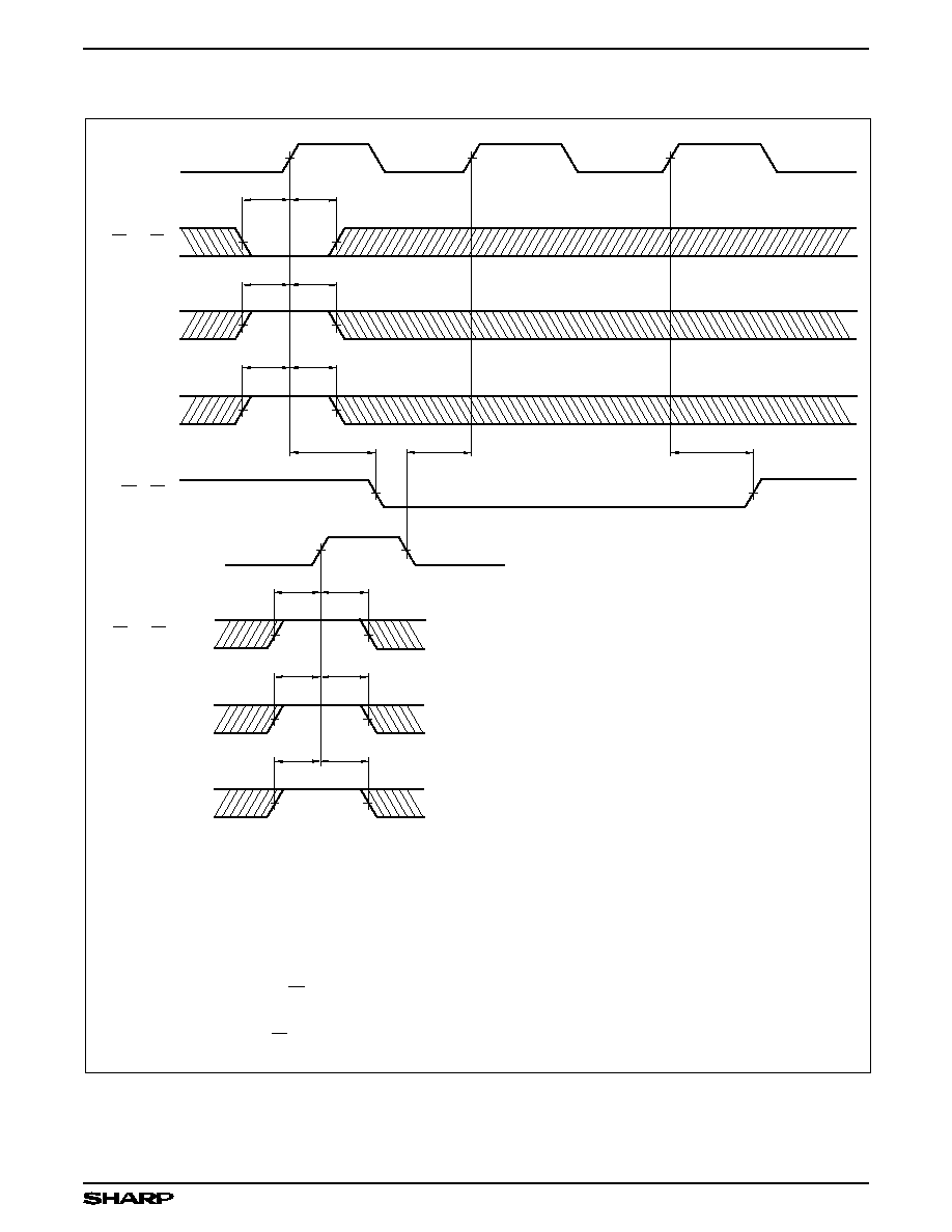
543611-46
CK
A
(CK
B
)
R/W
A
(R/W
B
)
R/W
B
(R/W
A
)
EN
B
(EN
A
)
t
RWS
t
ES
t
EH
t
RQS
t
RQH
t
FF
t
RWS
t
RWH
t
ES
t
EH
t
RQS
t
RQH
t
FF
t
SKEW1
(4)
t
RWH
REQ
B
(REQ
A
)
EN
A
(EN
B
)
REQ
A
(REQ
B
)
CK
B
(CK
A
)
FF
1
(FF
2
)
NOTES:
1. A
2A
, A
1A
, and A
0A
all are held HIGH for FIFO access at Port A.
A
0B
is held HIGH for FIFO access at Port B.
2. Parameters without parentheses apply to FIFO #1 operation.
Parameters with parentheses apply to FIFO #2 operation.
3. Assertion of the Full Flags is controlled by rising clock edges;
whereas, internal deassertion of the Full Flags is controlled by
falling clock edges, and their external deassertion is controlled
by rising clock edges.
4. t
SKEW1
is the minimum time between a falling CK
B
(CK
A
) edge
and a rising CK
A
(CK
B
) edge for FF to change predictably during
the current clock cycle. If the time between the falling edge of
CK
B
(CK
A
) and the rising edge of CK
A
(CK
B
) is less than t
SKEW1
,
then it is not guaranteed that FF will change state until the next
following CK
A
(CK
B
) edge.
Figure 23. Full Flag Timing, When Synchronous
TIMING DIAGRAMS (cont'd)
512 x 36 x 2/1024 x 36 x 2 BiFIFOs
LH543611/21
35

TIMING DIAGRAMS (cont'd)
AF
1
(AF
2
)
EH
t
ES
t
AF
t
AF
t
CK (CK )
A
B
EN (EN )
A
B
CK (CK )
B
A
R/W (R/W )
A
B
R/W (R/W )
B
A
RWH
t
RWS
t
RWH
t
RWS
t
543611-29
NOTES:
1. A
2A
,
A
1A
,
and A
0A
all are held HIGH for FIFO access at Port A.
A
0B
is held HIGH for FIFO access at Port B.
2. Parameters without parentheses apply to FIFO #1 operation.
Parameters with parentheses apply to FIFO #2 operation.
3. Assertion of the Almost-Full Flags is controlled by rising clock
edges; whereas, deassertion of the Almost-Full Flags is controlled
by falling clock edges.
t
RQS
t
RQH
REQ
A
(REQ
B
)
EH
t
ES
t
EN (EN )
B
A
t
RQS
t
RQH
REQ
B
(REQ
A
)
Figure 24. Almost-Full Flag Timing, When Asynchronous
LH543611/21
512 x 36 x 2/1024 x 36 x 2 BiFIFOs
36

TIMING DIAGRAMS (cont'd)
543611-47
CK
A
(CK
B
)
R/W
A
(R/W
B
)
R/W
B
(R/W
A
)
EN
B
(EN
A
)
t
RWS
t
ES
t
EH
t
RQS
t
RQH
t
AF
t
RWS
t
RWH
t
ES
t
EH
t
RQS
t
RQH
t
AF
t
SKEW1
(4)
t
RWH
REQ
B
(REQ
A
)
EN
A
(EN
B
)
REQ
A
(REQ
B
)
CK
B
(CK
A
)
AF
1
(AF
2
)
NOTES:
1. A
2A
, A
1A
, and A
0A
all are held HIGH for FIFO access at Port A.
A
0B
is held HIGH for FIFO access at Port B.
2. Parameters without parentheses apply to FIFO #1 operation.
Parameters with parentheses apply to FIFO #2 operation.
3. Assertion of the Almost-Full Flags is controlled by rising clock
edges; whereas, internal deassertion of the Almost-Full Flags
is controlled by falling clock edges, and their external deassertion
is controlled by rising clock edges.
4. t
SKEW1
is the minimum time between a falling CK
B
(CK
A
) edge
and a rising CK
A
(CK
B
) edge for AF to change predictably during
the current clock cycle. If the time between the falling edge of
CK
B
(CK
A
) and the rising edge of CK
A
(CK
B
) is less than t
SKEW1
,
then it is not guaranteed that AF will change state until the next
following CK
A
(CK
B
) edge.
Figure 25. Almost-Full Flag Timing, When Synchronous
512 x 36 x 2/1024 x 36 x 2 BiFIFOs
LH543611/21
37

TIMING DIAGRAMS (cont'd)
HF
1
(HF
2
)
EH
t
ES
t
HF
t
HF
t
CK (CK )
A
B
EN (EN )
A
B
CK (CK )
B
A
EH
t
ES
t
R/W (R/W )
A
B
R/W (R/W )
B
A
EN (EN )
B
A
RWH
t
RWS
t
RWH
t
RWS
t
543611-30
NOTES:
1. A
2A
,
A
1A
,
and A
0A
all are held HIGH for FIFO access at Port A.
A
0B
is held HIGH for FIFO access at Port B.
2. Parameters without parentheses apply to FIFO #1 operation.
Parameters with parentheses apply to FIFO #2 operation.
3. Both assertion and deassertion of the Half-Full Flags are controlled
entirely by rising clock edges, rather than by falling clock edges.
t
RQS
t
RQH
REQ
A
(REQ
B
)
t
RQS
t
RQH
REQ
B
(REQ
A
)
Figure 26. Half-Full Flag Timing, When Asynchronous
LH543611/21
512 x 36 x 2/1024 x 36 x 2 BiFIFOs
38

543611-48
CK
A
(CK
B
)
R/W
A
(R/W
B
)
R/W
B
(R/W
A
)
EN
B
(EN
A
)
t
RWS
t
ES
t
EH
t
RQS
t
RQH
t
HF
t
RWS
t
RWH
t
ES
t
EH
t
RQS
t
RQH
t
HF
t
SKEW2
(4)
t
RWH
REQ
B
(REQ
A
)
EN
A
(EN
B
)
REQ
A
(REQ
B
)
CK
B
(CK
A
)
HF
2
(HF
1
)
NOTES:
1. A
2A
, A
1A
, and A
0A
all are held HIGH for FIFO access at Port A.
A
0B
is held HIGH for FIFO access at Port B.
2. Parameters without parentheses apply to FIFO #2 operation.
Parameters with parentheses apply to FIFO #1 operation.
3. Both assertion and deassertion of the Half-Full Flags are controlled
entirely by rising clock edges, rather than by falling clock edges.
4. t
SKEW2
is the minimum time between a falling CK
B
(CK
A
) edge
and a rising CK
A
(CK
B
) edge for HF to change predictably during
the current clock cycle. If the time between the falling edge of
CK
B
(CK
A
) and the rising edge of CK
A
(CK
B
) is less than t
SKEW2
,
then it is not guaranteed that HF will change state until the next
following CK
A
(CK
B
) edge.
Figure 27. Half-Full Flag Timing, When Synchronized
to a Port Clock Doing Reading
TIMING DIAGRAMS (cont'd)
512 x 36 x 2/1024 x 36 x 2 BiFIFOs
LH543611/21
39
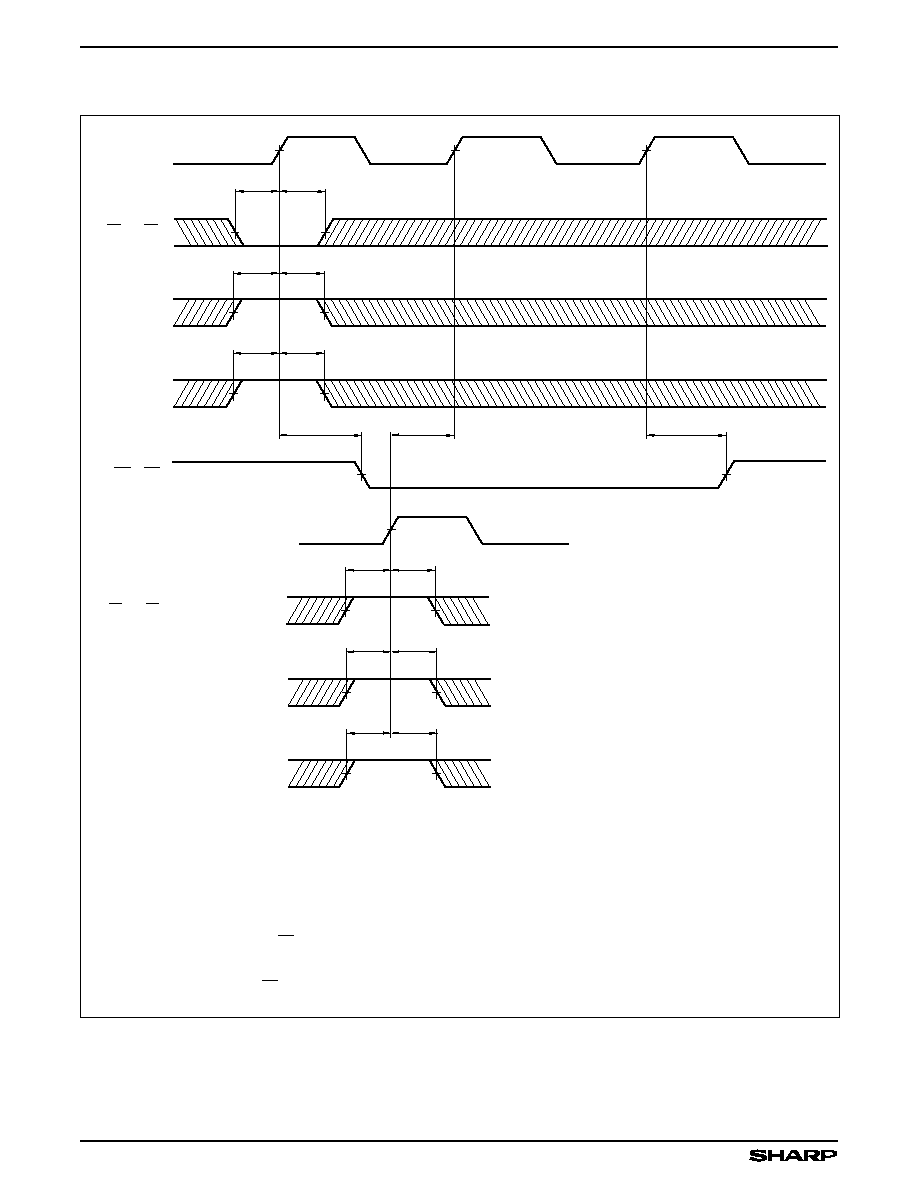
543611-49
CK
A
(CK
B
)
R/W
A
(R/W
B
)
R/W
B
(R/W
A
)
EN
B
(EN
A
)
t
RWS
t
ES
t
EH
t
RQS
t
RQH
t
HF
t
RWS
t
RWH
t
ES
t
EH
t
RQS
t
RQH
t
HF
t
SKEW1
(4)
t
RWH
REQ
B
(REQ
A
)
EN
A
(EN
B
)
REQ
A
(REQ
B
)
CK
B
(CK
A
)
HF
1
(HF
2
)
NOTES:
1. A
2A
, A
1A
, and A
0A
all are held HIGH for FIFO access at Port A.
A
0B
is held HIGH for FIFO access at Port B.
2. Parameters without parentheses apply to FIFO #1 operation.
Parameters with parentheses apply to FIFO #2 operation.
3. Both assertion and deassertion of the Half-Full Flags are
controlled entirely by rising clock edges, rather than by falling clock edges.
4. t
SKEW1
is the minimum time between a falling CK
B
(CK
A
) edge
and a rising CK
A
(CK
B
) edge for HF to change predictably during
the current clock cycle. If the time between the falling edge of
CK
B
(CK
A
) and the rising edge of CK
A
(CK
B
) is less than t
SKEW1
,
then it is not guaranteed that HF will change state until the next
following CK
A
(CK
B
) edge.
Figure 28. Half-Full Flag Timing, When Synchronized
to a Port Clock Doing Writing
TIMING DIAGRAMS (cont'd)
LH543611/21
512 x 36 x 2/1024 x 36 x 2 BiFIFOs
40
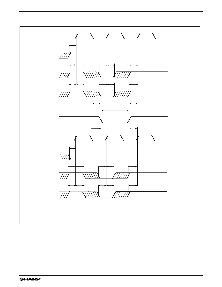
A
CK
A
R/W
RT
2
CK
B
B
R/W
EN
A
t
RSH
t
RS
t
RSH
t
RSS
t
ES
t
EH
t
ES
t
EH
t
ES
t
RSS
RWS
t
RWS
t
NOTES:
1. t
RSS
and t
RSH
need not be met unless a rising edge of CK
A
or CK
B
occurs while that clock is enabled.
2. t
RSS
is the time needed to deassert RT
2
before returning to a normal FIFO cycle.
3. t
RSH
is the time needed before asserting RT
2
after a normal FIFO cycle.
4. Read and write operations to FIFO #2 should be disabled while RT
2
is being asserted.
543611-31
t
RQS
t
RQH
t
RQS
t
RQH
t
RQS
EN
B
ES
t
EH
t
ES
t
EH
t
ES
t
REQ
A
REQ
B
t
RQS
t
RQH
t
RQS
t
RQH
t
RQS
Figure 29. FIFO #2 Retransmit
TIMING DIAGRAMS (cont'd)
512 x 36 x 2/1024 x 36 x 2 BiFIFOs
LH543611/21
41
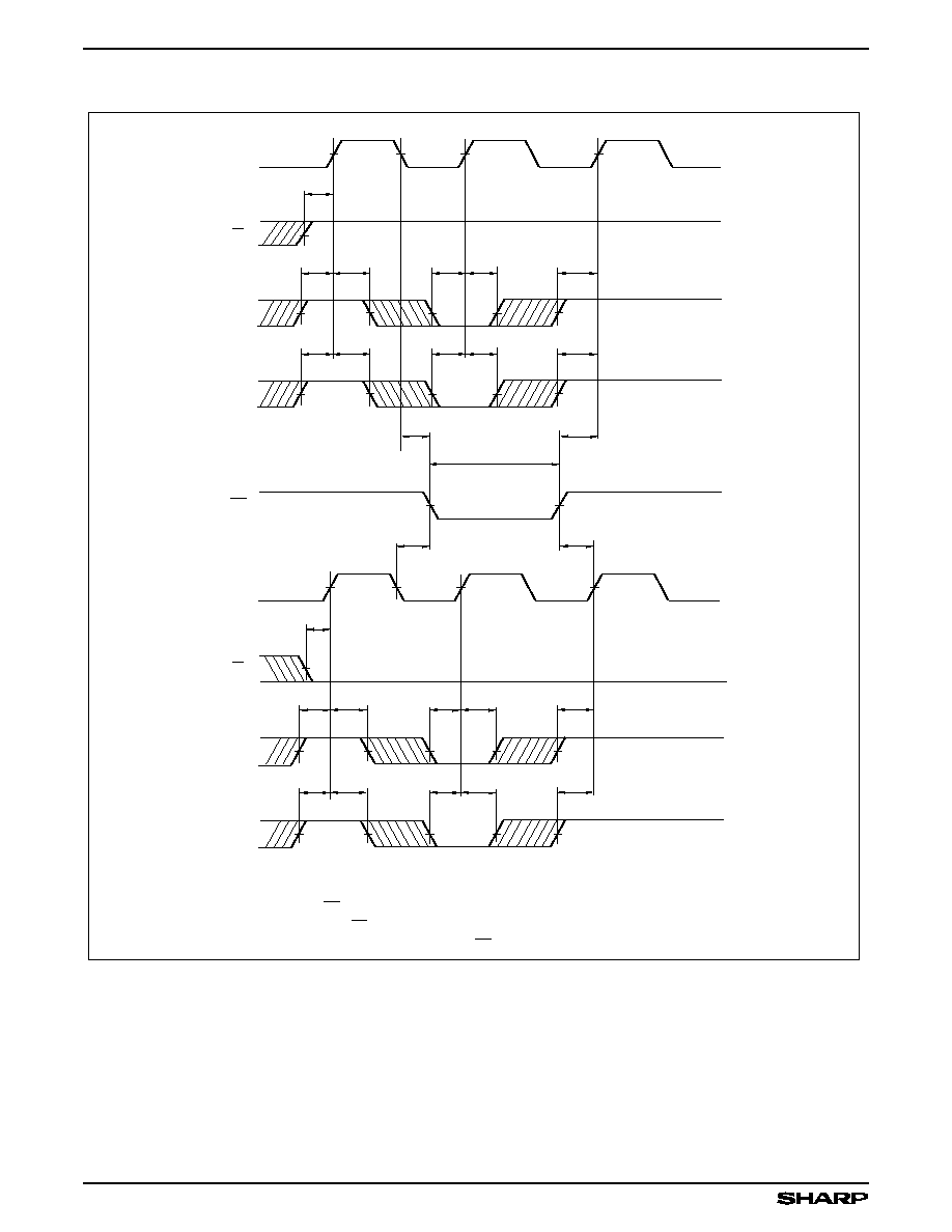
TIMING DIAGRAMS (cont'd)
B
CK
B
R/W
RT
1
CK
A
R/W
EN
B
t
RS
t
RSS
A
t
RSS
t
ES
t
EH
t
ES
t
EH
t
ES
t
RSH
RWS
t
RWS
t
NOTES:
1. t
RSS
and t
RSH
need not be met unless a rising edge of CK
A
or CK
B
occurs while that clock is enabled.
2. t
RSS
is the time needed to deassert RT
1
before returning to a normal FIFO cycle.
3. t
RSH
is the time needed before asserting RT
1
after a normal FIFO cycle.
4. Read and write operations to FIFO #1 should be disabled while RT
1
is being asserted.
t
RSH
543611-32
t
RQS
t
RQH
REQ
B
t
RQS
t
RQH
t
RQS
EN
A
t
ES
t
EH
t
ES
t
ES
EH
t
REQ
A
t
RQS
t
RQH
t
RQS
t
RQH
t
RQS
Figure 30. FIFO #1 Retransmit
LH543611/21
512 x 36 x 2/1024 x 36 x 2 BiFIFOs
42

TIMING DIAGRAMS (cont'd)
A
CK
A
R/W
A
EN
EF
1
B
CK
R/W
B
PREVIOUS DATA
t
EH
t
ES
t
EH
t
ES
t
DS
t
DH
t
DS
t
DH
t
OH
A
t
t
OH
A
t
EF
t
N1
N2
N1
N2
FRL
t
EF
t
NOTES:
1. A
2A
, A
1A
, A
0A
, and A
0B
are all held HIGH for FIFO access.
2. OE
A
is held HIGH.
3. OE
B
is held LOW.
4. t
FRL
(First Read Latency) - The first read following an empty condition
may begin no earlier than t
FRL
after the first write to an empty FIFO,
to ensure that valid read data is retrieved.
D
0A
- D
35A
D
0B
- D
35B
RWH
t
RWS
t
RWH
t
RWS
t
RWH
t
RWS
t
RWH
t
RWS
t
543611-33
t
RQS
t
RQH
REQ
A
t
RQS
t
RQH
B
EN
ES
t
EH
t
t
EH
ES
t
t
RQS
t
RQH
REQ
B
t
RQS
t
RQH
Figure 31. FIFO #1 Write and Read Operation in
Near-Empty Region
512 x 36 x 2/1024 x 36 x 2 BiFIFOs
LH543611/21
43

TIMING DIAGRAMS (cont'd)
B
CK
B
R/W
B
EN
EF
2
A
CK
R/W
A
A
EN
t
EH
t
ES
t
EH
t
ES
t
DS
t
DH
t
DS
t
DH
t
EH
ES
t
EH
t
ES
t
EF
t
FRL
t
EF
t
NOTES:
1. A
2A
, A
1A
, A
0A
, and A
0B
are all held HIGH for FIFO access.
2. OE
B
is held HIGH.
3. OE
A
is held LOW.
4. t
FRL
(First Read Latency) - The first read following an empty condition
may begin no earlier than t
FRL
after the first write to an empty FIFO,
to ensure that valid read data is retrieved.
t
A
t
A
t
OH
t
OH
D
0B
- D
35B
D
0A
- D
35A
RWH
t
RWS
t
RWH
t
RWS
t
RWH
t
RWS
t
RWH
t
RWS
t
PREVIOUS DATA
N1
N2
N1
N2
543611-34
t
RQS
t
RQH
REQ
B
t
RQS
t
RQH
REQ
A
t
RQS
t
RQH
t
RQH
t
RQS
Figure 32. FIFO #2 Write and Read Operation in
Near-Empty Region
LH543611/21
512 x 36 x 2/1024 x 36 x 2 BiFIFOs
44
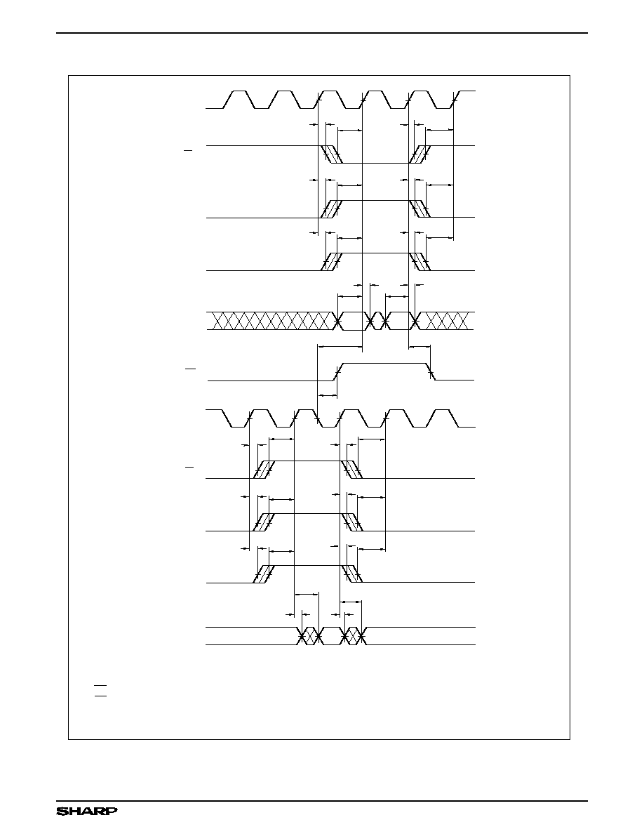
TIMING DIAGRAMS (cont'd)
A
CK
A
R/W
FF
1
B
CK
R/W
B
PREVIOUS DATA
t
DS
t
DH
t
DS
t
DH
t
FWL
t
FF
t
OH
A
t
t
OH
A
t
FF
t
NOTES:
1. A
2A
,
A
1A
,
and A
0A
all are held HIGH for FIFO access at Port A.
A
0B
is held HIGH for FIFO access at Port B.
2. OE
A
is held HIGH.
3. OE
B
is held LOW.
4. t
FWL
(First Write Latency) - The first write following a full condition
may begin no earlier than t
FWL
after the first read from a full FIFO,
to ensure that valid write data is written.
D
0A
- D
35A
D
0B
- D
35B
RWH
t
RWS
t
RWH
t
RWS
t
RWH
t
RWS
t
RWH
t
RWS
t
543611-35
A
EN
t
EH
t
ES
t
EH
t
ES
t
RQS
t
RQH
REQ
A
t
RQS
t
RQH
B
EN
ES
t
EH
t
t
EH
ES
t
t
RQS
t
RQH
REQ
B
t
RQS
t
RQH
Figure 33. FIFO #1 Read and Write Operation in
Near-Full Region
512 x 36 x 2/1024 x 36 x 2 BiFIFOs
LH543611/21
45

TIMING DIAGRAMS (cont'd)
B
CK
B
R/W
FF
2
A
CK
R/W
A
A
EN
NOTES:
1. A
2A
,
A
1A
,
and A
0A
all are held HIGH for FIFO access at Port A.
A
0B
is held HIGH for FIFO access at Port B.
2. OE
B
is held HIGH.
3. OE
A
is held LOW.
4. t
FWL
(First Write Latency) - The first write following a full condition
may begin no earlier than t
FWL
after the first read from a full FIFO,
to ensure that valid write data is written.
D
0B
- D
35B
D
0A
- D
35A
PREVIOUS DATA
t
DS
t
DH
t
DS
t
DH
t
FWL
t
FF
ES
t
EH
t
t
EH
ES
t
t
OH
A
t
t
OH
A
t
FF
t
RWH
t
RWS
t
RWH
t
RWS
t
RWH
t
RWS
t
RWH
t
RWS
t
543611-36
B
EN
t
EH
t
ES
t
EH
t
ES
t
RQS
t
RQH
REQ
B
t
RQS
t
RQH
t
RQS
t
RQH
REQ
A
t
RQS
t
RQH
Figure 34. FIFO #2 Read and Write Operation in
Near-Full Region
LH543611/21
512 x 36 x 2/1024 x 36 x 2 BiFIFOs
46

TIMING DIAGRAMS (cont'd)
t
ES
B
CK
B
R/W
B
EN
t
A
WORD # n+1
WORD # n
NOTES:
1. A
0B
is held HIGH for FIFO access.
2. OE
B
is held LOW.
3. WS
0
is held HIGH and WS
1
is held LOW for double-byte access.
4. Data-access time t
A
, after the rising edge of CK
B
, shown for the
first read cycle, applies similarly for all subsequent read cycles.
D
0B
- D
17B
D
18B
- D
35B
RWS
t
WORD # n+2
WORD # n+1
WORD # n
WORD # n+2
BITS
0-17
BITS
18-35
BITS
0-17
BITS
18-35
BITS
0-17
BITS
18-35
BITS
0-17
BITS
18-35
BITS
0-17
BITS
18-35
543611-37
t
RQS
B
REQ
Figure 35. Port B Double-Byte FIFO #1 Read Access for
36-to-18 Funneling
512 x 36 x 2/1024 x 36 x 2 BiFIFOs
LH543611/21
47

B
CK
B
R/W
t
DS
t
DH
WORD # n
WORD # n+1
WORD # n+2
NOTES:
1. A
0B
is held HIGH for FIFO access.
2. OE
B
is held HIGH.
3. WS
0
is held HIGH and WS
1
is held LOW for double-byte access.
4. Data-setup time t
DS
and data-hold time t
DH
, before and after
the rising edge of CK
B
, shown for the first write cycle, apply
similarly for all subsequent write cycles.
D
0B
- D
17B
RWS
t
BITS
0-17
BITS
18-35
BITS
0-17
BITS
18-35
BITS
0-17
BITS
18-35
543611-38
t
ES
B
EN
t
RQS
B
REQ
Figure 36. Port B Double-Byte FIFO #2 Write Access for
18-to-36 Defunneling
TIMING DIAGRAMS (cont'd)
LH543611/21
512 x 36 x 2/1024 x 36 x 2 BiFIFOs
48
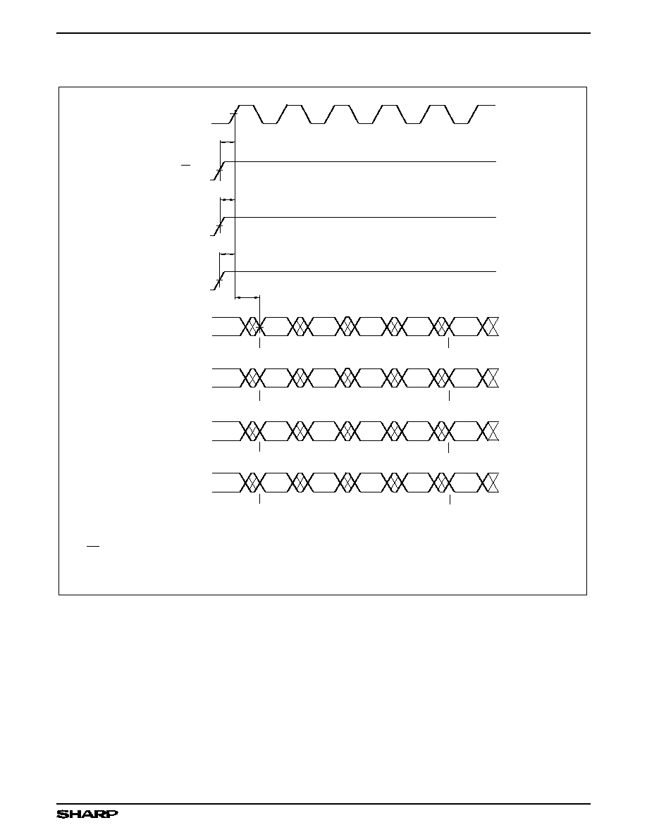
TIMING DIAGRAMS (cont'd)
t
ES
B
CK
B
R/W
B
EN
BITS
0-8
t
A
WORD # n+1
WORD # n
NOTES:
1. A
0B
is held HIGH for FIFO access.
2. OE
B
is held LOW.
3. WS
0
and WS
1
both are held LOW for single-byte access.
4. Data-access time t
A
, after the rising edge of CK
B
, shown for the
first read cycle, applies similarly for all subsequent read cycles.
BITS
9-17
BITS
18-26
BITS
27-35
BITS
0-8
BITS
9-17
BITS
18-26
BITS
27-35
BITS
0-8
BITS
9-17
BITS
18-26
BITS
27-35
BITS
0-8
BITS
9-17
BITS
18-26
BITS
27-35
BITS
0-8
BITS
9-17
BITS
18-26
BITS
27-35
D
27B
- D
35B
D
18B
- D
26B
D
9B
- D
17B
D
0B
- D
8B
RWS
t
WORD # n+1
WORD # n
WORD # n+1
WORD # n
WORD # n+1
WORD # n
543611-39
t
RQS
B
REQ
Figure 37. Port B Single-Byte FIFO #1 Read Access for
36-to-9 Funneling
512 x 36 x 2/1024 x 36 x 2 BiFIFOs
LH543611/21
49
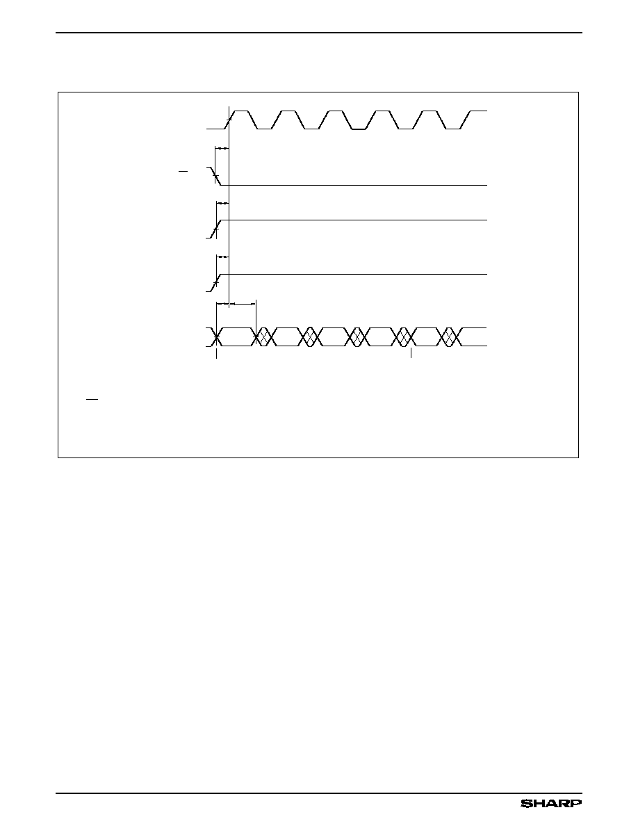
TIMING DIAGRAMS (cont'd)
t
ES
B
CK
B
R/W
B
EN
BITS
0-8
BITS
9-17
BITS
18-26
BITS
27-35
t
DS
t
DH
WORD # n
WORD # n+1
NOTES:
1. A
0B
is held HIGH for FIFO access.
2. OE
B
is held HIGH.
3. WS
0
and WS
1
both are held LOW for single-byte access.
4. Data-setup time t
DS
and data-hold time t
DH
, before and after
the rising edge of CK
B
, shown for the first write cycle, apply
similarly for all subsequent write cycles.
BITS
0-8
BITS
9-17
D
0B
- D
8B
RWS
t
543611-40
t
RQS
B
REQ
Figure 38. Port B Single-Byte FIFO #2 Write Access for
LH543611/21
512 x 36 x 2/1024 x 36 x 2 BiFIFOs
50

543611-41
t
RQS
t
ACK
t
AF
t
ACK
t
ACK
t
ACK
B
(CK )
B
(R/W )
B
(REQ )
B
(ACK )
(AF
2
)
A
CK
A
R/W
A
REQ
A
ACK
AF
1
RWS
t
*
*
*
*
*
*
Indicates where a write would take place, if ACK were tied to EN.
NOTES:
1. For a FIFO access to occur, REQ and EN must be held HIGH for the required setup and hold times.
2. ACK can be tied directly to EN to directly gate FIFO accesses.
3. REQ must be maintained HIGH with R/W stable throughout entire clock cycle for ACK to be generated.
4. When the REQ/ACK handshake is not used, ACK can be ignored,
and REQ may be tied HIGH or used as a second enable.
5. Parameters without parentheses apply to Port A. Parameters with parentheses apply to Port B.
Starting at the third cycle after entering the
'almost-full' region, acknowledge
occurs on every third cycle to prevent overrun
of the full condition.
Outside the 'almost-full' region,
acknowledge is continuous
for a continuous request.
1
2
Figure 39. Write Request/Acknowledge Handshake
TIMING DIAGRAMS (cont'd)
512 x 36 x 2/1024 x 36 x 2 BiFIFOs
LH543611/21
51
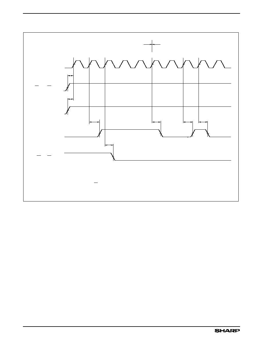
TIMING DIAGRAMS (cont'd)
t
RQS
t
ACK
t
AE
t
ACK
t
ACK
t
ACK
B
(CK )
B
(R/W )
B
(REQ )
B
(ACK )
(AE
1
)
A
CK
A
R/W
A
REQ
A
ACK
AE
2
RWS
t
Starting at the third cycle after entering the
'almost-empty' region, acknowledge
occurs on every third cycle to prevent underrun
of the empty condition.
Outside the 'almost-empty' region,
acknowledge is continuous
for a continuous request.
*
Indicates where a read would take place, if ACK were tied to EN.
NOTES:
1. For a FIFO access to occur, REQ and EN must be held HIGH for the required setup and hold times.
2. ACK can be tied directly to EN to directly gate FIFO accesses.
3. REQ must be maintained HIGH with R/W stable throughout entire clock cycle for ACK to be generated.
4. When the REQ/ACK handshake is not used, ACK can be ignored,
and REQ may be tied HIGH or used as a second enable.
5. Parameters without parentheses apply to Port A. Parameters with parentheses apply to Port B.
*
*
*
*
*
543611-42
1
2
Figure 40. Read Request/Acknowledge Handshake
LH543611/21
512 x 36 x 2/1024 x 36 x 2 BiFIFOs
52

t
RWS
t
ES
t
RQS
t
WSS
t
WSH
t
WSS
t
WSH
t
PF
t
DH
t
DS
t
PF
t
A
t
PF
CK
B
R/W
B
EN
B
REQ
B
WS
1
WS
0
PF
B
D
0B
- D
35B
PF
B
D
0B
- D
35B
PF
B
(WHEN DATA
WORDS ARE
INCOMING)
(SYNCHRONOUS
LATCHING)
(ASYNCHRONOUS,
WHEN DATA WORDS
ARE INCOMING)
(WHEN DATA
WORDS ARE
OUTGOING)
(ASYNCHRONOUS,
WHEN DATA WORDS
ARE OUTGOING)
543611-50
NOTE: During retransmit, WS
1
and WS
0
must be stable throughout entire clock cycle.
Figure 41. Changing Port B
Word-Width Selection During Operation
TIMING DIAGRAMS (cont'd)
512 x 36 x 2/1024 x 36 x 2 BiFIFOs
LH543611/21
53
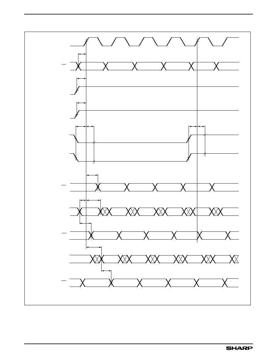
t
RWS
t
ES
t
RQS
t
WSS
t
WSH
t
WSS
t
WSH
t
PF
t
DH
t
DS
t
PF
t
A
t
PF
CK
B
R/W
B
EN
B
REQ
B
WS
1
WS
0
PF
B
D
0B
- D
35B
PF
B
D
0B
- D
35B
PF
B
(WHEN DATA WORDS
ARE INCOMING)
(SYNCHRONOUS
LATCHING)
(ASYNCHRONOUS,
WHEN DATA WORDS
ARE INCOMING)
(WHEN DATA
WORDS ARE
OUTGOING)
(ASYNCHRONOUS,
WHEN DATA WORDS
ARE OUTGOING)
543611-51
NOTE: During parity mode changes (odd or even), T
PF
may have additional delay from the rising edge of the clock.
Figure 42. Parity Generation
TIMING DIAGRAMS (cont'd)
LH543611/21
512 x 36 x 2/1024 x 36 x 2 BiFIFOs
54

PACKAGE DIAGRAMS
132PQFP
DIMENSIONS IN MM [INCHES]
MAXIMUM LIMIT
MINIMUM LIMIT
132PQFP (PQFP132-P-S950)
28.02 [1.103]
27.86 [1.097]
0.635
[0.025] TYP
NON-ACCUM
4.57 [0.180]
4.06 [0.160]
0.51 [0.020]
MIN.
24.21 [0.953]
24.05 [0.947]
28.02 [1.103]
27.86 [1.097]
27.69 [1.090]
27.18 [1.070]
27.69 [1.090]
27.18 [1.070]
SECTION
0.10 [0.004]
0.51 [0.020] MIN.
0.15 [0.006]
0
∞
- 8
∞
45
∞
CHAMFER
TOP VIEW
24.21 [0.953]
24.05 [0.947]
0.25 [0.010] TYP.
132-pin PQFP
512 x 36 x 2/1024 x 36 x 2 BiFIFOs
LH543611/21
55

DIMENSIONS IN MM [INCHES]
MAXIMUM LIMIT
MINIMUM LIMIT
144TQFP (TQFP-144-P-2020)
0.50 [0.020]
TYP.
0.20 [0.008]
0.09 [0.004]
20.0 [0.787]
BASIC
144TQFP
1.45 [0.057]
1.35 [0.053]
DETAIL
20.0
[0.787]
BASIC
1.60 [0.063]
REF. MAX
0.15 [0.006]
0.05 [0.002]
22.0
[0.866]
BASIC
0.27 [0.010]
0.17 [0.007]
22.0 [0.866]
BASIC
0.75 [0.030]
0.47 [0.019]
1.00
[0.039]
REF.
144-pin TQFP
LH543611/21
512 x 36 x 2/1024 x 36 x 2 BiFIFOs
56

ORDERING INFORMATION
15
20
25
30
35
Cycle Times (ns)
M 144-pin, Thin Quad Flat Package (TQFP144-P-2020)
P 132-pin, Plastic Quad Flat Package (PQFP132-P-S950)
LH543611/21
Device Type
X
Package
- ##
Speed
512 x 36 x 2/1K x 36 x 2 Bidirectional FIFO
Example: LH543611M-15 (512 x 36 x 2 Bidirectional FIFO, 15 ns, 144-pin, Thin Quad Flat Package)
543611-43
NOTE:
For PQFP-to-PGA conversion for through-hole board designs, SHARP recommends QFP-to-PGA adaptors from ISI (Interconnect Systems Inc.)
ISI makes three models that can map the LH543611/21 132-pin PQFP to a 13x13 PGA (100 mil); mode #A 13225-1Æ map to a SHARP spe-
cific 120-pin PGA. For more information, contact SHARP or ISI directly at P.O. Box 1089, Simi Valley, CA 93062, Tel: (805) 581-5626.
512 x 36 x 2/1024 x 36 x 2 BiFIFOs
LH543611/21
57