
LH5496/96H
CMOS 512
◊
9 FIFO
FEATURES
∑∑
Fast Access Times:
15 */20/25/35/50/65/80 ns
∑∑
Full CMOS Dual Port Memory Array
∑∑
Fully Asynchronous Read and Write
∑∑
Expandable-in Width and Depth
∑∑
Full, Half-Full, and Empty Status Flags
∑∑
Read Retransmit Capability
∑∑
TTL Compatible I/O
∑∑
Packages:
28-Pin, 300-mil PDIP
28-Pin, 600-mil PDIP
32-Pin PLCC
∑∑
Pin and Functionally Compatible with IDT7201
FUNCTIONAL DESCRIPTION
The LH5496/96H are dual port memories with internal
addressing to implement a First-In, First-Out algorithm.
Through an advanced dual port architecture, they provide
fully asynchronous read/write operation. Empty, Full, and
Half-Full status flags are provided to prevent data over-
flow and underflow. In addition, internal logic provides for
unlimited expansion in both word size and depth.
Read and write operations automatically access se-
quential locations in memory in that data is read out in the
same order that it was written, that is on a First-In,
First-Out basis. Since the address sequence is internally
predefined, no external address information is required
for the operation of this device. A ninth data bit is provided
for parity or control information often needed in commu-
nication applications.
Empty, Full, and Half-Full status flags monitor the
extent to which data has been written into the FIFO, and
prevent improper operations (i.e., Read if the FIFO is
empty, or Write if the FIFO is full). A retransmit feature
resets the Read address pointer to its initial position,
thereby allowing repetitive readout of the same data.
Expansion In and Expansion Out pins implement an
expansion scheme that allows individual FIFOs to be
cascaded to greater depth without incurring additional
latency (bubblethrough) delays.
PIN CONNECTIONS
5496-1D
1
2
3
4
5
6
7
8
9
10
11
12
13
14
W
D
8
D
3
D
2
D
1
D
0
XI
FF
Q
0
V
SS
28
27
26
25
24
23
22
21
20
19
18
17
16
15
V
CC
D
4
FL/RT
RS
EF
XO/HF
R
Q
1
Q
2
Q
3
Q
8
D
6
D
5
D
7
Q
7
Q
6
Q
5
Q
4
28-PIN PDIP
TOP VIEW
Figure 1. Pin Connections for PDIP Packages
5
6
7
8
9
10
D
2
D
1
D
0
XI
FF
Q
0
11
Q
1
2
3
4
32 31 30
29
28
27
26
25
24
D
6
D
7
NC
EF
D
3
D
8
W
NC
V
CC
D
4
D
5
14 15 16
20
19
18
17
FL/RT
RS
23
XO/HF
22
Q
7
21
Q
6
12
NC
13
Q
2
1
Q
3
Q
8
V
SS
NC
R
Q
4
Q
5
5496-2D
32-PIN PLCC
TOP VIEW
Figure 2. Pin Connections for PLCC Package
* LH5496 only.
1

PIN DESCRIPTIONS
PIN
PIN TYPE *
DESCRIPTION
D
0
≠ D
8
I
Input Data Bus
Q
0
≠ Q
8
O/Z
Output Data Bus
W
I
Write Request
R
I
Read Request
EF
O
Empty Flag
FF
O
Full Flag
* I = Input, O = Output, Z = High-Impedance, V = Power Voltage Level
PIN
PIN TYPE *
DESCRIPTION
XO/HF
O
Expansion Out/Half-Full Flag
XI
I
Expansion In
FL/RT
I
First Load/Retransmit
RS
I
Reset
V
CC
V
Positive Power Supply
V
SS
V
Ground
DATA OUTPUTS
Q
0
- Q
8
FLAG
LOGIC
WRITE
POINTER
READ
POINTER
DATA INPUTS
D
0
- D
8
DUAL-PORT
RAM
ARRAY
512 x 9
EF
FF
. . .
5496-3
INPUT
PORT
CONTROL
R
W
RESET
LOGIC
RS
OUTPUT
PORT
CONTROL
EXPANSION
LOGIC
XO/HF
XI
FL/RT
Figure 3. LH5496/96H Block Diagram
LH5496/96H
CMOS 512
◊
9 FIFO
2
ABSOLUTE MAXIMUM RATINGS
1
PARAMETER
RATING
Supply Voltage to V
SS
Potential
≠0.5 V to 7 V
Signal Pin Voltage to V
SS
Potential
3
≠0.5 V to V
CC
+ 0.5 V (not to exceed 7 V)
DC Output Current
2
±
50 mA
Storage Temperature Range
≠65
o
C to 150
o
C
Power Dissipation (Package Limit)
1.0 W
DC Voltage Applied To Outputs In High-Z State
≠0.5 V to Vcc + 0.5 V (not to exceed 7 V)
NOTES:
1.
Stresses greater than those listed under `Absolute Maximum Ratings' may cause permanent damage to the device.
This is a device stress rating for transient conditions only. Functional operation at these or any other conditions above
those indicated in the `Operating Range' of this specification is not implied. Exposure to absolute maximum rating
conditions for extended periods may affect reliability.
2.
Outputs should not be shorted for more than 30 seconds. No more than one output should be shorted at any time.
3.
Negative undershoots of 1.5 V in amplitude are permitted for up to 10 ns once per cycle.
OPERATING RANGE
SYMBOL
PARAMETER
MIN
MAX
UNIT
T
A
Temperature, Ambient, LH5496
0
70
o
C
T
A
Temperature, Ambient, LH5496H
≠ 40
85
o
C
V
CC
Supply Voltage
4.5
5.5
V
V
SS
Supply Voltage
0
0
V
V
IL
Logic `0' Input Voltage
1
≠0 .5
0.8
V
V
IH
Logic `1' Input Voltage
2.0
V
CC
+ 0.5
V
NOTE:
1.
Negative undershoots of 1.5 V in amplitude are permitted for up to 10 ns once per cycle.
DC ELECTRICAL CHARACTERISTICS (Over Operating Range)
SYMBOL
PARAMETER
TEST CONDITIONS
MIN
MAX
UNIT
I
LI
Input Leakage Current
V
CC
= 5.5 V, V
IN
= 0 V to V
CC
≠10
10
µ
A
I
LO
Output Leakage Current
R
V
IH
, 0 V
V
OUT
V
CC
≠10
10
µ
A
V
OH
Output High Voltage
I
OH
= ≠2.0 mA
2.4
V
V
OL
Output Low Voltage
I
OL
= 8.0 mA
0.4
V
I
CC
Average Supply Current
1
Measured at f = 40 MHz
100
mA
I
CC2
Average Standby Current
1
All Inputs = V
IH
15
mA
I
CC3
Power Down Current
1
All Inputs = V
CC
≠ 0.2 V
5
mA
NOTE:
1.
I
CC
, I
CC2
, and I
CC3
are dependent upon actual output loading and cycle rates. Specified values are with outputs open.
CMOS 512
◊
9 FIFO
LH5496/96H
3

AC TEST CONDITIONS
PARAMETER
RATING
Input Pulse Levels
V
SS
to 3 V
Input Rise and Fall Times (10% to 90%)
5 ns
Input Timing Reference Levels
1.5 V
Output Reference Levels
1.5 V
Output Load, Timing Tests
Figure 4
CAPACITANCE
1,2
PARAMETER
RATING
C
IN
(Input Capacitance)
5 pF
C
OUT
(Output Capacitance)
7 pF
NOTES:
1.
Sample tested only.
2.
Capacitances are maximum values at 25
o
C measured at 1.0 MHz
with V
IN
= 0 V.
5496-4
DEVICE
UNDER
TEST
+5 V
30 pF
1.1 k
680
INCLUDES JIG & SCOPE CAPACITANCES
*
*
Figure 4. Output Load Circuit
LH5496/96H
CMOS 512
◊
9 FIFO
4

AC ELECTRICAL CHARACTERISTICS
1
(Over Operating Range)
SYMBOL
PARAMETER
t
A
= 15 ns
2
t
A
= 20 ns t
A
= 25 ns t
A
= 35 ns t
A
= 50 ns t
A
= 65 ns
t
A
= 80 ns
UNIT
MIN
MAX MIN MAX MIN MAX MIN MAX MIN MAX MIN
MAX
MIN MAX
READ CYCLE TIMING
t
RC
Read
Cycle
Time
25
≠
30
≠ 35
≠ 45
≠
65
≠ 80
≠
100
≠
ns
t
A
Access Time
≠
15
≠
20
≠
25
≠
35
≠
50
≠
65
≠
80
ns
t
RR
Read
Recover
Time
10
≠
10
≠ 10
≠
10
≠
15
≠ 15
≠
15
≠
ns
t
RPW
Read Pulse Width
3
15
≠
20 ≠ 25
≠
35
≠
50
≠ 65
≠
80
≠
ns
t
RLZ
Data Bus Active from Read LOW
4
5
≠
5
≠
5
≠
5
≠
5
≠
5
≠
10
≠
ns
t
WLZ
Data Bus Active from Write
HIGH
4,5
10
≠
10
≠ 10
≠
10
≠
10
≠ 10
≠
20
≠
ns
t
DV
Data Valid from Read Pulse HIGH
5
≠
5
≠
5
≠
5
≠
5
≠
5
≠
5
≠
ns
t
RHZ
Data Bus High-Z from Read
HIGH
4
≠
15
≠
15
≠
15
≠
15
≠
20
≠
30
≠
30
ns
WRITE CYCLE TIMING
t
WC
Write Cycle Time
25
≠
30
≠
35
≠
45
≠
65
≠
80
≠
100
≠
ns
t
WPW
Write Pulse Width
3
15
≠
20
≠ 25
≠
35
≠
50
≠
65
≠ 80
≠
ns
t
WR
Write
Recovery
Time
10
≠
10
≠ 10
≠
10
≠
15
≠
15
≠ 15
≠
ns
t
DS
Data Setup Time
10
≠
10
≠
10
≠
15
≠
20
≠
20
≠
20
≠
ns
t
DH
Data
Hold
Time
0
≠
0
≠ 0
≠
0
≠
0
≠
5
≠ 5
≠
ns
RESET TIMING
t
RSC
Reset Cycle Time
25
≠
30
≠
35
≠
45
≠
65
≠
80
≠
100
≠
ns
t
RS
Reset Pulse Width
3
15
≠
20
≠ 25
≠
35
≠
50
≠
65
≠
80
≠
ns
t
RSR
Reset Recovery Time
10
≠
10
≠
10
≠
10
≠
15
≠
15
≠
15
≠
ns
t
RRSS
Read HIGH to RS HIGH
15
≠
20
≠
25
≠
35
≠
50
≠
65
≠
80
≠
ns
t
WRSS
Write HIGH to RS HIGH
15
≠
20
≠
25
≠
35
≠
50
≠
65
≠
80
≠
ns
RETRANSMIT TIMING
t
RTC
Retransmit Cycle Time
25
≠
30
≠ 35
≠ 45
≠
65
≠
80
≠
100
≠
ns
t
RT
Retransmit Pulse Width
3
15
≠
20
≠ 25
≠ 35
≠
50
≠
65
≠
80
≠
ns
t
RTR
Retransmit
Recovery
Time
10
≠
10
≠ 10
≠ 10
≠
15
≠
15
≠
15
≠
ns
FLAG TIMING
t
EFL
Reset LOW to Empty Flag LOW
≠
25
≠
30
≠
35
≠
45
≠
65
≠
80
≠
100
ns
t
HFH,FFH
Reset LOW to Half-Full and Full
Flags HIGH
≠
25
≠
30
≠
35
≠
45
≠
65
≠
80
≠
100
ns
t
REF
Read LOW to Empty Flag LOW
≠
20
≠
25
≠
25
≠
35
≠
45
≠
60
≠
60
ns
t
RFF
Read HIGH to Full Flag HIGH
≠
20
≠
25
≠
25
≠
35
≠
45
≠
60
≠
60
ns
t
WEF
Write HIGH to Empty Flag HIGH
≠
20
≠
25
≠
25
≠
35
≠
45
≠
60
≠
60
ns
t
WFF
Write LOW to Full Flag LOW
≠
20
≠
25
≠
25
≠
35
≠
45
≠
60
≠
60
ns
t
WHF
Write LOW to Half-Full Flag LOW
≠
25
≠
30
≠
35
≠
45
≠
65
≠
80
≠
100
ns
t
RHF
Read HIGH to Half-Full Flag HIGH
≠
25
≠
30
≠
35
≠
45
≠
65
≠
80
≠
100
ns
EXPANSION TIMING
t
XOL
Expansion Out LOW
≠
18
≠
20
≠
25
≠
35
≠
50
≠
65
≠
80
ns
t
XOH
Expansion Out HIGH
≠
18
≠
20
≠
25
≠
35
≠
50
≠
65
≠
80
ns
t
XI
Expansion In Pulse Width
15
≠
20
≠
25
≠
35
≠
50
≠
65
≠
80
≠
ns
t
XIR
Expansion In Recovery Time
10
≠
10
≠
10
≠
10
≠
10
≠
10
≠
10
≠
ns
t
XIS
Expansion in Setup Time
7
≠
10
≠
10
≠
15
≠
15
≠
15
≠
15
≠
ns
NOTES:
1.
LH5496 only.
2.
All timing measurements performed at `AC Test Condition' levels.
CMOS 512
◊
9 FIFO
LH5496/96H
5

OPERATIONAL DESCRIPTION
Reset
The device is reset whenever the Reset pin (RS) is
taken to a LOW state. The reset operation initializes both
the read and write address pointers to the first memory
location. The XI and FL pins are also sampled at this time
to determine whether the device is in Single mode or
Depth Expansion mode. A reset pulse is required when
the device is first powered up. The Read (R) and Write
(W) pins may be in any state when reset is initiated, but
must be brought to a HIGH state t
RPW
and t
WPW
before
the rising edge of RS. The reset operation forces the
Empty Flag EF to be asserted (EF = LOW), and the
Half-Full Flag HF and the Full FLag FF to be deasserted
(HF = FF = HIGH); the Data Out pins (D
0
≠ D
8
) are forced
into a high-impedance state.
Write
A write cycle is initiated on the falling edge of the Write
(W) pin. Data setup and hold times must be observed on
the data in (D
0
≠ D
8
) pins. A write operation is only possible
if the FIFO is not full, (i.e. the Full flag pin is HIGH). Writes
may occur independently of any ongoing read operta-
tions.
At the falling edge of the first write after the memory is
half filled, the Half-Full flag will be asserted (HF = LOW)
and will remain asserted until the difference between the
write pointer and read pointer indicates that the remaining
data in the device is less than or equal to one half the total
capacity of the FIFO. The Half-Full flag is deasserted
(HF = HIGH) by the appropriate rising edge of R.
The Full flag is asserted (FF = LOW) at the falling edge
of the write operation which fills the last available location
in the FIFO memory array. The Full flag will inhibit further
writes until cleared by a valid read. The Full flag is
deasserted (FF = HIGH) after the next rising edge of R
releases another memory location.
Read
A read cycle is initiated on the falling edge of the Read
(R) pin. Read data becomes valid on the data out (Q
0
≠Q
8
)
pins after a time t
A
from the falling edge of R. After R goes
HIGH, the data out pins return to a high-impedance state.
Reads may occur independent of any ongoing write
operations. A read is only possible if the FIFO is not empty
(EF = HIGH).
The internal read and write address pointers are main-
tained by the device such that consecutive read opera-
tions will access data in the same order as it was written.
The Empty flag is asserted (EF = LOW) after the falling
edge of R which accesses the last available data in the
FIFO memory. EF is deasserted (EF = HIGH) after the
next rising edge of W loads another word of valid data.
Data Flow-Through
Read flow-through mode occurs when the Read (R)
pin is brought LOW while the FIFO is empty, and held
LOW in anticipation of a write cycle. At the end of the next
write cycle, the Empty flag will be momentarily deas-
serted, and the data just written will become available on
the data out pins after a maximum time of t
WEF
+ t
A
.
Additional writes may occur while the R pin remains LOW,
but only data from the first write flows through to the
outputs. Additional data, if any, can only be accessed by
toggling R.
Write flow-through mode occurs when the Write (W)
pin is brought LOW while the FIFO is full, and held LOW
in anticipation of a read cycle. At the end of the read cycle,
the Full flag will be momentarily deasserted, but then
immediately reasserted in response to W held LOW. Data
is written into the FIFO on the rising edge of W which may
occur t
RFF
+ t
WPW
after the read.
Retransmit
The FIFO can be made to reread previously read data
through the retransmit function. Retransmit is initiated by
pulsing RT LOW. This resets the internal read address
pointer to the first physical location in the memory while
leaving the internal write address pointer unchanged.
Data between the read and write pointers may be reac-
cessed by subsequent reads. Both R and W must be
inactive (HIGH) during the retransmit pulse. Retransmit
is useful if no more than 512 writes are performed be-
tween resets. Retransmit may affect the status of EF, HF,
and FF flags, depending on the relocation of the read
pointer. This function is not available in depth expansion
mode.
LH5496/96H
CMOS 512
◊
9 FIFO
6

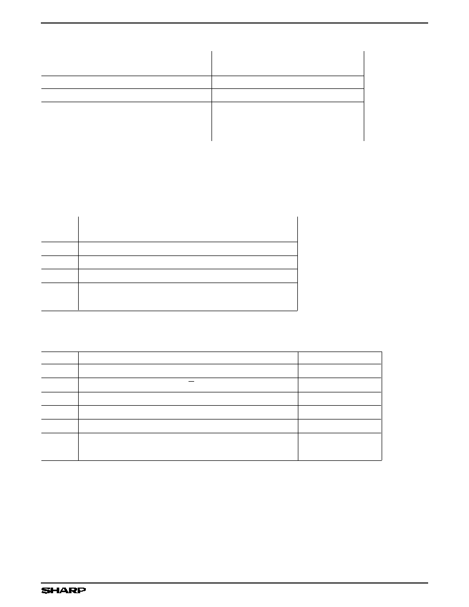
TIMING DIAGRAMS
t
RS
EFL
t
RSR
t
RRSS
t
WRSS
t
FFH
t
HFH
t
,
RS
R,W
EF
FF,HF
5496-14
NOTES:
1. t
RSC
= t
RS
+ t
RSR
.
2. W and R
V
IH
around the rising edge of RS.
3. The Data Out pins (D
0
- D
8
) are forced into a
high-impedance state whenever EF = LOW.
t
RSC
Figure 5. Reset Timing
W
t
WPW
t
RLZ
t
A
t
WC
t
A
t
RPW
t
DV
t
RHZ
VALID DATA OUT
t
RR
R
t
RC
t
WR
t
DH
t
DS
5496-5
Q
0
- Q
8
D
0
- D
8
VALID DATA OUT
VALID DATA IN
VALID DATA IN
Figure 6. Asynchronous Write and Read Operation
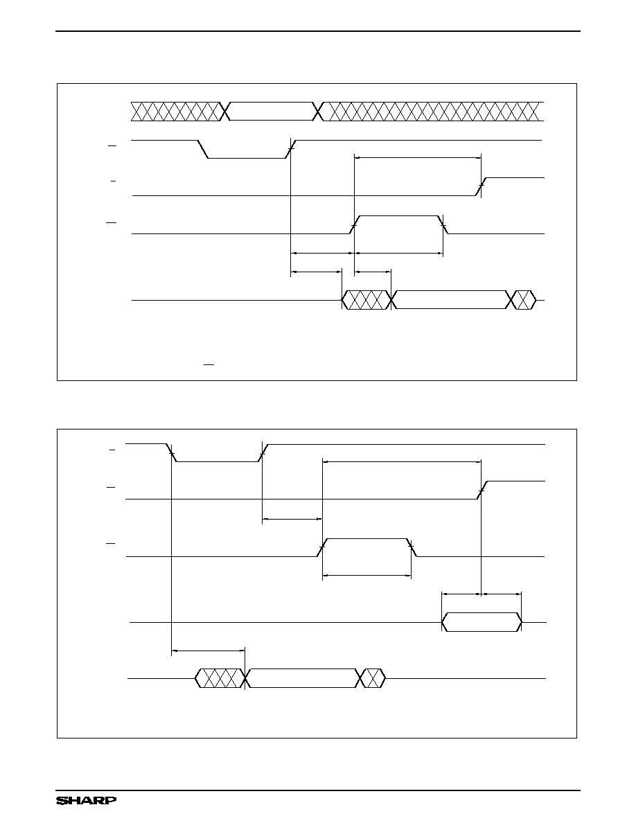
CMOS 512
◊
9 FIFO
LH5496/96H
7

FF
R
t
RFF
t
WFF
LAST WRITE
FIRST READ
W
5496-6
Figure 7. Full Flag from Last Write to First Read
EF
W
R
t
WEF
t
REF
LAST READ
FIRST WRITE
5496-7
NOTE: The Data Out pins (D
0
- D
8
) are forced into a
high-impedance state whenever EF = LOW.
Figure 8. Empty Flag from Last Read to First Write
TIMING DIAGRAMS (cont'd)
LH5496/96H
CMOS 512
◊
9 FIFO
8
TIMING DIAGRAMS (cont'd)
RPE
t
WEF
t
REF
t
WLZ
t
A
t
5496-8
W
R
EF
D
0
- D
8
Q
0
- Q
8
VALID DATA OUT
VALID DATA IN
NOTES:
1. t
RPE
= t
RPW
2. t
RPE
: Effective Read Pulse Width after Empty Flag HIGH.
3. The Data Out pins (D
0
- D
8
) are forced into a
high-impedance state whenever EF = LOW.
Figure 9. Read Data Flow-Through
WPF
t
R
W
FF
t
WFF
t
RFF
t
DH
t
DS
t
A
D
0
- D
8
Q
0
- Q
8
5496-9
NOTES:
1. t
WPF
= t
WPW
2. t
WPF
: Effective Write Pulse Width after Full Flag HIGH.
VALID DATA OUT
VALID DATA IN
Figure 10. Write Data Flow-Through
CMOS 512
◊
9 FIFO
LH5496/96H
9
TIMING DIAGRAMS (cont'd)
t
WEF
W
t
RPE
EF
R
5496-10
NOTES:
1. t
RPE
= t
RPW
2. t
RPE
: Effective Read Pulse Width after Empty Flag HIGH.
3. The Data Out pins (D
0
- D
8
) are forced into a
high-impedance state whenever EF = LOW.
Figure 11. Empty Flag Timing
R
FF
W
5496-11
NOTES:
1. t
WPF
= t
WPW
2. t
WPF
: Effective Write Pulse Width after Full Flag HIGH.
t
RFF
t
WPF
Figure 12. Full Flag Timing
HF
W
R
t
RHF
t
WHF
5496-12
HALF-FULL
OR LESS
MORE THAN
HALF-FULL
HALF-FULL
OR LESS
LH5496/96H
CMOS 512
◊
9 FIFO
10
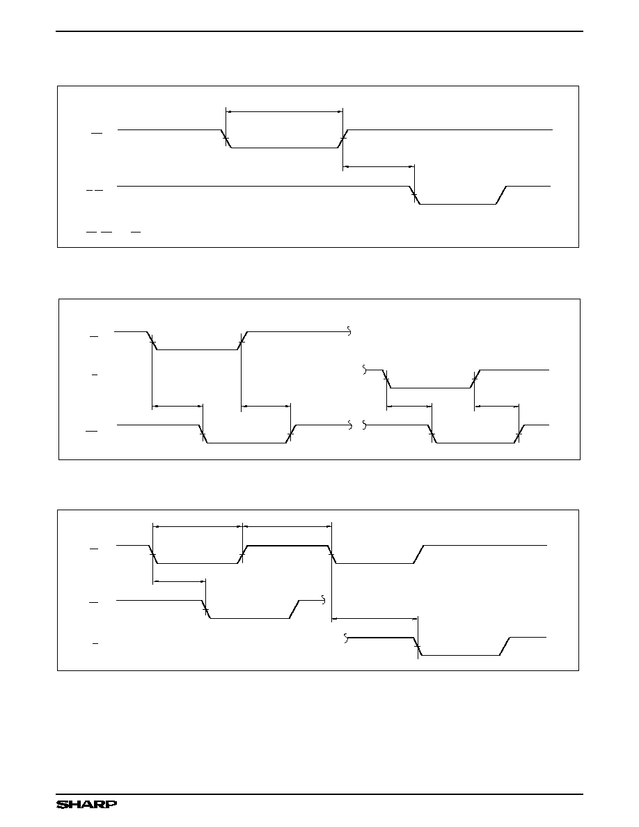
TIMING DIAGRAMS (cont'd)
5496-13
NOTES:
1. t
RTC
= t
RT
+ t
RTR
2. EF, HF and FF may change state during retransmit, but flags will be valid at t
RTC
.
RT
t
RTR
t
RT
R,W
Figure 14. Retransmit Timing
t
XOL
t
XOH
READ FROM
LAST VALID
LOCATION
t
XOH
t
XOL
XO
5496-15
WRITE TO LAST
AVAILABLE
LOCATION
W
R
Figure 15. Expansion Out Timing
t
XIS
R
5496-16
XI
W
WRITE TO FIRST
AVAILABLE
LOCATION
t
XIS
READ FROM FIRST
VALID
LOCATION
t
XIR
t
XI
Figure 16. Expansion In Timing
CMOS 512
◊
9 FIFO
LH5496/96H
11
OPERATIONAL MODES
Single Device Configuration
When depth expansion is not required for the given
application, the device is placed in Single mode by tying
the Expansion In pin (XI) to ground. This pin is internally
sampled during reset.
Width Expansion
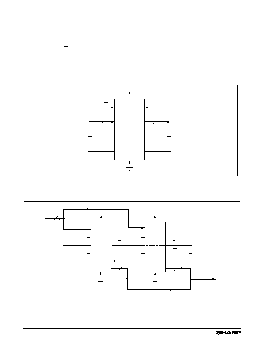
Word-width expansion is implemented by placing mul-
tiple LH5496/96H devices in parallel. Each LH5496/96H
should be configured for standalone mode. In this ar-
rangement, the behavior of the status flags is identical for
all devices; so, in principle, a representative value for
each of these flags could be derived from any one device.
In practice, it is better to derive `composite' flag values
using external logic, since there may be minor speed
variations between different actual devices. (See Figures
17 and 18.)
WRITE
DATA IN
D
0
- D
8
9
FULL FLAG
RESET
XI
RT
RETRANSMIT
EMPTY FLAG
9
READ
HF
LH5496/96H
W
FF
RS
R
EF
DATA OUT
Q
0
- Q
8
5496-17
Figure 17. Single FIFO (512
◊
9)
DATA IN
18
WRITE
FULL FLAG
RESET
9
READ
EMPTY FLAG
R
EF
XI
RT
R
W
5496-18
RS
RETRANSMIT
RT
XI
HF
W
FF
RS
9
18
DATA OUT
9
HF
9
LH5496/96H
LH5496/96H
Figure 18. FIFO Width Expansion (512
◊
18)
LH5496/96H
CMOS 512
◊
9 FIFO
12

OPERATIONAL MODES (cont'd)
Depth Expansion
Depth expansion is implemented by configuring the
required number of FIFOs in Expansion mode. In this
arrangement, the FIFOs are connected in a circular fash-
ion with the Expansion Out pin (XO) of each device tied
to the Expansion In pin (XI) of the next device. One FIFO
in this group must be designated as the first load device.
This is accomplished by tying the First Load pin (FL) of
this device to ground. All other devices must have their
FL pin tied to a high level. In this mode, W and R signals
are shared by all devices, while internal logic controls the
steering of data. Only one FIFO will be enabled for any
given read cycle, so the common Data Out pins of all
devices are wire-ORed together. Likewise, the common
Data In pins of all devices are tied together.
In Expansion mode, external logic is required to gen-
erate a composite Full or Empty flag. This is achieved by
ORing the FF pins of all devices and ORing the EF pins
of all devices respectively. The Half-Full flag and
Retransmit functions are not available in Depth Expan-
sion mode.
5496-19
RS
RS
FF
9
9
RS
W
FF
DATA IN
D
0
- D
8
RS
FF
9
9
9
R
9
DATA OUT
Q
0
- Q
8
FL
FL
EF
XI
XO
FL
EF
Vcc
Vcc
XO
XO
9
9
XI
XI
EMPTY
FULL
EF
LH5496/96H
LH5496/96H
LH5496/96H
Figure 19. FIFO Depth Expansion (1536
◊
9)
CMOS 512
◊
9 FIFO
LH5496/96H
13

OPERATIONAL MODES (cont'd)
Compound Expansion
A combination of width and depth expansion can be
easily implemented by operating groups of depth
expanded FIFOs in parallel.
Bidirectional Operation
Applications which require bidirectional data buffering
between two systems can be realized by operating
LH5496/96H devices in parallel but opposite directions.
The Data In pins of a device may be tied to the corre-
sponding Data Out pins of another device operating in the
opposite direction to form a single bidirectional bus inter-
face. Care must be taken to assure that the appropriate
read, write, and flag signals are routed to each system.
Both depth and width expansion may be used in this
configuration.
LH5496/96H
DEPTH EXPANSION
BLOCK
LH5496/96H
DEPTH EXPANSION
BLOCK
LH5496/96H
DEPTH EXPANSION
BLOCK
Q
0
- Q
8
DATA OUT
D
N-9
- D
N-1
D
18
- D
N-1
D
9
- D
N-1
D
0
- D
N-1
DATA IN
R
W
RS
Q
0
- Q
N-1
Q
0
- Q
17
5496-20
Q
0
- Q
N-10
Figure 20. Compound FIFO Expansion
LH5496/96H
LH5496/96H
SYSTEM A
SYSTEM B
Qb0 - 8
Db0 - 8
Da0 - 8
Qa0 - 8
XI
Wb
Ra
EFa
HFa
RTa
RS
FFb
RTb
HFb
EFb
Rb
5496-21
XI
Wa
FFa
RS
Figure 21. Bidirectional FIFO Buffer
LH5496/96H
CMOS 512
◊
9 FIFO
14

PACKAGE DIAGRAMS
28SK-DIP (DIP028-P-0300)
DIMENSIONS IN MM [INCHES]
MAXIMUM LIMIT
MINIMUM LIMIT
1
14
15
28
28DIP-1
7.05 [0.278]
6.65 [0.262]
0.51 [0.020] MIN.
4.40 [0.173]
4.00 [0.157]
3.40 [0.134]
3.00 [0.118]
2.54 [0.100]
TYP.
0.56 [0.022]
0.36 [0.014]
0.35 [0.014]
0.15 [0.006]
DETAIL
35.00 [1.378]
34.40 [1.354]
0
∞
TO 15
∞
3.65 [0.144]
3.25 [0.128]
7.62 [0.300]
TYP.
28-pin, 300-mil PDIP
DIMENSIONS IN MM [INCHES]
MAXIMUM LIMIT
MINIMUM LIMIT
28DIP (DIP028-P-0600)
1
14
15
28
28DIP-2
13.45 [0.530]
12.95 [0.510]
0.51 [0.020] MIN.
5.20 [0.205]
5.00 [0.197]
3.50 [0.138]
3.00 [0.118]
2.54 [0.100]
TYP.
0.60 [0.024]
0.40 [0.016]
0.30 [0.012]
0.20 [0.008]
DETAIL
36.30 [1.429]
35.70 [1.406]
0
∞
TO 15
∞
4.50 [0.177]
4.00 [0.157]
15.24 [0.600]
TYP.
28-pin, 600-mil PDIP
CMOS 512
◊
9 FIFO
LH5496/96H
15

ORDERING INFORMATION
1.27 [0.050]
4 SIDES BSC
14.05 [0.553]
13.89 [0.547]
15.11 [0.595]
14.86 [0.585]
11.51 [0.453]
11.35 [0.447]
12.57 [0.495]
12.32 [0.485]
3.56 [0.140]
3.12 [0.123]
2.41 [0.095]
1.52 [0.060]
0.81 [0.032]
0.66 [0.026]
0.53 [0.021]
0.33 [0.013]
32PLCC
MAXIMUM LIMIT
MINIMUM LIMIT
DIMENSIONS IN MM (INCHES)
0.38 [0.015]
MIN
DETAIL
10.92 [0.430]
9.91 [0.390]
13.46 [0.530]
12.45 [0.490]
0.10 [0.004]
32PLCC (PLCC32-P-R450)
32-pin, 450-mil PLCC
15
*
20
25
35
50
65
80
Blank 28-pin, 600-mil Plastic DIP (DIP28-P-600)
D 28-pin, 300-mil Plastic DIP (DIP28-P-300)
U 32-pin Plastic Leaded Chip Carrier (PLCC32-P-R450)
LH5496/96H
Device Type
X
Package
- ##
Speed
CMOS 1K x 9 FIFO
Access Time (ns)
X
Temperature
Range
Blank Commercial (0
∞
C to 70
∞
C)
H Industrial (-40
∞
C to 85
∞
C)
5496MD
Example: LH5496U-25 (CMOS 512 x 9 FIFO, 32-pin PLCC, 25 ns)
*
LH5496 only
LH5496/96H
CMOS 512
◊
9 FIFO
16