LH5PV16256
CMOS 4M (256K
◊
16) Pseudo-Static RAM
FEATURES
∑∑
262,144 words
◊
16 bit organization
∑∑
Power supply: +3.0
±
0.15 V
∑∑
Access time: 120 ns (MAX.)
∑∑
Cycle time: 190 ns (MIN.)
∑∑
Power consumption (MAX.):
126 mW (Operating)
94.5
µ
W (Standby = CMOS input level)
220.5
µ
W
(Self-refresh = CMOS input level)
∑∑
LVTTL compatible I/O
∑∑
Available for address refresh,
auto-refresh, and self-refresh modes
∑∑
2,048 refresh cycles/32 ms
∑∑
Address non-multiple
∑∑
Available for byte write mode using UWE
and LWE pins
∑∑
Package:
44-pin, TSOP (Type II)
∑∑
Process: Silicon-gate CMOS
∑∑
Operating temperature: 0 - 70
∞
C
∑∑
Not designed or rated as radiation
hardened
DESCRIPTION
The LH5PV16256 is a 4M bit Pseudo-Static RAM with
a 262,144 words
◊
16 bit organization.
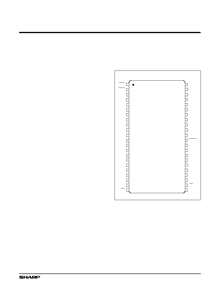
PIN CONNECTIONS
2
3
4
5
6
9
10
7
8
UWE
11
1
44
43
42
41
38
37
40
39
36
35
GND
I/O
15
44-PIN TSOP (Type II)
12
15
13
14
33
32
34
31
30
LWE
A
1
A
0
A
3
A
4
V
CC
V
CC
I/O
6
I/O
13
I/O
14
I/O
11
I/O
12
I/O
10
I/O
9
RFSH
I/O
7
I/O
5
5PV16256S-1
A
5
A
17
CS
A
16
A
15
A
14
A
13
17
18
19
20
21
22
A
11
16
29
28
27
26
23
25
24
I/O
3
A
12
A
9
A
10
CE
I/O
1
I/O
2
OE
I/O
0
GND
A
2
A
6
A
8
A
7
I/O
4
I/O
8
TOP VIEW
Figure 1. Pin Connections
1

PIN DESCRIPTION
PIN NAME
FUNCTION
A
7
- A
17
Row address input
A
0
- A
6
Column address input
UWE, LWE
Upper/lower write enable input
OE
Output enable input
RFSH
Refresh input
CE
Chip enable input
PIN NAME
FUNCTION
CS
Chip select input
I/O
8
- I/O
15
Upper byte data input/output
I/O
0
- I/O
7
Lower byte data input/output
V
CC
Power supply
GND
Ground
I/O
1
CLOCK
GENERATOR
CS
A
5
A
4
A
3
A
10
A
11
A
12
A
13
A
14
A
15
A
16
A
6
A
17
A
9
A
8
A
7
COLUMN
ADDRESS
BUFFER
ROW
ADDRESS
BUFFER
REFRESH
ADDRESS
COUNTER
DATA
IN
BUFFER
DATA
OUT
BUFFER
I/O
SELECTOR
COLUMN
DECODER
SENSE
AMPS
MEMORY
ARRAY 8M
ROW
DECODER
EXT/INT
ADDRESS
MUX.
REFRESH
CONTROLLER
REFRESH
TIMER
I/O
2
I/O
3
I/O
4
I/O
5
I/O
6
I/O
7
V
BB
GENERATOR
GND
V
CC
A
2
A
1
5PV16256S-2
I/O
0
RFSH
OE
21
20
19
18
17
16
15
14
13
12
10
9
8
7
6
5
4
11
33
24
44
35
25
26
27
28
29
30
31
32
CE 22
A
0
3
LWE
UWE 2
1
A
0
-
A
6
A
7
-
A
17
I/O
9
I/O
10
I/O
11
I/O
12
I/O
13
I/O
14
I/O
15
I/O
8
36
37
38
39
40
41
42
43
GND
23
V
CC
34
Figure 2. LH5PV16256 Block Diagram
LH5PV16256
CMOS 4M (256
◊
16) Pseudo-Static RAM
2

TRUTH TABLE
CE
CS
RFSH
OE
UWE
LWE
MODE
I/O
0 - 7
I/O8 - 15
L
H
H
L
H
H
Word Read
Output data
Output data
L
H
H
X
H
L
Write
Lower byte write
Input data
Don't care
L
H
Upper byte write
Don't care
Input data
L
L
Word write
Input data
Input data
H
H
Invalid
High-Z
High-Z
H
X
L
X
X
X
Auto refresh
High-Z
High-Z
L
L
H
X
X
X
CS standby
High-Z
High-Z
H
X
H
X
X
X
Standby
High-Z
High-Z
NOTES:
H = High
L = Low
X = Don't care
REQUIREMENTS
2WE control
Please do not separate the UWE and LWE operation timing intentionally in the same write cycles. Each of the
UWE/LWE should satisfy the timing specifications individually.
Refresh after self-refresh or data retention mode
∑∑
If address refresh is used during normal read/write cycles, the first address refresh must be executed within
15
µ
s after self-refresh or data retention mode ends and the address refresh must be executed continuously for
2,048 refresh cycles.
∑∑
If distributed auto-refresh is used during normal read/write cycles, the first auto-refresh must be executed within
15
µ
s after self-refresh or data retention mode ends.
∑∑
If burst auto-refresh is used during normal read/write cycles, the first auto-refresh must be executed within
15
µ
s after self-refresh or data retention mode ends, and the auto-refresh must be executed continuously for
2,048 refresh cycles.
Bypass capacitor for power supply noise reduction
Because a PSRAM operates dynamically like a DRAM, it is recommended to put bypass capacitors between V
CC
and GND to absorb power supply noise due to the peak current.
CMOS 4M (256
◊
16) Pseudo-Static RAM
LH5PV16256
3

ABSOLUTE MAXIMUM RATINGS
PARAMETER
SYMBOL
RATING
UNIT
NOTE
Supply voltage
V
T
-0.5 to +4.6
V
1
Output short circuit current
I
O
50
mA
Power dissipation
P
D
600
mW
Operating temperature
T
OPR
0 to +70
∞
C
Storage temperature
T
STG
-65 to +150
∞
C
NOTE:
1.
The maximum applicable voltage on any pin with respect to GND.
RECOMMENDED OPERATING CONDITIONS (T
A
= 0 to +70
∞
C)
PARAMETER
SYMBOL
MIN.
TYP.
MAX.
UNIT
NOTE
Supply voltage
V
CC
2.85
3.0
3.15
V
1
GND
0
0
0
V
1
Input voltage
V
IH
2.0
V
CC
+ 0.3
V
V
IL
-0.3
0.8
V
NOTE:
1.
The supply voltage with all V
CC
pins must be on the same level. The supply voltage with all GND pins must be on the same level.
PIN CAPACITANCE (T
A
= 0 to +70
∞
C, f = 1 MHz, V
CC
= 3.0 V
±
0.15 V)
PARAMETER
CONDITIONS
SYMBOL
MIN.
MAX.
UNIT
Input capacitance
A
0
- A
17
C
IN1
8
pF
UWE, LWE
OE, RFSH
C
IN2
8
pF
CE, CS
C
IN3
8
pF
Input/output capacitance
I/O
0
- I/O
15
C
OUT1
10
pF
DC ELECTRICAL CHARACTERISTICS (T
A
= 0 to +70
∞
C, V
CC
= 3.0 V
±
0.15 V)
PARAMETER
SYMBOL
CONDITIONS
MIN.
MAX.
UNIT
NOTE
Operating current in normal operation
I
CC1
tRC = t
RC
(MIN.)
40
mA
1, 2
Standby current
I
CC2
CE, RFSH = V
IH
(MIN.)
1
mA
1
CE, RFSH = V
CC
- 0.2 V
30
mA
1
Self-refresh average current
I
CC3
CE = V
IH
(MIN.)
RFSH = V
IL
(MAX.)
1
mA
1
CE = V
CC
- 0.2 V,
RFSH = 0.2 V
70
mA
1
Input leakage current
I
LI
0 V
V
IN
6.5 V
0 V on all other pins
-10
10
µ
A
Output leakage current
I
LO
0 V
V
OUT
V
CC
+ 0.3 V
Input/output pins in High-Z
state
-10
10
µ
A
Output HIGH voltage
V
OH
I
OUT
= -1 mA
2.4
V
I
OUT
= -100
µ
A
V
CC
- 0.2
V
Output LOW voltage
V
OL
I
OUT
= 1 mA
0.4
V
I
OUT
= 100
µ
A
0.2
V
Data retention voltage
V
R
2.2
3.15
V
NOTES:
1.
The input/output pins are in high impedance state.
2.
I
CC1
depends on the cycle time.
LH5PV16256
CMOS 4M (256
◊
16) Pseudo-Static RAM
4

AC ELECTRICAL CHARACTERISTICS
1,2,7
(T
A
= 0 to +70
∞
C, V
CC
= 3.0 V
±
0.15 V)
PARAMETER
SYMBOL
MIN.
MAX.
UNIT
NOTES
Random read, write cycle time
t
RC
190
ns
Random modify write cycle time
t
RMW
250
ns
CE pulse width
t
CE
120
10,000
ns
CE precharge time
t
P
60
ns
Address setup time
t
AS
0
ns
3
Row address hold time from CE
t
RAH
30
ns
3
Column address hold time from CE
t
CAH
120
ns
CS setup time from CE
t
CSS
0
ns
CS hold time from CE
t
CSH
30
ns
Read command setup time
t
RCS
0
ns
11
Read command hold time
t
RCH
0
ns
9
CE access time
t
CEA
120
ns
4
OE access time
t
OEA
60
ns
4
CE to output in Low-Z
t
CLZ
20
ns
OE to output in Low-Z
t
OLZ
0
ns
Write disable to output in Low-Z
t
WLZ
0
ns
11
Chip disable to output in High-Z
t
CHZ
0
30
ns
Output disable to output in High-Z
t
OHZ
0
30
ns
WE to output in High-Z
t
WHZ
0
30
ns
9, 13
Write command pulse width
t
WCP
35
ns
13
Write command setup time
t
WCS
35
10,000
ns
10, 13
Write command hold time
t
WCH
120
10,000
ns
12, 13
Data setup time from write disable
t
DSW
30
ns
5, 12, 13
Data setup time from chip disable
t
DSC
30
ns
5
Data hold time from write disable
t
DHW
0
ns
5, 11, 13
Data hold time from chip disable
t
DHC
30
ns
5
Data hold time from column address
t
OH
0
ns
Column address hold time from chip disable
t
AHC
20
ns
5
Column address hold time from write disable
t
AHW
0
ns
5, 13
Transition time (rise and fall)
t
T
3
50
ns
Output disable setup time
t
ODS
0
ns
Output disable hold time
t
ODH
15
ns
Refresh time interval (2048 cycle)
t
REF
32
ms
6
Auto refresh cycle time
t
FC
190
ns
6
Refresh delay time from CE
t
RFD
90
ns
Refresh pulse width (Auto refresh)
t
FAP
80
1,000
ns
8
Refresh precharge time (Auto refresh)
t
FP
40
ns
CE delay time from refresh enable
(Auto refresh)
t
FCE
190
ns
Refresh pulse width (Self refresh)
t
FAS
8,000
ns
8
CE delay time from refresh precharge
(Self refresh)
t
FRS
600
ns
V
CC
recovery time from data retention
t
R
5
ms
Refresh setup hold time
t
FS
0
ns
Refresh disable hold time
t
RDH
15
ns
Chip disable delay time from RFSH
t
RDD
15
ns
CMOS 4M (256
◊
16) Pseudo-Static RAM
LH5PV16256
5